

For free samples & the latest literature: http://www.maxim-ic.com, or phone 1-800-998-8800.
For small orders, phone 1-800-835-8769.
General Description
The MAX4588 low-voltage, dual 4-channel multiplexer
is designed for RF and video signal processing at frequencies up to 180MHz in 50Ω and 75Ω systems. A
flexible digital interface allows control of on-chip functions through either a parallel interface or an SPI™/
MICROWIRE™ serial port.
Each channel of the MAX4588 is designed using a “T”
switch configuration, ensuring excellent high-frequency
off-isolation. The MAX4588 has low on-resistance of
60Ω max, with an on-resistance match across all chan-
nels of 4Ω max. Additionally, on-resistance is flat
across the specified signal range (2Ω max). The offleakage current is under 1nA at TA= +25°C, and less
than 10nA at TA= +85°C.
The MAX4588 operates from single +2.7V to +12V or
dual ±2.7V to ±6V supplies. When operating with a +5V
supply, the inputs maintain TTL- and CMOS-level compatibility. The MAX4588 is available in 28-pin narrow
DIP, wide SO, and space-saving SSOP packages.
Applications
RF Switching Automatic Test Equipment
Video Signal Routing Networking
High-Speed Data Acquisition
Features
♦ Low Insertion Loss: -2.5dB up to 100MHz
♦ High Off-Isolation: -74dB at 10MHz
♦ Low Crosstalk: -70dB up to 10MHz
♦ 16MHz -0.1dB Signal Bandwidth
♦ 180MHz -3dB Signal Bandwidth
♦ 60Ω (max) On-Resistance with ±5V Supplies
♦ 4Ω (max) On-Resistance Matching with ±5V
Supplies
♦ 2Ω (max) On-Resistance Flatness with ±5V
Supplies
♦ +2.7V to +12V Single Supply
±2.7V to ±6V Dual Supplies
♦ Low Power Consumption: <20µW
♦ Rail-to-Rail
®
, Bidirectional Signal Handling
♦ Parallel or SPI/MICROWIRE-Compatible Serial
Interface
♦ >±2kV ESD Protection per Method 3015.7
♦ TTL/CMOS-Compatible Inputs with V
L
= +5V
MAX4588
Low-Voltage, High-Isolation,
Dual 4-Channel RF/Video Multiplexer
________________________________________________________________
Maxim Integrated Products
1
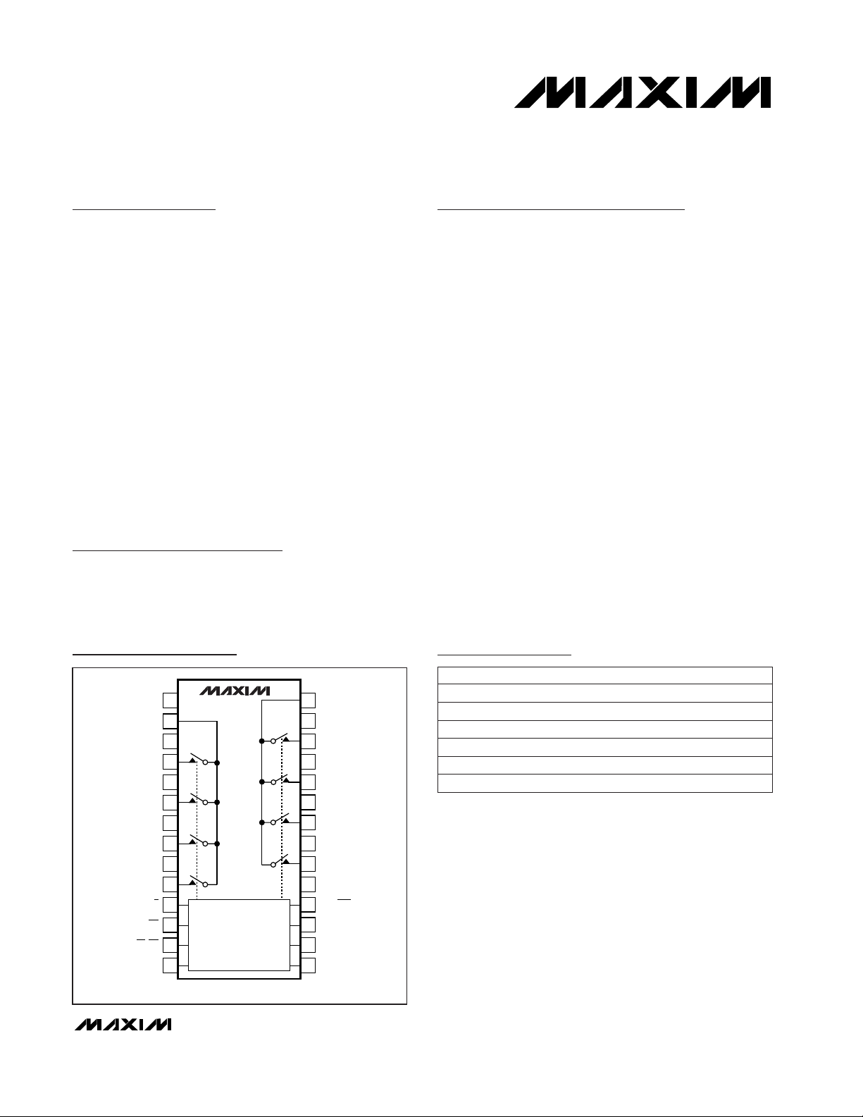
28
27
26
25
24
23
22
21
20
19
18
17
16
15
1
2
3
4
5
6
7
8
9
10
11
12
13
14
COM2
VNO5
GND
NO6
GND
A1/DIN
NO7
GND
NO8
V
L
SER/PAR
EN
A0/DOUT
A2/SCLK
LE/CS
RS
4/8
NO4
GND
NO3
GND
NO2
GND
NO1
V+
COM1
GND
SSOP/SO/DIP
TOP VIEW
MAX4588
CONTROL
LOGIC
19-1425; Rev 0; 1/99
PART TEMP. RANGE PIN-PACKAGE
Pin Configuration
Ordering Information
MAX4588CPI 0°C to +70°C 28 Narrow Plastic DIP
MAX4588EAI
MAX4588EWI -40°C to +85°C
-40°C to +85°C 28 SSOP
28 Wide SO
MAX4588EPI -40°C to +85°C 28 Narrow Plastic DIP
SPI is a trademark of Motorola, Inc.
MICROWIRE is a trademark of National Semiconductor Corp.
Rail-to-Rail is a registered trademark of Nippon Motorola, Ltd.
MAX4588CAI
0°C to +70°C 28 SSOP
MAX4588CWI 0°C to +70°C 28 Wide SO
MAX4588
Low-Voltage, High-Isolation,
Dual 4-Channel RF/Video Multiplexer
2 _______________________________________________________________________________________
ABSOLUTE MAXIMUM RATINGS
ELECTRICAL CHARACTERISTICS—Dual Supplies
(V+ = VL= +4.5V to +5.5V, V- = -4.5V to -5.5V, V
INH
= +2.4V, V
INL
= +0.8V, TA= T
MIN
to T
MAX
, unless otherwise noted. Typical val-
ues are at T
A
= +25°C, V+ = VL= +5V, V- = -5V.) (Note 2)
Stresses beyond those listed under “Absolute Maximum Ratings” may cause permanent damage to the device. These are stress ratings only, and functional
operation of the device at these or any other conditions beyond those indicated in the operational sections of the specifications is not implied. Exposure to
absolute maximum rating conditions for extended periods may affect device reliability.
(Voltages referenced to GND)
V+........................................................................-0.3V to +13.0V
V
L
.......................-0.3V to (V+ + 0.3V) or 7V (whichever is lower)
V- ........................................................................-13.0V to +0.3V
V+ to V-................................................................-0.3V to +13.0V
V
NO_
, V
COM_
(Note 1) ..........................(V- - 0.3V) to (V+ + 0.3V)
4/
8, RS, LE/CS, A2/SCLK, A1/DIN,
A0/DOUT, EN, SER/PAR to GND...............-0.3V to (V+ + 0.3V)
Continuous Current into Any Terminal..............................±20mA
Peak Current into Any Terminal
(pulsed at 1ms, 10% duty cycle)..................................±40mA
ESD per Method 3015.7.......................................................±2kV
Continuous Power Dissipation (T
A
= +70°C)
SSOP (derate 9.52mW/°C above +70°C) ....................762mW
Wide SO (derate 12.50mW/°C above +70°C)................1.00W
Plastic DIP (derate 14.29mW/°C above +70°C) ............1.14W
Operating Temperature Ranges
MAX4588C_ I......................................................0°C to +70°C
MAX4588E_ I ...................................................-40°C to +85°C
Storage Temperature Range.............................-65°C to +150°C
Lead Temperature (soldering, 10sec).............................+300°C
Note 1: Voltages on these pins exceeding V+ or V- are clamped by internal diodes. Limit forward diode current to maximum current
rating.
+25°C
V+ = 5V, V- = -5V, V
NO_
= ±2V,
I
COM_
= 4mA
C, E
+25°C
C, E
C, E
+25°C
C, E
+25°C
T
A
+25°C
V+ = 5.5V, V- = -5.5V,
V
COM_
= ±4.5V, V
NO_
=
–
+
4.5V
V+ = 5V, V- = 5V, V
NO_
= ±2V,
I
COM_
= 4mA
C, E
V+ = 5V; V- = -5V; V
NO_
= 1V, 0, -1V;
I
COM_
= 1mA
+25°C
CONDITIONS
V+ = 5.5V, V- = -5.5V, V
COM_
= ±4.5V,
V
NO_
= ±4.5V or floating
C, E
V+ = 5.5V, V- = -5.5V,
V
COM_
= ±4.5V, V
NO_
=
–
+
4.5V
C, E
C, E
C, E
V
IN_
= 0 or V
L
nA
-2 0.01 2
I
COM_(ON)
COM_ On-Leakage Current
(Note 6)
-20 20
nA
-2 0.01 2
I
COM_(OFF)
COM_ Off-Leakage Current
(Note 6)
LOGIC OUTPUT (SERIAL
µA-1 0.03 1I
IN
Input Current
V0.2Input Threshold Hysteresis
-20 20
LOGIC INPUTS (Pins 11
V2.4 1.7V
INH
Ω
40 60
R
ON
On-Resistance
VV- V+
V
COM_
,
V
NO
ANALOG SWITCH
Analog Signal Range
(Note 3)
Input Logic Threshold High
V1.5 0.8V
INL
-10 10
nA
-1 0.01 1
I
NO_(OFF)
NO_ Off-Leakage Current
(Note 6)
Ω
3
75
Ω
14
∆R
ON
On-Resistance Match Between
Channels (Note 4)
5
0.5 2.5
R
FLAT(ON)
On-Resistance Flatness
(Note 5)
UNITSMIN TYP MAXSYMBOLPARAMETER
Input Logic Threshold Low
C, E
C, E
I
SOURCE
= -1mA
I
SINK
= 3.2mA
VVL - 1V
OH
V0.4V
OL
DOUT Logic Low Output
DOUT Logic High Output
ANALOG SWITCH
LOGIC INPUTS (4/8, RS, LE/CS, A2/SCLK, A1/DIN, A0/DOUT, EN, SER/PAR)
LOGIC OUTPUT (SERIAL INTERFACE)
MAX4588
Low-Voltage, High-Isolation,
Dual 4-Channel RF/Video Multiplexer
_______________________________________________________________________________________ 3
ELECTRICAL CHARACTERISTICS—Dual Supplies (continued)
(V+ = VL= +4.5V to +5.5V, V- = -4.5V to -5.5V, V
INH
= +2.4V, V
INL
= +0.8V, TA= T
MIN
to T
MAX
, unless otherwise noted. Typical val-
ues are at T
A
= +25°C, V+ = VL= +5V, V- = -5V.) (Note 2)
4-channel mode
T
A
8-channel mode
4-channel mode
8-channel mode
CONDITIONS UNITSMIN TYP MAXSYMBOLPARAMETER
+25°C
+25°C
C, E
+25°C
C, E
+25°C
C, E
V
NO_
= 0, fIN= 1MHz, Figure 4
+25°C
CL= 1.0nF, V
NO_
= 0, RS= 0,
Figure 3
V
NO_
= ±3V, V+ = 5.5V, V- = -5.5V,
Figure 2
V
NO_
= 3V, V+ = 4.5V, V- = -4.5V,
Figure 1
V
NO_
= 3V, V+ = 4.5V, V- = -4.5V,
Figure 1
+25°C
+25°C
V
NO_
= 1V
RMS
, f = 10MHz,
all channels off, Figure 5
V
COM_
= 0, fIN= 1MHz, Figure 4
+25°C
V
COM_
= 0, fIN= 1MHz, Figure 4
+25°C
+25°C
Figure 5
V
NO_
= 1V
RMS
, f = 10MHz, Figure 5
Figure 5
V
ISO
Off-Isolation (Note 7)
pF7C
COM_(ON)
pF4
C
COM_(OFF)
COM_ Off-Capacitance
COM_ On-Capacitance
PARALLEL MODE INPUT TIM-
11
MHz
16
BW-0.1dB Bandwidth
dB-74
dB-70V
CT
Channel-to-Channel Crosstalk
MHz
180
BW
SWITCH DYNAMIC CHARAC-
-3dB Bandwidth
140
pF2C
NO_(OFF)
NO_ Off-Capacitance
pC15QCharge Injection
ns10 180t
BBM
Break-Before-Make Time Delay
(Note 3)
ns
380 550
t
ON
Turn-On Time
600
ns
150 300
t
OFF
Turn-Off Time
350
C, EFigure 6
C, E
C, E
C, E
C, E
C, E
C, E
Figure 7
C, E
Figure 7
Figure 7
Figure 6
Figure 6
Figure 6
C, E
C, E
Figure 7
Figure 7
Figure 7
C, E
C, E
C, E
Figure 7
Figure 7
Figure 7
ns50t
CSS0
CS Fall to SCLK Rise Setup Time
ns0t
DH
ns60t
DS
DIN to SCLK Rise Setup Time
DIN to SCLK Rise Hold Time
ns0t
CSH1
CS
Rise to SCLK Rise Hold Time
ns80t
CSS1
CS
Rise to SCLK Rise Setup
Time
ns80t
CSS1
ns80t
DS
A_, EN to LE Rise Setup Time
CS
Fall to SCLK Rise Hold Time
ns80t
CL
SCLK Pulse Width Low
ns80t
CH
SCLK Pulse Width High
MHz6.25f
CLK
Operating Frequency
ns0t
DH
A_, EN to LE Rise Hold Time
ns80t
L
LE Low Pulse Width
ns80t
RS
RS Low Pulse Width
SERIAL PERIPHERAL INTER-
C, EFigure 6 ns80t
RS
RS Low Pulse Width
C, ECL= 50pF, Figure 7 ns150t
DO
SCLK Rise to DOUT Valid
SERIAL-INTERFACE TIMING
PARALLEL-INTERFACE TIMING
SWITCH DYNAMIC CHARACTERISTICS
V+ = 5.5V
MAX4588
Low-Voltage, High-Isolation,
Dual 4-Channel RF/Video Multiplexer
4 _______________________________________________________________________________________
ELECTRICAL CHARACTERISTICS—Dual Supplies (continued)
(V+ = VL= +4.5V to +5.5V, V- = -4.5V to -5.5V, V
INH
= +2.4V, V
INL
= +0.8V, TA= T
MIN
to T
MAX
, unless otherwise noted. Typical val-
ues are at T
A
= +25°C, V+ = VL= +5V, V- = -5V.) (Note 2)
T
A
CONDITIONS UNITSMIN TYP MAXSYMBOLPARAMETER
2.7 V+V
L
V
±2.7 ±6V+, V-
Power-Supply Range
POWER SUPPLY
+25°C
C, E
+25°C
V+ = 5.5V, V- = -5.5V
V+ = 5.5V, V- = -5.5V
C, E
C, EVL= 5.5V, all V
IN_
= 0 or V
L
µA
-1 0.0001 1
I-V - Supply Current
-10 10
µA
-1 0.0001 1
I+V+ Supply Current
-10 10
µA-10 2 10I
L
VLSupply Current
ELECTRICAL CHARACTERISTICS—Single +5V Supply
(V+ = VL= +4.5V to +5.5V, V- = 0, V
INH
= +2.4V, V
INL
= +0.8V, TA= T
MIN
to T
MAX
, unless otherwise noted. Typical values are at T
A
= +25°C, V+ = VL= +5V.) (Note 2)
+25°C
V+ = 5V, V
NO_
= 3V, I
COM_
= 4mA
C, E
+25°C
C, E
C, E
+25°C
C, E
+25°C
T
A
+25°C
V+ = 5.5V; V
COM_
= 4.5V, 1V;
V
NO_
= 1V, 4.5V
V
NO_
= 2V, 3V, 4V
V+ = 5V, V
NO_
= 3V, I
COM_
= 4mA
C, E
V+ = 5V, I
COM_
= 4mA,
+25°C
CONDITIONS
V+ = 5.5V; V
COM_
= 4.5V, 1V;
V
NO_
= 4.5V, 1V, or floating
C, E
V+ = 5.5V; V
COM_
= 4.5V, 1V;
V
NO_
= 1V, 4.5V
C, E
C, E
C, E
VIN= 0 or V
L
nA
-2 0.005 2
I
COM_(ON)
COM_ On Leakage Current
(Notes 6, 9)
-20 20
nA
-2 0.005 2
I
COM(OFF)
COM_ Off Leakage Current
(Notes 6, 9)
LOGIC OUTPUT (SERIAL
µA-1 1I
IN
Input Current
V0.2Input Threshold Hysteresis
-20 20
LOGIC INPUTS (Pins 11 through
V2.4 1.7V
INH
Ω
80 120
R
ON
On-Resistance
V0V+
V
COM_
,
V
NO_
ANALOG SWITCH
Analog Signal Range (Note 3)
Input Logic Threshold High
V1.5 0.8V
INL
-10 10
nA
-1 0.005 1
I
NO_(OFF)
NO_ Off Leakage Current
(Notes 6, 9)
12
150
Ω
18
∆R
ON
On-Resistance Match Between
Channels (Note 4)
10
Ω
410
R
FLAT(ON)
On-Resistance Flatness
(Note 5)
UNITSMIN TYP MAXSYMBOLPARAMETER
Input Logic Threshold Low
C, E
C, E
I
SOURCE
= -1mA
I
SINK
= 3.2mA
VVL- 1V
OH
V0.4V
OL
DOUT Logic Low Output
DOUT Logic High Output
POWER SUPPLY
ANALOG SWITCH
LOGIC INPUTS (4/8, RS, LE/CS, A2/SCLK, A1/DIN, A0/DOUT, EN, SER/PAR)
LOGIC OUTPUT (SERIAL INTERFACE)
V+ = 5V, I
COM_
= 4mA,
V
NO_
= 2V, 3V, 4V
MAX4588
Low-Voltage, High-Isolation,
Dual 4-Channel RF/Video Multiplexer
_______________________________________________________________________________________ 5
ELECTRICAL CHARACTERISTICS—Single +5V Supply (continued)
(V+ = VL= +4.5V to +5.5V, V- = 0, V
INH
= +2.4V, V
INL
= +0.8V, TA= T
MIN
to T
MAX
, unless otherwise noted. Typical values are at T
A
= +25°C, V+ = VL= +5V.) (Note 2)
T
A
CONDITIONS
4-channel mode
8-channel mode
4-channel mode
8-channel mode
UNITSMIN TYP MAXSYMBOLPARAMETER
+25°C
+25°C
C, E
+25°C
C, E
+25°C
C, E
V
NO_
= 1V
RMS
, f = 10MHz,
all channels off, Figure 5
CL= 1.0nF, V
NO_
= 2.5V, RS= 0,
Figure 3
V
NO_
= 3V, V+ = 5.5V, Figure 2
V
NO_
= 3V, V+ = 4.5V, Figure 1
V
NO_
= 3V, V+ = 4.5V, Figure 1
+25°C
+25°C
C, E
C, E
Figure 5
C, E
V
NO_
= 1V
RMS
, f = 10MHz, Figure 5
+25°C
C, E
Figure 6
Figure 6
Figure 6
Figure 5
Figure 6
75
MHz
100
BW
dB-70V
CT
Channel-to-Channel Crosstalk
-3dB Bandwidth
ns80t
RS
RS Low Pulse Width
ns80t
L
LE Low Pulse Width
ns0t
DH
A_, EN to LE Rise Hold Time
MHz
10
BW-0.1dB Bandwidth
7
SWITCH DYNAMIC CHARAC-
PARALLEL MODE INPUT TIM-
ns80t
DS
dB-65V
ISO
Off-Isolation
pC5QCharge Injection
ns10 200t
BBM
Break-Before-Make Time Delay
(Note 3)
ns
550 800
t
ON
Turn-On Time
900
ns
150 300
t
OFF
Turn-Off Time
350
A_, EN to LE Rise Setup Time
C, E
C, E
C, E
C, E
C, E
C, E
C, E
Figure 7
C, E
Figure 7
Figure 7
Figure 7
Figure 7
Figure 7
Figure 7
C, E
CL= 50pF, Figure 7
Figure 7
ns150t
DO
SCLK Rise to DOUT Valid
ns80t
CSS1
CS
Rise to SCLK Rise Setup
Time
SERIAL PERIPHERAL INTER-
ns0t
CSH1
CS
Rise to SCLK Rise Hold Time
ns50t
CSS0
CS Fall to SCLK Rise Setup Time
ns0t
DH
DIN to SCLK Rise Hold Time
MHz6.25f
CLK
Operating Frequency
ns80t
CH
SCLK Pulse Width High
ns80t
CL
SCLK Pulse Width Low
ns60t
DS
DIN to SCLK Rise Setup Time
C, EFigure 6 ns80t
RS
RS Low Pulse Width
C, EFigure 7 ns80t
CSS1
CS
Fall to SCLK Rise Hold Time
SWITCH DYNAMIC CHARACTERISTICS
PARALLEL-INTERFACE TIMING
SERIAL-INTERFACE TIMING
MAX4588
Low-Voltage, High-Isolation,
Dual 4-Channel RF/Video Multiplexer
6 _______________________________________________________________________________________
ELECTRICAL CHARACTERISTICS—Single +5V Supply (continued)
(V+ = VL= +4.5V to +5.5V, V- = 0, V
INH
= +2.4V, V
INL
= +0.8V, TA= T
MIN
to T
MAX
, unless otherwise noted. Typical values are at T
A
= +25°C, V+ = VL= +5V.) (Note 2)
T
A
CONDITIONS UNITSMIN TYP MAXSYMBOLPARAMETER
C, E
C, E
+25°C
VL= 5.5V, all V
IN_
= 0 or V
L
V+ = 5.5V, VIN= 0 or V
L
V+ ≤ 6.5V
V+ > 6.5V
µA-10 2 10I
L
VLSupply Current
-10 10
µA
-1 1
I+V+ Supply Current
POWER SUPPLY
V
2.7 12V+
Power-Supply Range 2.7 V+
V
L
2.7 6.5
ELECTRICAL CHARACTERISTICS—Single +3V Supply
(V+ = VL= +2.7V to +3.6V, V- = 0, V
INH
= +2V, V
INL
= +0.5V, TA= T
MIN
to T
MAX
, unless otherwise noted. Typical values are at TA=
+25°C, V+ = V
L
= +3.0V.)
+25°C
V+ = 2.7V, V
NO_
= 1V,
I
COM_
= 1mA
+25°C
C, E
C, E
C, E
C, E
V
NO_
= 1.5V, V+ = 2.7V, Figure 1
T
A
C, E
V
IN_
= 0 or V
L
+25°C
C, E
CONDITIONS
C, E
V
NO_
= 1.5V, V+ = 2.7V, Figure 1
C, E
+25°C
C, E
Figure 6
Figure 6
V
NO_
= 1.5V, V+ = 3.6V, Figure 2
Figure 6
500
ns
250 400
t
OFF
200
Turn-Off Time
SERIAL PERIPHERAL INTER-
ns200t
L
LE Low Pulse Width
ns0t
DH
A_, EN to LE Rise Hold Time
Break-Before-Make Time Delay
(Note 3)
ns10 350t
BBM
Ω
240 350
R
ON
On-Resistance
V0V+
V
COM_
,
V
NO_
ANALOG SWITCH
Analog Signal Range
PARALLEL MODE INPUT TIM-
ns200t
DS
ns
700 1000
t
ON
Turn-On Time
SWITCH DYNAMIC CHARAC-
µA-1 1I
IN
Input Current
450
LOGIC INPUT (Pins 11 through
V2.0V
INH
Input Logic Threshold High
V0.5V
INL
Input Logic Threshold Low
UNITSMIN TYP MAXSYMBOLPARAMETER
A_, EN to LE Rise Setup Time
C, E
C, E
C, E
Figure 7
Figure 7
Figure 7
C, E
C, E
Figure 7
Figure 7
ns200t
CL
SCLK Pulse Width Low
ns200t
CH
MHz2.1f
CLK
Operating Frequency
SCLK Pulse Width High
ns100t
DS
DIN to SCLK Rise Setup Time
ns0t
DH
DIN to SCLK Rise Hold Time
POWER SUPPLY
C, EFigure 6 ns200t
RS
RS Low Pulse Width
C, EFigure 6 ns200t
RS
RS Low Pulse Width
ANALOG SWITCH
LOGIC INPUTS (4/8, RS, LE/CS, A2/SCLK, A1/DIN, A0/DOUT, EN, SER/PAR)
SWITCH DYNAMIC CHARACTERISTICS
PARALLEL-INTERFACE TIMING
SERIAL-INTERFACE TIMING

MAX4588
Low-Voltage, High-Isolation,
Dual 4-Channel RF/Video Multiplexer
_______________________________________________________________________________________ 7
ELECTRICAL CHARACTERISTICS—Single +3V Supply (continued)
(V+ = VL= +2.7V to +3.6V, V- = 0, V
INH
= +2V, V
INL
= +0.5V, TA= T
MIN
to T
MAX
, unless otherwise noted. Typical values are at TA=
+25°C, V+ = V
L
= +3.0V.)
T
A
CONDITIONS UNITSMIN TYP MAXSYMBOLPARAMETER
C, E
C, E
C, E
C, E
C, E
CL= 50pF, Figure 7
C, E
Figure 7
Figure 7
Figure 7
+25°C
Figure 7
V+ = 3.6V, VIN= 0 or V
L
C, EVL= 3.6V, all VIN= 0 or V
L
-10 10
µA
-1 1
I+
POWER SUPPLY
V+ Supply Current
µA-10 1 10I
L
VLSupply Current
ns250t
DO
SCLK Rise to DOUT Valid
ns200t
CSS1
CS
Fall to SCLK Rise Hold Time
ns200t
CSS1
CS
Rise to SCLK Rise Setup
Time
ns100t
CSS0
CS Fall to SCLK Rise Setup Time
ns0t
CSH1
CS
Rise to SCLK Rise Hold Time
Note 2: The algebraic convention is used in this data sheet; the most negative value is shown in the minimum column.
Note 3: Guaranteed by design.
Note 4: ∆R
ON
= ∆R
ON(MAX)
- ∆R
ON(MIN)
.
Note 5: Resistance flatness is defined as the difference between the maximum and the minimum value of on-resistance as
measured over the specified analog-signal range.
Note 6: Leakage parameters are 100% tested at maximum rated hot temperature and guaranteed by correlation at T
A
= +25°C.
Note 7: Off isolation = 20log
10[VCOM_
/ (V
NC_
or V
NO_
)], V
COM_
= output, V
NC_
or V
NO_
= input to off switch.
Note 8: Between any two switches.
Note 9: Leakage testing for single-supply operation is guaranteed by testing with dual supplies.
POWER SUPPLY
MAX4588
Low-Voltage, High-Isolation,
Dual 4-Channel RF/Video Multiplexer
8 _______________________________________________________________________________________
Typical Operating Characteristics
(V+ = VL= +5V, V- = -5V, TA= +25°C, unless otherwise noted.)
0
30
20
10
40
50
60
70
80
90
100
-6 -2-4 0246
ON-RESISTANCE vs. V
COM
(DUAL SUPPLIES)
MAX4588-01
V
COM
(V)
ON-RESISTANCE (Ω)
±2.5V
±3V
±4V
±5V
±6V
0
50
150
100
200
250
0624
810
12
ON-RESISTANCE vs. V
COM
(SINGLE SUPPLY)
MAX4588-02
V
COM
(V)
ON-RESISTANCE (Ω)
V+ = +2.5V
V- = 0
V+ = +3.6V
V+ = +3.0V
V+ = +5V
V+ = +9V
V+ = +12V
20
30
25
40
35
50
45
55
65
60
70
-5 -3 -2 -1-4 012 435
ON-RESISTANCE vs. V
COM
AND TEMPERATURE (DUAL SUPPLIES)
MAX4588-03
V
COM
(V)
ON-RESISTANCE (Ω)
TA = +85°C
TA = +50°C
TA = +25°C
TA = 0°C
TA = -40°C
40
60
50
80
70
100
90
110
130
120
140
0 1.0 1.5 2.00.5 2.5 3.0 3.5 4.54.0 5.0
ON-RESISTANCE vs. V
COM
AND TEMPERATURE (SINGLE SUPPLY)
MAX4588-04
V
COM
(V)
ON-RESISTANCE (Ω)
TA = +85°C
V- = 0
TA = +50°C
TA = +25°C
TA = 0°C
TA = -40°C
0.1p
1p
10p
100p
1n
10n
-40 40020-20 60 80 100 120
ON/OFF-LEAKAGE CURRENT
vs. TEMPERATURE
MAX4588-05
TEMPERATURE (°C)
LEAKAGE CURRENT (A)
ON-LEAKAGE
OFF-LEAKAGE
0
10
5
20
15
30
25
35
-5 -1-3 1 3-4 0-2 2 4 5
CHARGE INJECTION vs. V
COM
MAX4588-06
V
COM
(V)
CHARGE INJECTION (pC)
DUAL SUPPLIES
SINGLE SUPPLY

MAX4588
Low-Voltage, High-Isolation,
Dual 4-Channel RF/Video Multiplexer
_______________________________________________________________________________________
9
1p
100p
10p
10n
1n
1µ
100n
10µ
-40 0 20-20 40 60 80 100 120
SUPPLY CURRENT vs. TEMPERATURE
MAX4588-09
TEMPERATURE (°C)
SUPPLY CURRENT (A)
I
L
I+
I-
-90
-60
-70
-80
-50
-40
-30
-20
-10
0
10
100k 1M 10M 100M 1G
INSERTION LOSS, OFF-ISOLATION,
AND CROSSTALK vs. FREQUENCY
(DUAL SUPPLIES)
MAX4588-10
FREQUENCY (Hz)
AMPLITUDE (dB)
ON LOSS
RS = 75Ω
R
L
= 600Ω
CROSSTALK
OFF-ISOLATION
-90
-60
-70
-80
-50
-40
-30
-20
-10
0
10
100k 1M 10M 100M 1G
INSERTION LOSS, OFF-ISOLATION,
AND CROSSTALK vs. FREQUENCY
(SINGLE SUPPLY)
MAX4588-11
FREQUENCY (Hz)
AMPLITUDE (dB)
INSERTION LOSS
OFF-ISOLATION
CROSSTALK
RS = 75Ω
R
L
= 600Ω
Typical Operating Characteristics (continued)
(V+ = VL= +5V, V- = -5V, TA= +25°C, unless otherwise noted.)
0
200
100
400
300
500
600
2.5 4.0 4.53.0 3.5 5.0 5.5 6.0
ON/OFF TIME vs. SUPPLY VOLTAGE
MAX4588-07
SUPPLY VOLTAGE (±V)
t
ON,
t
OFF
(ns)
t
OFF
t
ON
0
100
300
200
400
500
-40-30-20-100 1020304050607080
ON/OFF TIME vs. TEMPERATURE
MAX4588-08
TEMPERATURE (°C)
t
ON,
t
OFF
(ns)
t
OFF
t
ON
MAX4588
Low-Voltage, High-Isolation,
Dual 4-Channel RF/Video Multiplexer
10 ______________________________________________________________________________________
Pin Description
Active-Low Reset Input. In serial mode, drive RS low to force the latches and shift registers to the poweron reset state and force all switches open. In parallel mode, drive RS low to force the latches to the poweron reset state and force all switches open. See
Truth Tables
.
RS
12
In parallel mode, this pin is the transparent Latch Enable. In the serial mode, this pin is the Chip-Select
Input. See
Truth Tables.
LE/CS
13
Most Significant Address Bit in parallel mode with 4/8 low. If 4/8 pin is high, this pin is ignored. In the serial
mode, this is the Serial Shift Clock Input. Data is loaded on the rising edge of SCLK. See
Truth Tables
.
A2/SCLK14
Address Input in the parallel mode. Serial Data Input in serial mode. In serial mode, data is loaded on
SCLK’s rising edge.
A1/DIN15
Least Significant Address Input in the parallel mode. In the serial mode this is an output from the internal
4-bit shift register. DOUT is intended for daisy-chain cascading. DOUT is not three-stated by CS. See
Serial Operation
.
A0/DOUT16
Normally Open Analog Input Terminal. See
Truth Tables.
NO26
Normally Open Analog Input Terminal. See
Truth Tables.
NO38
Normally Open Analog Input Terminal. See
Truth Tables.
NO410
Multiplexer Configuration Control. Connect to VLto select dual 2-channel mode. Connect to GND for single
4-channel multiplexer operation. See
Truth Tables
.
4/8
11
Normally Open Analog Input Terminal. See
Truth Tables.
NO14
Analog Positive Supply Voltage InputV+3
PIN
Analog Switch Common Terminal. See
Truth Table.
COM12
Ground. Connect all ground pins to a ground plane. See
Grounding
section.GND
1, 5, 7,
9, 21,
23, 25
FUNCTIONNAME
Normally Open Analog Input Terminal. See
Truth Tables
.NO526
Analog Negative Supply Voltage Input. Connect to ground plane for single-supply operation.V-27
Analog Switch Common Terminal. See
Truth Tables
.COM228
Logic Supply Input. Powers the DOUT driver and other digital circuitry. VLsets both the digital input and
output logic levels.
V
L
19
Normally Open Analog Input Terminal. See
Truth Tables
.NO820
Normally Open Analog Input Terminal. See
Truth Tables
.NO722
Normally Open Analog Input Terminal. See
Truth Tables
.NO624
Interface Select Input. Drive low for parallel data interface operation. Drive high for serial data interface
operation and to enable the DOUT driver.
SER/PAR
18
Switch Enable. Drive EN low to force all channels off. Drive high to allow normal multiplexer operation.
Operates asynchronously in serial mode. In parallel mode, EN is latched when LE signal is high.
EN17

MAX4588
Low-Voltage, High-Isolation,
Dual 4-Channel RF/Video Multiplexer
______________________________________________________________________________________ 11
t
OFF
t
ON
EN
V
OUT
V
OUT
EN
LE/CS NO_
V+
V+
COM_
V
NO_
MAX4588
300Ω
30pF
90%90%
50%
50%
GND
V-
V-
∆V
OUT
EN
V
OUT
∆V
OUT
IS THE MEASURED VOLTAGE DUE TO CHARGE TRANSFER
ERROR Q WHEN THE CHANNEL TURNS OFF.
V+
V+
V-
V-
V
OUT
EN
NO_
COM_
MAX4588
Q = ∆V
OUT
· C
L
1nF
GND
C
L
10µF
V
NO_LE/CS
SER/PAR
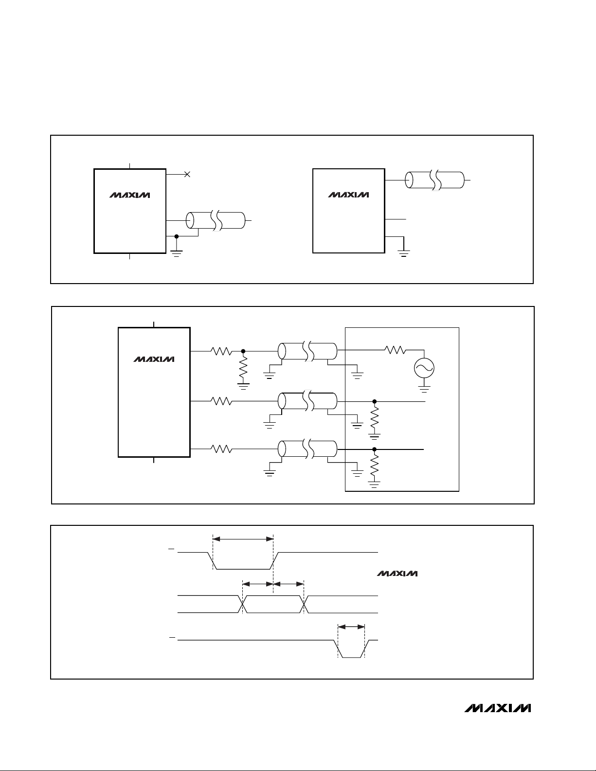
Figure 1. Turn-On/Turn-Off Time
Figure 2. Break-Before-Make Time Delay
Figure 3. Charge Injection
LE/CS
SER/PAR
A0
V+
V+
MAX4588
V-
NO_
NO_
COM_
GND
V
300Ω
NO_
V
OUT
30pF
V
GND
OUT
A0
90%
t
BBM
V-
MAX4588
Low-Voltage, High-Isolation,
Dual 4-Channel RF/Video Multiplexer
12 ______________________________________________________________________________________
V+
V+
V-
V-
1MHz
CAPACITANCE
ANALYZER
NO_
FLOATING
COM_
MAX4588
GND
FLOATING
1MHz
CAPACITANCE
ANALYZER
NO_
COM_
MAX4588
GND
Figure 4. NO_, COM_ Capacitance
Figure 5. Off-Isolation, Crosstalk, and Bandwidth
Figure 6. Parallel Timing Diagram
V+
V+
NO_
MAX4588
NO_
COM_
VV-
ALL SIGNALS NORMALIZED TO V
COM
= 0dB.
LE
A0, A1, A2, EN
49.9Ω
24.9Ω
560Ω
56Ω
50Ω
50Ω
50Ω
t
L
t
t
DS
DH
t
RS
MAX4588
+
-
MEASURE
NODE
MEASURE
NODE
RS
AND tF <10ns. TIMING IS MEASURED FROM 50% OF DIGITAL SIGNAL.
R
NOTE: ALL INPUT SIGNALS ARE SPECIFIED WITH t
Detailed Description
Logic-Level Translators
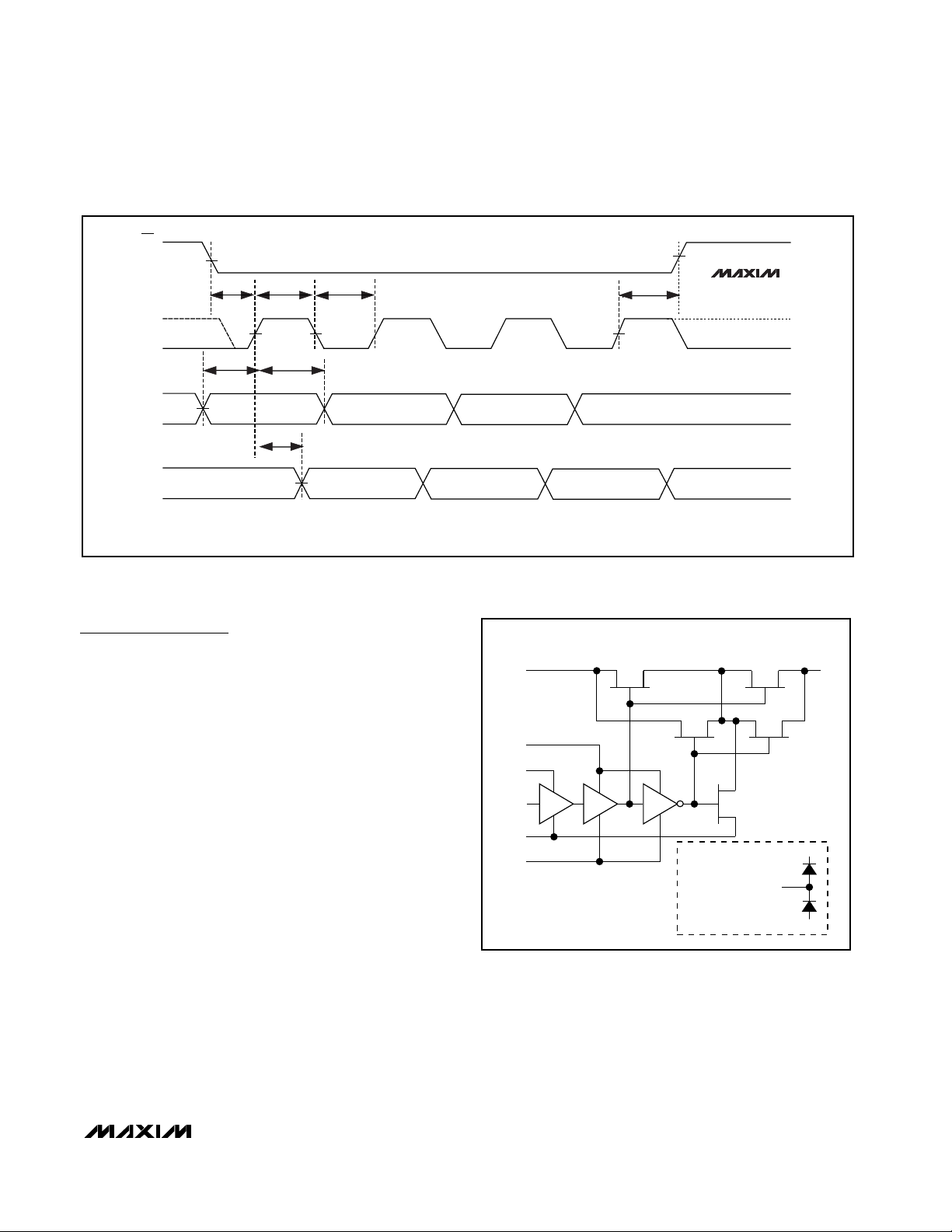
The MAX4588 is constructed of high-frequency “T”
switches, as shown in Figure 8. The logic-level inputs
are translated by amplifier A1 into a V+ to V- logic signal that drives amplifier A2. Amplifier A2 drives the
gates of N-channel MOSFETs N1 and N2 from V+ to V-,
turning them fully on or off. The same signal drives
inverter A3 (which drives the P-channel MOSFETs P1
and P2, turning them fully on or off) from V+ to V-, and
turns the N-channel MOSFET N3 on and off. The logiclevel threshold is determined by VLand GND.
Switch On Condition
When the switch is on, MOSFETs N1, N2, P1, and P2
are on and MOSFET N3 is off (Figure 8). The signal
path is COM_ to NO_, and because both N-channel
and P-channel MOSFETs act as pure resistances, it is
symmetrical (i.e., signals may pass in either direction).
The off MOSFET, N3, has no DC conduction, but has a
small amount of capacitance to GND. The four on
MOSFETs also have capacitance to ground that,
together with the series resistance, forms a lowpass filter. All of these capacitances are distributed evenly
along the series resistance, so they act as a transmission line rather than a simple R-C filter. The MAX4588’s
construction allows an exceptional 180MHz bandwidth
when the switches are on.
Typical attenuation in 75Ω systems is 2.5dB and is reasonably flat up to 50MHz. Higher-impedance circuits
show even lower attenuation (and vice versa), but
slightly lower bandwidth due to the increased effect of
the internal and external capacitance and the switch’s
internal resistance.
MAX4588
Low-Voltage, High-Isolation,
Dual 4-Channel RF/Video Multiplexer
______________________________________________________________________________________ 13
A1 A2 A3
P1
N3
N1
V-
GND
INPUT
V
CC
V+
V+
V+
COM_ NO_
N2
P2
NORMALLY OPEN SWITCH CONSTRUCTION
ESD DIODES
ON GND, NO_,
AND COM_
Figure 7. Serial Timing Diagram
Figure 8. T-Switch Construction
CS
t
CSS
SCLK
t
DS
DIN
DOUT
NOTE: ALL INPUT SIGNALS ARE SPECIFIED WITH t
TIMING IS MEASURED FROM 50% OF DIGITAL SIGNAL.
t
CH
t
DH
A0
t
DO
t
CL
A1
AND tF < 10ns.
R
A2 DISABLE
t
CSH
MAX4588

MAX4588
The MAX4588 is optimized for ±5V operation. Using
lower supply voltages or a single supply increases
switching time, on-resistance (and therefore on-state
attenuation), and nonlinearity.
Switch Off Condition
When the switch is off, MOSFETs N1, N2, P1, and P2
are off and MOSFET N3 is on (Figure 8). The signal
path is through the parasitic off-capacitances of the
series MOSFETs, but it is shunted to ground by N3.
This forms a highpass filter whose exact characteristics
are dependent on the source and load impedances. In
75Ω systems, and below 10MHz, the attenuation can
exceed 80dB. This value decreases with increasing frequency and increasing circuit impedances. External
capacitance and board layout have a major role in
determining overall performance.
Applications Information
Power-Supply Considerations
Overview
The MAX4588 construction is typical of many CMOS
analog switches. It has four supply pins: V+, V-, VL, and
GND. V+ and V- are used to drive the internal CMOS
switches and set the limits of the analog voltage on any
switch. Reverse ESD-protection diodes are internally
connected between each analog signal pin and both
V+ and V-. If the voltage on any pin exceeds V+ or V-,
one of these diodes will conduct. During normal operation these reverse-biased ESD diodes leak, forming the
only current drawn from V- and V+.
Virtually all the analog leakage current is through the
ESD diodes. Although the ESD diodes on a given signal pin are identical, and therefore fairly well balanced,
they are reverse-biased differently. Each is biased by
either V+ or V- and the analog signal. This means their
leakages vary as the signal varies. The difference in the
two diode leakages from the signal path to the V+ and
V- pins constitutes the analog signal-path leakage current. All analog leakage current flows to the supply terminals, not to the other switch terminal. This explains
how both sides of a given switch can show leakage
currents of either the same or opposite polarity.
There is no connection between the analog signal
paths and GND. The analog signal paths consist of an
N-channel and P-channel MOSFET with their sources
and drains paralleled and their gates driven out of
phase with V+ and V- by the logic-level translators.
VLand GND power the internal logic and logic-level
translators, and set the input logic thresholds. The
logic-level translators convert the logic levels to
switched V+ and V- signals to drive the gates of the
analog switches. This drive signal is the only connection between the logic supplies and the analog supplies.
Bipolar-Supply Operation
The MAX4588 operates with bipolar supplies between
±2.7V and ±6V. The V+ and V- supplies are not required
to be symmetrical, but their sum cannot exceed the
absolute maximum rating of 13.0V. Do not connect the
MAX4588 V+ pin to +3V and connect the logic-level
input pins to +5V logic-level signals. This level
exceeds the absolute maximum ratings, and may
cause damage to the part and/or external circuits.
CAUTION: The absolute maximum V+ to V- differential voltage is 13.0V. Typical “±6-Volt” or “12-Volt”
supplies with ±10% tolerances can be as high as
13.2V. This voltage can damage the MAX4588. Even
±5% tolerance supplies may have overshoot or
noise spikes that exceed 13.0V.
Single-Supply Operation
The MAX4588 operates from a single supply between
+2.7V and +12V when V- is connected to GND.
Observe all of the precautions listed in the
Bipolar-
Supply Operation
section. Note, however, that these
parts are optimized for ±5V operation, and AC and DC
characteristics are degraded significantly when operating at less than ±5V. As the overall supply voltage (V+
to V-) is reduced, switching speed, on-resistance, offisolation, and distortion are degraded (see
Typical
Operating Characteristics
).
Single-supply operation also limits signal levels and
interferes with grounded signals. When V- = 0, AC signals are limited to -0.3V. Voltages below -0.3V can be
clipped by the internal ESD-protection diodes, and the
parts can be damaged if excessive current flows.
Power Off
When power to the MAX4588 is off (i.e., V+ = 0 and V= 0), the
Absolute Maximum Ratings
still apply. This
means that none of the MAX4588 pins can exceed
±0.3V. Voltages beyond ±0.3V cause the internal ESDprotection diodes to conduct, with potentially catastrophic consequences.
Power-Supply Sequencing
When applying power to the MAX4588, follow this
sequence: V+, V- (if biased to potential other than
ground), VL, then logic inputs. Apply signals on the
analog NO_ and COM_ pins any time after V+, V-, and
GND voltages are set. Turning on all pins simultaneously is acceptable only if the circuit design guarantees
concurrent power-up.
Low-Voltage, High-Isolation,
Dual 4-Channel RF/Video Multiplexer
14 ______________________________________________________________________________________

The power-down sequence is the opposite of the
power-up sequence. That is, the VLand logic inputs
must go to zero potential before (or simultaneously
with) the V- then V+ supplies. The
Absolute Maximum
Ratings
must always be observed in order to ensure
proper operation.
Grounding
DC Ground Considerations
Satisfactory high-frequency operation requires that
careful consideration be given to grounding. For most
applications, a ground plane is strongly recommended, and all GND pins must connect to it with
solid copper. While the V+ and V- power-supply pins
are common to all switches in a given package, each
input is separated with ground pins that are not internally connected to each other. This contributes to the
overall high-frequency performance by reducing channel-to-channel crosstalk. All the GND pins have ESD
diodes to V+ and V-.
In systems that have separate digital and analog (signal) grounds, connect all GND pins to analog signal
ground. Preserving a good signal ground is much more
important than preserving a digital ground. Ground current is only a few nanoamperes.
The digital inputs have voltage thresholds determined by
VLand GND (V- does not influence the logic-level threshold). With +5V applied to VL, the threshold is about 1.6V,
ensuring compatibility with TTL- and CMOS-logic drivers.
AC Ground and Bypassing
A ground plane is mandatory for satisfactory highfrequency operation. Prototyping using hand wiring or
wire-wrap boards is not recommended. Connect all
GND pins to the ground plane with solid copper. (The
GND pins extend the high-frequency ground through
the package wire-frame, into the silicon itself, thus
improving isolation.) Make the ground plane solid metal
underneath the device, without interruptions. There
should be no traces under the device itself. For DIP
packages, this applies to both sides of a two-sided
board. Failure to observe this has a minimal effect on
the “on” characteristics of the switch at high frequencies, but will degrade the off-isolation and crosstalk.
When using the MAX4588’s SO package on PC boards
with a buried ground plane, connect each GND pin to the
ground plane with a separate via. Do not share this via
with any other ground path. Providing a ground via on
both sides of the SMT land further enhances the off-isolation by lowering the parasitic inductance. The DIP package can have the through-holes directly tied to the buried
plane, or thermally relieved as required to meet manufac-
turability requirements. Again, do not use the throughhole pads as the current path for any other components.
Bypass all V+ and V- pins to the ground plane with surface-mount 0.01µF capacitors. Locate these capacitors
as close as possible to the pins on the same side of the
board as the device. Do not use feedthroughs or vias
for bypass capacitors. If board layout dictates that the
bypass capacitors are mounted on the opposite side of
the PC board, use short feedthroughs or vias, directly
under the V+ and V- pins. Use multiple vias if possible.
If V- is 0, connect it directly to the ground plane with
solid copper. Keep all traces short.
Signal Routing
Keep all signal leads as short as possible. Separate all
signal leads from each other, and keep them away from
any other traces that could induce interference.
Separating the signal traces with generously sized
ground wires also helps minimize interference. Routing
signals via coaxial cable, terminated as close to the
MAX4588 as possible, provides the highest isolation.
Board Layout
IC sockets degrade high-frequency performance and
should not be used if signal bandwidth exceeds 5MHz.
Surface-mount parts, having shorter internal lead
frames, provide the best high-frequency performance.
Keep all bypass capacitors close to the device, and
separate all signal leads with ground planes. Such
grounds tend to be wedge-shaped as they get closer to
the device. Use vias to connect the ground planes on
each side of the board, and place the vias in the apex of
the wedge-shaped grounds that separate signal leads.
Logic-level signal lead placement is not critical.
Impedance Matching
The MAX4588 is intended for use in 75Ω systems,
where the inputs are terminated external to the IC and
the COM terminals see an impedance of 600Ω or higher. The MAX4588 can operate in 50Ω and 75Ω systems
with terminations through the IC. However, variations in
RONand RONflatness cause nonlinearities.
Crosstalk and Off-Isolation
The graphs shown in
Typical Operating Characteristics
for crosstalk and off-isolation are taken on adjacent
channels. The adjacent channel is the worst-case condition. For example, NO1 has the worst off-isolation to
COM1 due to their proximity. Furthermore, NO1 has the
most crosstalk to NO2, and the least crosstalk to NO4.
Choosing channels wisely necessitates separating the
most sensitive channels from the most offensive.
Conversely, the above information also applies to the
NO5–NO8 inputs to the COM2 pin.
MAX4588
Low-Voltage, High-Isolation,
Dual 4-Channel RF/Video Multiplexer
______________________________________________________________________________________ 15

MAX4588
Power-On Reset (POR)
The MAX4588 has internal circuitry to guarantee a
known state on power-up. In the default state, A0 = A1
= A2 = 0, disable = 1, and all switches are off. This
state is equivalent to asserting RS during normal operation.
Serial Operation
The serial mode is activated by driving the SER/PAR
input pin to a logic high. The data is then entered using a
normal SPI/MICROWIRE write operation. Refer to Figure
7 for a detailed diagram of the serial-interface logic.
There are four flip-flops in the shift register, with the output of the fourth shift register being output on the DOUT
pin. Note: DOUT changes on the rising edge of SCLK.
This allows cascading of multiple MAX4588s using only
one chip-select line. For example, one 16-bit write could
load the shift registers of four cascaded MAX4588s. The
data from the shift register is moved to the internal control latches only upon the rising edge of CS, so all four
MAX4588s change state simultaneously.
Parallel Operation
The parallel mode is activated by driving SER/PAR to a
logic low. The MAX4588 is programmed by a latched
parallel bus scheme. Refer to Figure 6 for a detailed
diagram of the parallel-interface logic. Note that 4/8 is
not latched. It is best to hard-wire 4/8 to a known state
for the desired mode of operation, or to use a dedicated microcontroller port pin.
Low-Voltage, High-Isolation,
Dual 4-Channel RF/Video Multiplexer
16 ______________________________________________________________________________________
Parallel Operation
Connects NO5 to COM210
Connects NO6 to COM210
Connects NO7 to COM210
Connects NO8 to COM210
Connect NO1 to COM1 and NO5 to COM2x0
Connects NO1 to COM100
Connects NO2 to COM100
Connects NO3 to COM100
Connects NO4 to COM100
All switches off.x0
Serial Mode. Refer to
Serial Operation
Truth Table
.
x1
SER/PAR
All switches off, latches are cleared.xx
Maintain previous state.x0
SWITCH STATESA2
0
0
1
1
0
0
0
1
1
x
x
x
x
A1
0
1
0
1
0
0
1
0
1
x
x
x
x
A0
1
1
1
1
1
1
1
1
1
0
x
x
x
EN
0
0
0
0
0
0
0
0
0
0
x
x
1
LE
1
1
1
1
1
1
1
1
1
1
1
0
1
RS
0
0
0
0
1
0
0
0
0
x
x
x
x
4/
88
Connect NO2 to COM1 and NO6 to COM2x0
Connect NO3 to COM1 and NO7 to COM2x0
Connect NO4 to COM1 and NO8 to COM2x0
0
1
1
1
0
1
1
1
1
0
0
0
1
1
1
1
1
1
x = Don’t Care
Note: 4/8 is not latched when LE is high. When LE is low, all latches are transparent. A2, A1, A0, and EN are latched.
Connect COM1 to COM2 externally for 1-of-8 single-ended operation.
Truth Tables

MAX4588
Low-Voltage, High-Isolation,
Dual 4-Channel RF/Video Multiplexer
______________________________________________________________________________________ 17
Serial Operation
Contents of shift register transferred to control
latches.
1 x x 1 1 *
Input shift register loads one bit from DIN. DOUT
updates on SCLK’s rising edge.
01
Input shift register loads one bit from DIN. DOUT
updates on SCLK’s rising edge.
01
Chip unselected.11
All switches off.x1
SER/PAR
Parallel Mode. Refer to
Parallel Operation Truth
Table.
x0
All switches off. Latches and shift register are
cleared. This is the power-on reset (POR) state.
x1
ON SWITCHES/STATES
CS
x
x
x
x
SCLK
0
1
x
x
x
x
DIN
1
1
1
0
x
x
EN
1
1
1
1
x
0
RS
*
*
*
*
High-Z
0
DOUT
Control Bit and 4/8 Logic
Connect NO5 to COM210
Connect NO6 to COM210
Connect NO7 to COM210
Connect NO8 to COM210
Connect NO1 to COM1 and NO5 to COM2x0
Connect NO1 to COM100
Connect NO2 to COM100
Connect NO3 to COM100
Connect NO4 to COM100
All switches off.x1
DISABLE
BIT
ON SWITCHES/STATES
A2
BIT
0
0
1
1
0
0
0
1
1
x
A1
BIT
0
1
0
1
0
0
1
0
1
x
A0
BIT
0
0
0
0
1
0
0
0
0
x
4/
88
PIN
Connect NO2 to COM1 and NO6 to COM2x0
Connect NO3 to COM2 and NO7 to COM2x0
Connect NO4 to COM2 and NO8 to COM2x0
0
1
1
1
0
1
1
1
1
x = Don’t Care
*
DOUT is delayed by 4 clock cycles from DIN.
x = Don’t Care
Note: DISABLE, A2, A1, and A0 are the 4 bits latched into the MAX4588 with a MICROWIRE/SPI write. A0 is the LSB (first bit in
time). DISABLE is the MSB (last bit in time).
Truth Tables (continued)

MAX4588
Low-Voltage, High-Isolation,
Dual 4-Channel RF/Video Multiplexer
18 ______________________________________________________________________________________
TRANSISTOR COUNT: 1033
____________________Chip Information
Package Information
28LNPDIP.EPS

MAX4588
Low-Voltage, High-Isolation,
Dual 4-Channel RF/Video Multiplexer
______________________________________________________________________________________ 19
Package Information (continued)
SOICW.EPS

MAX4588
Low-Voltage, High-Isolation,
Dual 4-Channel RF/Video Multiplexer
Maxim cannot assume responsibility for use of any circuitry other than circuitry entirely embodied in a Maxim product. No circuit patent licenses are
implied. Maxim reserves the right to change the circuitry and specifications without notice at any time.
20
____________________Maxim Integrated Products, 120 San Gabriel Drive, Sunnyvale, CA 94086 408-737-7600
© 1999 Maxim Integrated Products Printed USA is a registered trademark of Maxim Integrated Products.
Package Information (continued)
SSOP.EPS
 Loading...