

Page 1
For free samples & the latest literature: http://www.maxim-ic.com, or phone 1-800-998-8800.
For small orders, phone 1-800-835-8769.
General Description
The MAX4586/MAX4587 serial-interface, programmable,
4-to-1 channel multiplexers are ideal for multimedia
applications. They feature 65Ω on-resistance, 4Ω on-
resistance matching between channels, and 5Ω onresistance flatness. Additionally, they feature -83dB
off-isolation at 20kHz and -48dB off-isolation at 10MHz,
with -84dB crosstalk at 20kHz and -60dB crosstalk at
10MHz.
The MAX4586 uses a 2-wire, I2C™-compatible serial
interface; the MAX4587 uses a 3-wire, SPI™/QSPI™/
MICROWIRE™-compatible interface. Both devices are
available in 10-pin µMAX packages and are specified
for the extended -40°C to +85°C temperature range.
Applications
Cellular Phones and Accessories
Private Mobile Radios (PMRs)
PC Multimedia Audio/Video Routing
Industrial Equipment
Set-Top Boxes
Video Conferencing
High-End Audio Equipment
Features
♦ +2.7V to +5.5V Single-Supply Operation
♦ 4-to-1 Channel Multiplexer
♦ 65Ω (max) R
ON
with +5V Supply
♦ Audio Performance
-83dB Off-Isolation at 20kHz
-84dB Crosstalk at 20kHz
♦ Video Performance
-48dB Off-Isolation at 10MHz
-60dB Crosstalk at 10MHz
♦ Serial Interface
2-Wire, I
2
C Compatible (MAX4586)
3-Wire, SPI/QSPI/MICROWIRE Compatible
(MAX4587)
MAX4586/MAX4587
Serially Controlled, 4-Channel
Audio/Video Multiplexers
________________________________________________________________
Maxim Integrated Products
1
19-1511; Rev 0; 8/99
PART
MAX4586EUB
MAX4587EUB
-40°C to +85°C
-40°C to +85°C
TEMP. RANGE PIN-PACKAGE
10 µMAX
10 µMAX
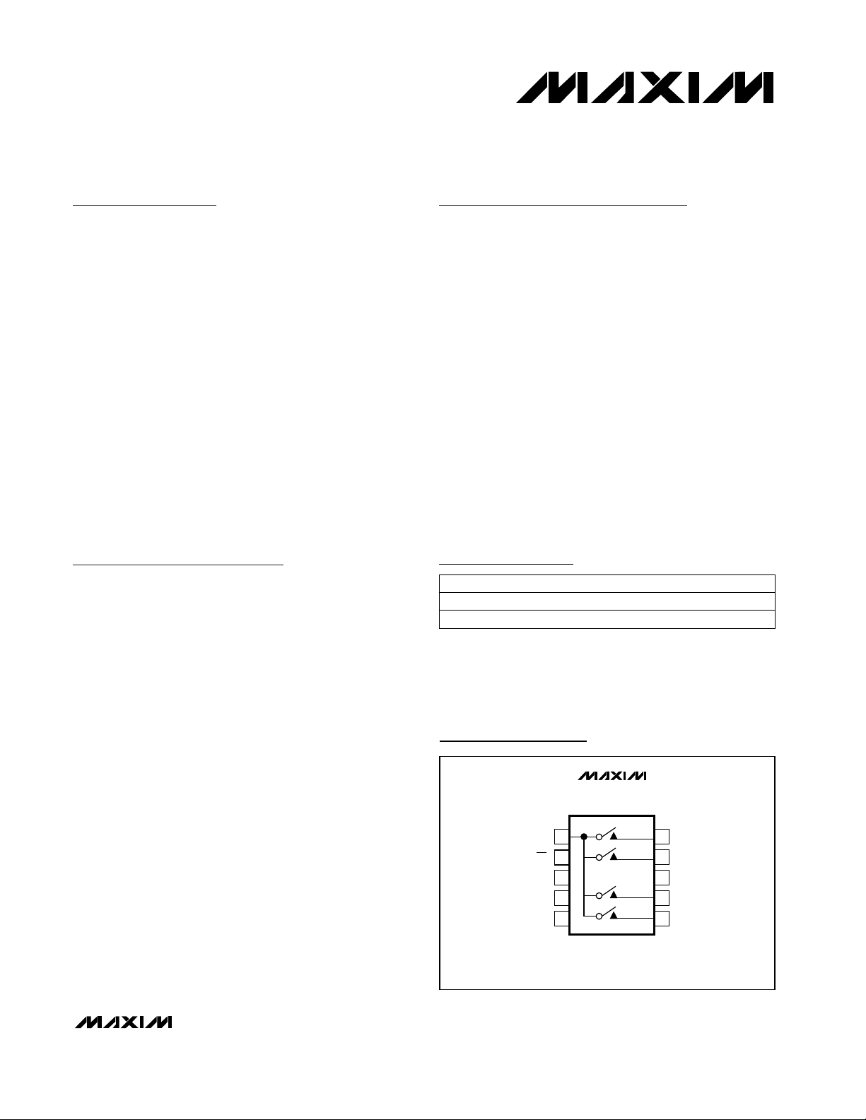
Pin Configuration/
Functional Diagram
Ordering Information
I2C is a trademark of Philips Corp.
SPI/QSPI are trademarks of Motorola, Inc.
MICROWIRE is a trademark of National Semiconductor Corp.
TOP VIEW
MAX4586
MAX4587
COM
A (CS)
SDA (DIN)
V+
SCL(SCLK)
( ) ARE FOR MAX4587 ONLY.
1
2
3
4
5
µMAX
10
NO4
9
NO3
GND
8
7
NO2
NO1
6
Page 2
MAX4586/MAX4587
Serially Controlled, 4-Channel
Audio/Video Multiplexers
2 _______________________________________________________________________________________
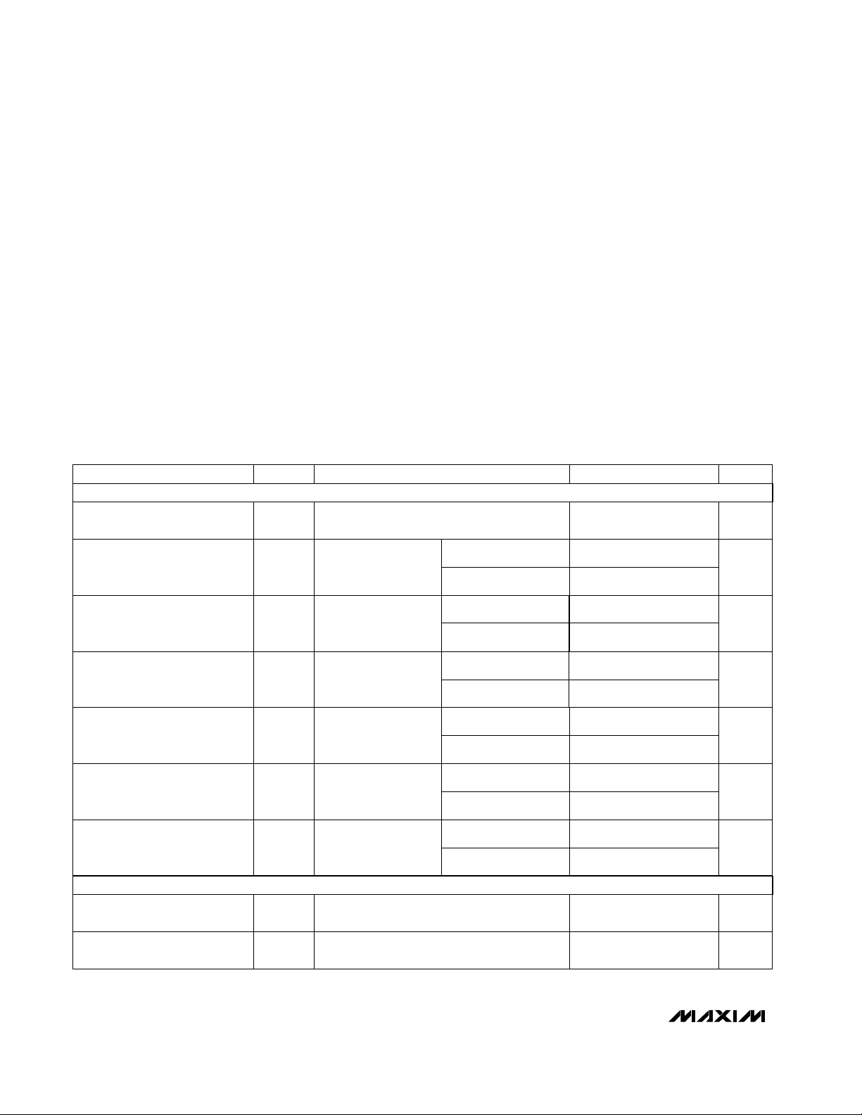
ABSOLUTE MAXIMUM RATINGS
ELECTRICAL CHARACTERISTICS—Single +5V Supply
(V+ = +5V ±5%, TA= T
MIN
to T
MA
X
, unless otherwise noted. Typical values are at TA= +25°C.) (Note 2)
Stresses beyond those listed under “Absolute Maximum Ratings” may cause permanent damage to the device. These are stress ratings only, and functional
operation of the device at these or any other conditions beyond those indicated in the operational sections of the specifications is not implied. Exposure to
absolute maximum rating conditions for extended periods may affect device reliability.
V+ to GND................................................................-0.3V to +6V
COM and NO_ to GND (Note 1)...................-0.3V to (V+ + 0.3V)
A, CS, SDA, DIN, SCL, and SCLK to GND...............-0.3V to +6V
Continuous Current into Any Terminal..............................±20mA
Peak Current into Any Terminal
(pulsed at 1ms, 10% duty cycle).................................±40mA
ESD per Method 3015.7.......................................................>2kV
Continuous Power Dissipation (T
A
= +70°C)
10-Pin µMAX (derate 4.1mW/°C above +70°C) ..........330mW
Operating Temperature Range ...........................-40°C to +85°C
Storage Temperature Range .............................-65°C to +150°C
Lead Temperature (soldering, 10sec) .............................+300°C
Note 1: Signals on NO_ or COM exceeding V+ or ground are clamped by internal diodes. Limit forward-diode current to maximum
current rating.
VA= 1.0V
RMS
, fIN= 20kHz, RS= 600Ω,
Figure 8
dB
TA= +25°C
VA= 1.0V
RMS
, fIN= 20kHz, RL= 600Ω,
Figure 8
TA= T
MIN
to T
MAX
TA= +25°C
CONDITIONS
-84V
CT(A)
Channel-to-Channel Crosstalk
24
V0V+
V
NO_
,
V
COM
Analog Signal Range (Note 3)
dB-83V
ISO(A)
Off-Isolation (Note 7)
5
TA= +25°C
TA= T
MIN
to T
MAX
TA= +25°C
TA= T
MIN
to T
MAX
-1 0.001 1
45 65
80
-10 10
TA= T
MIN
to T
MAX
UNITSMIN TYP MAXSYMBOLPARAMETER
25
6.5
V+ = 5.25V; V
NO_
=
1V, 4.5V, or floating;
V
COM
= 1V, 4.5V
TA= +25°C
TA= +25°C
nAI
COM(ON)
COM On-Leakage Current
(Note 6)
-1 0.002 1
TA= T
MIN
to T
MAX
-1 0.001 1
-10 10
V+ = 4.75V,
V
NO_
= 3V,
I
COM
= 4mA
R
ON
On-Resistance Ω
Ω
V+ = 4.75V,
V
NO_
= 3V,
I
COM
= 4mA
∆R
ON
On-Resistance Match
Between Channels
(Note 4)
Ω
V+ = 4.75V;
V
NO_
= 1V, 2V, 3V;
I
COM
= 4mA
R
FLAT
On-Resistance Flatness
(Note 5)
nA
V+ = 5.25V;
V
NO_
= 1V, 4.5V;
V
COM
= 4.5V, 1V
I
NO_(OFF)
NO_ Off-Leakage Current
(Note 6)
TA= T
MIN
to T
MAX
-10 10
AUDIO PERFORMANCE
ANALOG SWITCHES
nA
V+ = 5.25V;
V
NO_
= 1V, 4.5V;
V
COM
= 4.5V, 1V
I
COM(OFF)
COM Off-Leakage Current
(Note 6)
Page 3
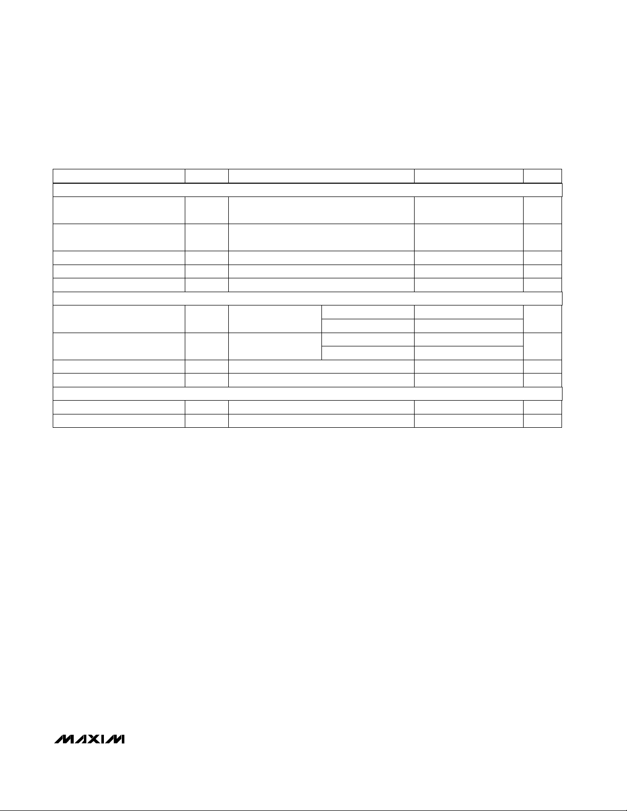
Serially Controlled, 4-Channel
Audio/Video Multiplexers
_______________________________________________________________________________________ 3
MAX4586/MAX4587
ELECTRICAL CHARACTERISTICS—Single +5V Supply (continued)
(V+ = +5V ±5%, TA= T
MIN
to T
MAX
, unless otherwise noted. Typical values are at TA= +25°C.) (Note 2)
T
A
= T
MIN
to T
MAX
TA= +25°C
TA= T
MIN
to T
MAX
TA= +25°C
250
V
NO_
= 2.5V,
RL= 300Ω, CL= 35pF
ns
125 200
t
OFF
Turn-Off Time
500
V
NO_
= 2.5V,
RL= 5kΩ, CL= 35pF
ns
275 400
t
ON
Turn-On Time
All logic inputs = 0 or V+
CL= 1.0nF, VS= 0, RS= 0, Figure 7
fIN= 1MHz
CONDITIONS
VA= 1.0V
RMS
, fIN= 10MHz, RS= 50Ω,
Figure 8
dB-60V
CT(V)
Channel-to-Channel Crosstalk
µA510I+Supply Current
V2.7 5.5V+Power-Supply Voltage Range
pC3QCharge Injection
V
NO_
= 2.5V, Figure 6 ns10 50t
BBM
Break-Before-Make Time
pF5C
OFF
NO_ Off-Capacitance
UNITSMIN TYP MAXSYMBOLPARAMETER
RS= 75Ω, RL= 1kΩ
RS= 50Ω, RL= 50Ω MHz300BW-3dB Bandwidth
MHz5BW-0.1dB Bandwidth
VA= 1.0V
RMS
, fIN= 10MHz, RL= 50Ω,
Figure 8
dB-48V
ISO(V)
Off-Isolation (Note 7)
VIDEO PERFORMANCE
DYNAMIC TIMING (Notes 8, 9, and Figure 5)
POWER SUPPLY
Page 4
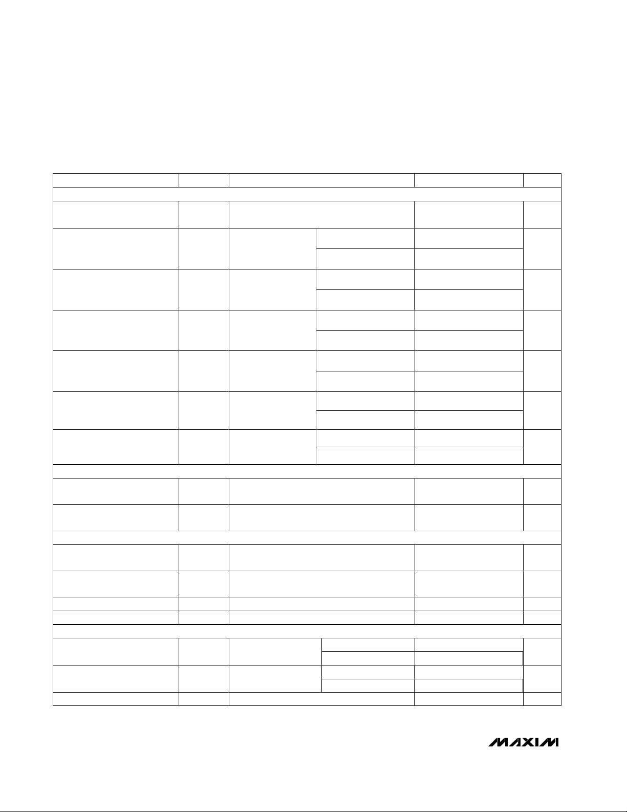
MAX4586/MAX4587
Serially Controlled, 4-Channel
Audio/Video Multiplexers
4 _______________________________________________________________________________________
ELECTRICAL CHARACTERISTICS—Single +3V Supply
(V+ = +3V ±10%, TA= T
MIN
to T
MAX
, unless otherwise noted. Typical values are at TA= +25°C.)
T
A
= +25°C
TA= T
MIN
to T
MAX
130
On-Resistance R
ON
V+ = 2.7V,
V
NO_
= 1V,
I
COM
= 4mA
65 110
Ω
Analog Signal Range (Note 3)
V
NO_
,
V
COM
0V+V
TA= +25°C
TA= T
MIN
to T
MAX
12
On-Resistance Flatness
(Note 5)
R
FLAT
V+ = 2.7V;
V
NO_
= 1V, 1.5V, 2V;
I
COM
= 4mA
310
Ω
ns
TA= +25°C
TA= +25°C
TA= T
MIN
to T
MAX
-10 10
TA= T
MIN
to T
MAX
CONDITIONS
COM On-Leakage Current
(Notes 6, 10)
I
COM(ON)
V+ = 3.6V; V
NO_
=
0.5V, 3V, or floating;
V
COM
= 0.5V, 3V
-1 0.002 1
nA
Off-Isolation (Note 7) V
ISO(A)
VA= 0.5V
RMS
, fIN= 20kHz, RL= 600Ω,
Figure 8
-83 dB
Channel-to-Channel Crosstalk V
CT(A)
VA= 0.5V
RMS
, fIN= 20kHz, RS= 600Ω,
Figure 8
-84 dB
UNITSMIN TYP MAXSYMBOLPARAMETER
Off-Isolation (Note 7) V
ISO(V)
VA= 0.5V
RMS
, fIN= 10MHz, RL= 50Ω,
Figure 8
-48 dB
Channel-to-Channel Crosstalk V
CT(V)
VA= 0.5V
RMS
, fIN= 10MHz, RS= 50Ω,
Figure 8
-60 dB
NO_ Off-Capacitance C
OFF
fIN= 1MHz 5 pF
Turn-On Time t
ON
V
NO_
= 1.5V,
RL= 5kΩ, CL= 35pF
400 800
ns
1000
TA= +25°C
TA= T
MIN
to T
MAX
6
On-Resistance Match
Between Channels
(Note 4)
∆R
ON
V+ = 2.7V,
V
NO_
= 1V,
I
COM
= 4mA
35
Ω
TA= +25°C
TA= T
MIN
to T
MAX
Turn-Off Time t
OFF
V
NO_
= 1.5V,
RL= 300Ω, CL= 35pF
200 350
500
V
NO_
= 1.5V, Figure 6Break-Before-Make Time t
BBM
10 100 ns
TA= +25°C
TA= T
MIN
to T
MAX
-10 10
COM Off-Leakage Current
(Notes 6, 10)
I
COM(OFF)
V+ = 3.6V;
V
NO_
= 0.5V, 3V;
V
COM
= 3V, 0.5V
-1 0.001 1
nA
TA= +25°C
TA= T
MIN
to T
MAX
-10 10
NO_ Off-Leakage Current
(Notes 6, 10)
I
NO_(OFF)
V+ = 3.6V;
V
NO_
= 0.5V, 3V;
V
COM
= 3V, 0.5V
-1 0.001 1
nA
-3dB Bandwidth BW RS= 50Ω, RL= 50Ω 200 MHz
ANALOG SWITCHES
AUDIO PERFORMANCE
VIDEO PERFORMANCE
DYNAMIC TIMING (Notes 8, 9, and Figure 5)
Page 5

MAX4586/MAX4587
Serially Controlled, 4-Channel
Audio/Video Multiplexers
_______________________________________________________________________________________ 5
I/O INTERFACE CHARACTERISTICS
(V+ = +2.7V to +5.25V, TA= T
MIN
to T
MAX
, unless otherwise noted. Typical values are at TA= +25°C.)
2-WIRE TIMING CHARACTERISTICS
(Figures 1 and 2, V+ = +2.7V to +5.25V, f
SCL
= 100kHz, TA= T
MIN
to T
MAX
, unless otherwise noted. Typical values are at TA= +25°C.)
UNITSMIN TYP MAXCONDITIONSSYMBOLPARAMETER
ns
20 +
300
0.1C
B
t
R
SCL/SDA Rise Time (Note 11)
µs4.0t
HIGH
Clock High Period
µs4.7t
LOW
Clock Low Period
ns250t
SU:DAT
Data Setup Time
µs0t
HD:DAT
Data Hold Time
µs4.0t
SU:STO
Stop Condition Setup Time
µs4.7t
BUF
Bus Free Time Between Stop
and Start Condition
0 100V+ = 2.7V to 5.25V
f
SCL
SCL Clock Frequency
ns
20 +
300
0.1C
B
t
F
SCL/SDA Fall Time (Note 11)
µs4.0The first clock is generated after this period.t
HD:STA
Hold Time After Start Condition
kHz
400V+ = 4.75V to 5.25V
Output Low Voltage V
OL
I
SINK
= 6mA 0.4 V
Input Low Voltage V
IL
V+ = 5V 0.8
V
Input High Voltage V
IH
V+ = 5V 3
V
2
0.6V+ = 3V
V+ = 3V
Input Leakage Current I
LEAK
Digital inputs = 0 or V+ -1 0.01 1 µA
PARAMETER SYMBOL CONDITIONS MIN TYP MAX UNITS
Input Hysteresis V
HYST
0.2 V
Input Capacitance C
IN
f = 1MHz 5 pF
DIGITAL INPUTS (SCLK, DIN, CS, SCL, SDA, A)
DIGITAL OUTPUT (SDA)
Page 6

MAX4586/MAX4587
Serially Controlled, 4-Channel
Audio/Video Multiplexers
6 _______________________________________________________________________________________
3-WIRE TIMING CHARACTERISTICS
(Figures 3 and 4, V+ = +2.7V to +5.25V, fOP= 2.1MHz, TA= T
MIN
to T
MAX
, unless otherwise noted. Typical values are at TA= +25°C.)
ns
40t
CSW
CS Pulse Width High
UNITSMIN TYP MAXCONDITIONSSYMBOLPARAMETER
ns100t
CSS
CS Fall to SCLK Rise Setup
µs2
ns0t
DH
DIN to SCLK Hold
MHz
0 2.1V+ = 2.7V to 5.25V
f
OP
Operating Frequency
ns100t
DS
DIN to SCLK Setup
t
R
Rise Time (SCLK, DIN, CS)
ns0t
CSH
CS Rise to SCLK Hold
ns200t
CL
SCLK Pulse Width Low
µs2t
F
Fall Time (SCLK, DIN, CS)
ns
10V+ = 4.75V to 5.25V
200t
CH
SCLK Pulse Width High
Note 2: Algebraic convention is used in this data sheet; the most negative value is shown in the minimum column.
Note 3: Guaranteed by design. Not subject to production testing.
Note 4: ∆R
ON
= R
ON(MAX)
- R
ON(MIN)
.
Note 5: Resistance flatness is defined as the difference between the maximum and minimum on-resistance values, as measured
over the specified analog signal range.
Note 6: Leakage parameters are 100% tested at maximum rated temperature and guaranteed by correlation at T
A
= +25°C.
Note 7: Off-isolation = 20log (V
COM
/ VNO_ ), V
COM
= output, VNO_ = input to off switch.
Note 8: All timing is measured from the clock’s falling edge preceding the ACK signal for 2-wire and from the rising edge of CS for
3-wire. Turn-off time is defined at the output of the switch for a 0.5V change, tested with a 300Ω load to ground. Turn-on
time is defined at the output of the switch for a 0.5V change and measured with a 5kΩ load resistor to GND. All timing is
shown with respect to 20% V+ and 70% V+, unless otherwise noted.
Note 9: Typical values are for MAX4586 devices.
Note 10: Leakage testing is guaranteed by testing with a +5.25V supply.
Note 11: C
B
= capacitance of one bus line in pF. Tested with CB= 400pF.
V
COM
(V)
30
35
65
45
40
50
55
60
70
0 1.0 1.5 2.00.5 2.5 3.0 4.54.0 5.03.5 5.5
ON-RESISTANCE
vs. V
COM
AND SUPPLY VOLTAGE
MAX4586/7-01
R
ON
(Ω)
V+ = 2.7V
V+ = 3.0V
V+ = 4.0V
V+ = 5.0V
V+ = 5.5V
V
COM
(V)
30
50
40
35
45
55
0 1.0 1.5 2.0
0.5
2.5
3.0 4.54.0 5.03.5
ON-RESISTANCE vs.
V
COM
AND TEMPERATURE (V+ = 5V)
MAX4586/7-02
R
ON
(Ω)
TA = -40°C
TA = -55°C
TA = +125°C
TA = +85°C
TA = +25°C
V
COM
(V)
30
65
60
45
40
35
55
50
75
70
0
1.0
1.5
2.0
0.5
2.5
3.0
ON-RESISTANCE vs.
V
COM
AND TEMPERATURE (V+ = 3.3V)
MAX4586/7-03
R
ON
(Ω)
TA = -40°C
TA = -55°C
TA = +85°C
TA = +25°C
TA = +125°C
Typical Operating Characteristics
(V+ = +5V, TA = +25°C, unless otherwise noted.)
Page 7

MAX4586/MAX4587
Serially Controlled, 4-Channel
Audio/Video Multiplexers
_______________________________________________________________________________________
7
Typical Operating Characteristics (continued)
(V+ = +5V, TA = +25°C, unless otherwise noted.)
SUPPLY CURRENT vs. TEMPERATURE
5.0
4.9
4.8
4.7
4.6
4.5
4.4
4.3
SUPPLY CURRENT (µA)
4.2
4.1
4.0
-55 -15 5 25-35 45 65 85 105 125
TEMPERATURE (°C)
MAX4586/7-04
TURN-ON/TURN-OFF TIMES
vs. TEMPERATURE
350
300
250
200
TIME (ns)
150
100
50
t
ON
t
OFF
MAX4586/7-07
CURRENT (nA)
CHARGE INJECTION vs. V
3
2
1
0
-1
-2
CHARGE INJECTION (pC)
-3
-4
0 2.01.0 3.0 4.00.5 2.51.5 3.5 4.5 5.0
V
(V)
COM
ON-LEAKAGE CURRENT
vs. TEMPERATURE
0.01
10
0.1
I
@
COM(ON)
= 4.5V
V
COM
V
= FLOATING
1
NO
I
COM(ON)
V
COM
V
= FLOATING
NO
@
= 1.0V
COM
MAX4586/7-05
TIME (ns)
MAX4586/7-08A
CURRENT (nA)
0.01
TURN-ON AND TURN-OFF TIMES
vs. SUPPLY VOLTAGE
700
600
500
400
t
300
200
100
0
2.5 3.5 4.03.0 4.5 5.0 5.5
ON
t
OFF
SUPPLY VOLTAGE (V)
OFF-LEAKAGE CURRENT
vs. TEMPERATURE
10
1
I
NO(OFF)
V
NO
V
COM
0.1
I
NO(OFF)
V
NO
V
COM
= 4.5V
= 1.0V
= 1.0V
= 4.5V
I
COM(OFF)
V
COM
= 4.5V
V
NO
@
@
= 1.0V
I
@
COM(OFF)
V
COM
V
NO
= 4.5V
= 1.0V
@
MAX4586/7-06
MAX4586/7-08B
0
-55 -15 5-35 25 45 65 85 105 125
TEMPERATURE (°C)
AUDIO FREQUENCY RESPONSE
0
600Ω IN AND OUT
-10
-20
-30
-40
-50
LOSS (dB)
-60
-70
-80
-90
-100
0.01 1 100.1 100
FREQUENCY (kHz)
OFF-ISOLATION
CROSSTALK
MAX4586/7-09
0.001
0
-10
-20
-30
-40
-50
LOSS (dB)
-60
-70
-80
-90
-100
25
-55 5-15
-35 65 125
45 85
TEMPERATURE (°C)
VIDEO FREQUENCY RESPONSE
INSERTION LOSS
OFF-ISOLATION
CROSSTALK
50Ω IN AND OUT
0.1 100101
FREQUENCY (MHz)
105
MAX4586/7-10
0.001
5V/div
2V/div
2V/div
25
-55 5-15
-35 65 125
45 85
TEMPERATURE (°C)
TURN-ON/TURN-OFF TIMES
CLK
t
ON
t
OFF
100ns/div
105
MAX4586/7-11
Page 8

MAX4586/MAX4587
Detailed Description
The MAX4586/MAX4587 are serial-interface, programmable multiplexers. Each device contains a 4-to-1 normally
open (NO) multiplexer. Each switch is independently controlled through the on-chip serial interface. The MAX4586
uses a 2-wire, I2C-compatible serial communications
protocol, and the MAX4587 uses a 3-wire, SPI/QSPI/
MICROWIRE-compatible serial communications protocol.
These devices operate from a single +2.7V to +5.5V
supply and are optimized for use with an audio frequency at 20kHz and video frequencies up to 10MHz.
They feature 65Ω on-resistance, 4Ω on-resistance
matching between channels, and 5Ω on-resistance flatness. Audio off-isolation is -83dB at 20kHz and
crosstalk is at least -84dB at 20kHz, while video off-isolation is -48dB at 10MHz and crosstalk is at least -60dB
at 10MHz.
Applications Information
Multiplexer Control
The MAX4586/MAX4587 have a common command-bit
structure; the only difference between them is the interface type (2-wire or 3-wire, respectively).
The command controls the open/closed states of the
various switches. Table 1 shows the configuration of
the data bits and their related switches. After a command is issued, a logic “1” in any data-bit location closes the associated switch, while a logic “0” opens it
(Table 2).
2-Wire Serial Interface
The MAX4586 uses a 2-wire, I2C-compatible serial
interface. The COM_ register uses the “SendByte” protocol that consists of an address byte followed by a
command byte (Table 1).
To address a given chip, the A bit in the address byte
must duplicate the value present at the A pin of that chip.
The rest of the address bits must match those shown in
Table 3. The command byte details are described in the
Switch Control
section.
The 2-wire serial interface requires only two I/O lines of
a standard microprocessor (µP) port. Figures 1 and 2
detail the timing diagram for signals on the 2-wire bus,
and Tables 1 and 3 detail the format of the signals. The
MAX4586 is a receive-only device and must be controlled by the bus master device. A bus master device
communicates by transmitting the address byte of the
slave device over the bus and then transmitting the
desired information. Each transmission consists of a
start condition, an address byte, a command byte, and
finally a stop condition. The slave device acknowledges
the recognition of its address by pulling the SDA line
low for one clock period after the address byte is transmitted. The slave device also issues a similar acknowledgment after the command byte.
Serially Controlled, 4-Channel
Audio/Video Multiplexers
8 _______________________________________________________________________________________
Pin Description
9
8
9
7 7
— 5
4 4
8
6
—
3
—
2
—
1
NO3
NO2
6
SCLK
5
V+
COM1
SDA
GND
NO1
SCL
DIN
3
—
CS
—
A2
Mux Normally Open Output 3
Mux Normally Open Output 2
Clock Input of the 3-Wire Serial Interface
Supply Voltage
Analog Switch Common Terminal
Data Input of 2-Wire Serial Interface
Ground
Mux Normally Open Output 1
Clock Input of the 2-Wire Serial Interface
Data Input of 3-Wire Serial Interface
Chip Select of the 3-Wire Serial Interface
LSB + 2 of the 2-Wire Serial-Interface Address Field
10 10 NO4 Mux Normally Open Output 4
MAX4587MAX4586
PIN
NAME FUNCTION
Page 9

Start and Stop Conditions
The bus master signals the beginning of a transmission
with a start condition by transitioning SDA from high to
low while SCL is high. When the bus master has finished communicating with the slave device, it issues a
stop condition by transitioning SDA from low to high
while SCL is high. The bus master is then free for
another transmission.
Slave Address (Address Byte)
The MAX4586 uses an 8-bit-long slave address. To
select a slave address, connect A to V+ or GND. The
MAX4586 has two possible slave addresses, so a maximum of two of these devices may share the same
address line. The slave device MAX4586 monitors the
serial bus continuously, waiting for a start condition followed by an address byte. When a slave device recog-
MAX4586/MAX4587
Serially Controlled, 4-Channel
Audio/Video Multiplexers
_______________________________________________________________________________________ 9
Figure 1. 2-Wire Serial-Interface Timing Diagram
Table 1. Command-Bit Mapping
Table 3. Address Bit Map
Table 2. Truth Table
xxD4
xxD5
xxD6
xxD7 (MSB)
POWER-UP
STATE
TERMINALSSWITCH
COMMAND
BIT
0 (Open)6, 1NO1 to COMD0 (LSB)
0 (Open)7, 1NO2 to COMD1
0 (Open)9, 1NO3 to COMD2
0 (Open)10, 1NO4 to COMD3
CLOSED1
OPEN0
NO_ SWITCHLOGIC
0110 11101
0110 10100
ADDRESSADDRESS BIT (A)
Figure 2. Complete 2-Wire Serial-Interface Transmission
X = Don’t care
SDA
SCL
tHD,
STA
20%
70%
20%
t
LOW
70%
tSU,
DAT
70% 70%
20%
t
HIGH
t
R
70%
20%
t
F
tHD,
20%
DAT
70%
20%
tSU,
STA
70% 70% 70%
tHD,
STA
tSU,
STO
70%
20%
70%
20%
t
BUF
START CONDITIONSTOP CONDITIONREPEATED START CONDITIONSTART CONDITION
SLAVE ADDRESS BYTE
SDA
SCL
START CONDITION STOP CONDITION
MSB
LSB LSBACK ACK
COMMAND BYTE
MSB
Page 10

MAX4586/MAX4587
nizes its address (01101A10), it acknowledges that it is
ready for further communication by pulling the SDA line
low for one clock period.
3-Wire Serial Interface
The MAX4587 3-wire serial interface is SPI/QSPI/
MICROWIRE compatible. An active-low chip-select
(CS) input enables the device to receive data for the
serial input (DIN). Data is clocked in on the rising edge
of the serial-clock (SCLK) signal. A total of 8 bits is
needed in each write cycle. The first bit clocked into
the MAX4587 is the command byte’s MSB, and the last
bit clocked in is the data byte’s LSB. The first four bits
of the command byte are “don’t care.” While shifting
data, the device remains in its original configuration.
After all eight bits are clocked into the input shift register, a rising edge on CS latches the data into the
MAX4587 internal registers, initiating the device’s
change of state. Figures 3 and 4 detail the 3-wire protocol, and Table 1 details the command byte format.
Addressable Serial Interface
To program several MAX4587s individually using a single processor, connect DIN of each MAX4587 together
and control CS on each MAX4587 separately. To select
a particular device, drive the corresponding CS low,
clock in the 8-bit command, then drive CS high to execute the command. Typically, only one MAX4587 is
addressed at a time.
Power-Up State
The MAX4586/MAX4587 feature a preset power-up
state. See Table 1 to determine the power-up state of
the devices.
Serially Controlled, 4-Channel
Audio/Video Multiplexers
10 ______________________________________________________________________________________
Figure 3. 3-Wire Serial-Interface Timing Diagram
Figure 4. Complete 3-Wire Serial Transmission
TRANSISTOR COUNT: 2259
___________________Chip Information
CS
SCLK
DIN
CS
SCLK
DATA CLOCKED IN
DIN
D7 D6 D5 D4
MSB
20%
t
CSS
20% 20% 20% 20% 20%
t
DH
t
DS
D7
SWITCHES UPDATED
D3 D2 D1 D0
INPUT DATA BITS
t
CL
LSB
70%
70%
t
CSO
20%
t
t
CH
70%
D6
D1 D0
70%
CSH
t
CSW
Page 11

MAX4586/MAX4587
Serially Controlled, 4-Channel
Audio/Video Multiplexers
______________________________________________________________________________________ 11
Test Circuits/Timing Diagrams
Figure 6. Break-Before-Make Interval
Figure 5. Switching Time
MAX4586
MAX4587
V
NO_
2 OR 3
µP
CL INCLUDES FIXTURE AND STRAY CAPACITANCE.
[RL / (RL + R
= V
V
OUT
NO_
MAX4586
MAX4587
NO_
V
IN
NO_
2 OR 3
µP
NO_
DECODER/
CONTROLLER
SERIAL
INTERFACE
CONTROLLER
SERIAL
INTERFACE
V+
V+
GND
)]
ON
V+
V+
DECODER/
GND
10nF
COM
10nF
COM
ACKNOWLEDGE
3V
SCL
0
V
2-WIRE
V
OUT
C
R
L
L
35pF
3-WIRE
SCL
2-WIRE
V
OUT
C
R
L
L
CS
3-WIRE
OUT
0
V
OUT
0
3V
CS
0
V
OUT
0
V
OUT
0
3V
0V
V
OUT
0
3V
0
V
OUT
50%
50%
t
BBM
50%
0.5V
t
ON
V
OUT -
t
OFF
50%
0.5V
t
ON
V
t
OFF
ACKNOWLEDGE BIT
80%
80%
OUT
BIT
0.5V
- 0.5V
< 20ns
t
R
t
< 20ns
F
tR < 20ns
< 20ns
t
F
CL INCLUDES FIXTURE AND STRAY CAPACITANCE.
[RL / (RL + R
= V
V
OUT
COM_
)]
ON
0
t
BBM
Page 12

MAX4586/MAX4587
Serially Controlled, 4-Channel
Audio/Video Multiplexers
Figure 8. Off-Isolation and Crosstalk
Figure 7. Charge Injection
Test Circuits/Timing Diagrams (continued)
Maxim cannot assume responsibility for use of any circuitry other than circuitry entirely embodied in a Maxim product. No circuit patent licenses are
implied. Maxim reserves the right to change the circuitry and specifications without notice at any time.
12
____________________Maxim Integrated Products, 120 San Gabriel Drive, Sunnyvale, CA 94086 408-737-7600
© 1999 Maxim Integrated Products Printed USA is a registered trademark of Maxim Integrated Products.
V+
MAX4586
10nF
MAX4587
DECODER/
CONTROLLER
SERIAL
INTERFACE
V+
GND
COM
C
L
1000pF
NO_
2 OR 3
µP
∆V
IS THE MEASURED VOLTAGE DUE TO CHARGE-TRANSFER
OUT
ERROR Q WHEN THE CHANNEL TURNS OFF.
• C
Q = ∆V
OUT
L
V+
10nF
ACKNOWLEDGE
3V
SCL
0
V
OUT
3V
CS
0
3V
DIN
0
0
V
OUT
OUT
2-WIRE
3-WIRE
V
MAX4586
MAX4587
BIT
10nF
8-BIT COMMAND
V+
∆V
OUT
∆V
OUT
ACKNOWLEDGE
BIT
ANALYZER
SIGNAL
GENERATOR 0dBm
a) OFF-ISOLATION
V+
COM
R
L
NO_
DECODER/
CONTROLLER
GND
2/3
ANALYZER
SIGNAL
GENERATOR 0dBm
b) CROSSTALK
R
L
NO1
NO_
V+
DECODER/
CONTROLLER
GND
2/3
50Ω
COM
 Loading...