

Page 1
General Description
The MAX4581L/MAX4582L/MAX4583L are low-voltage,
CMOS analog ICs configured as an 8-channel multiplexer (MAX4581L), two 4-channel multiplexers
(MAX4582L), and three single-pole/double-throw
(SPDT) switches (MAX4583L).
These CMOS devices operate with a +2V to +12V single supply. Each switch can handle rail-to-rail analog
signals. Off-leakage current is only 2nA at +25°C.
All digital inputs have 0.8V to 2.0V logic thresholds to
ensure TTL/CMOS-logic compatibility when using a
+12V supply.
Applications
Audio and Video Signal Routing
Data-Acquisition Systems
Communications Circuits
Automotive
DSL Modem
Features
♦ +3V Logic-Compatible Inputs (VIH= 2.0V, VIL= 0.8V)
♦ Guaranteed On-Resistance: 80Ω with +12V Supply
♦ Guaranteed 4Ω On-Resistance Match Between
Channels
♦ Guaranteed Low Off-Leakage Current: 2nA at
+25°C
♦ Guaranteed Low On-Leakage Current: 2nA at
+25°C
♦ +2V to +12V Supply Operation
♦ TTL/CMOS-Logic Compatible
♦ Low Crosstalk: -96dB (MAX4582L)
♦ High Off-Isolation: -90dB
♦ Tiny 4mm × 4mm Thin QFN Package
♦ Pin Compatible with Industry-Standard
74HC4051/74HC4052/74HC4053 and
MAX4051/MAX4052/MAX4053
MAX4581L/MAX4582L/MAX4583L
Low-Voltage, CMOS Analog
Multiplexers/Switches
________________________________________________________________ Maxim Integrated Products 1
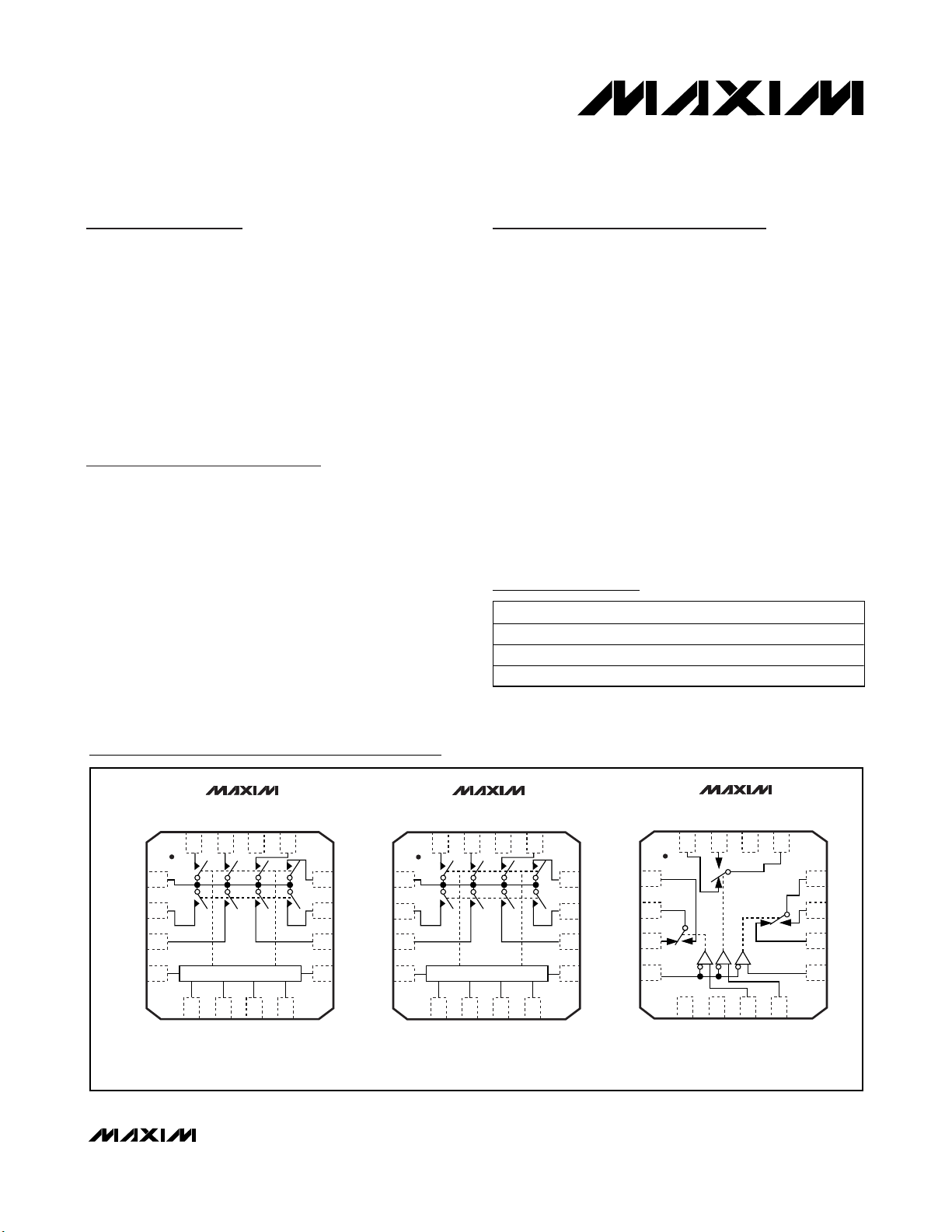
Pin Configurations/Functional Diagrams
Ordering Information
19-2941; Rev 1; 6/07
For pricing, delivery, and ordering information, please contact Maxim Direct at 1-888-629-4642,
or visit Maxim’s website at www.maxim-ic.com.
Ordering Information continued at end of data sheet.
*EP = Exposed pad.
PIN CONFIGURATIONS/FUNCTIONAL DIAGRAMS CONTINUED AT END OF DATA SHEET.
PART TEMP RANGE PIN-PACKAGE
MAX4581LESE -40°C to +85°C 16 Narrow SO
MAX4581LEEE -40°C to +85°C 16 QSOP
MAX4581LETE -40°C to +85°C 16 TQFN-EP* (4mm x 4mm)
TOP VIEW
MAX4581L
X6
X4
VCCX2
16
15 14 13
X1
12
11
10
9
Y
1
X0
Y3
2
X3
Y1
3
A
ENABLE
4
ENABLE
X
1
X7
2
X5
3
4
LOGIC
5678
B
GND
C
GND
THIN QFN THIN QFN THIN QFN
MAX4582L
Y2
Y0
VCCX2
16
15 14 13
LOGIC
5678
B
GND
GND
A
X1
12
X
11
X0
10
ENABLE
X3
9
MAX4583L
Y0
Y1
VCCY
16
15 14 13
Z1
1
Z
2
Z0
3
4
5678
B
GND
C
GND
X
12
X1
11
X0
10
A
9
Page 2
MAX4581L/MAX4582L/MAX4583L
Low-Voltage, CMOS Analog
Multiplexers/Switches
2 _______________________________________________________________________________________
ABSOLUTE MAXIMUM RATINGS
ELECTRICAL CHARACTERISTICS
(VCC= +12V ±5%, V_H= 2.0V, V_L= 0.8V, TA= T
MIN
to T
MAX
, unless otherwise noted. Typical values are at TA = +25°C.) (Notes 2, 3)
Stresses beyond those listed under “Absolute Maximum Ratings” may cause permanent damage to the device. These are stress ratings only, and functional
operation of the device at these or any other conditions beyond those indicated in the operational sections of the specifications is not implied. Exposure to
absolute maximum rating conditions for extended periods may affect device reliability.
Note 1: Voltages exceeding VCCor GND on any signal terminal are clamped by internal diodes. Limit forward-diode current to max-
imum current rating.
(All Voltages Referenced to GND, Unless Otherwise Noted.)
V
CC
.........................................................................-0.3V to +13V
Voltage At Any Pin (Note 1) ...........(GND - 0.3V) to (V
CC
+ 0.3V)
Continuous Current into Any Terminal ..............................±20mA
Peak Current X_, Y_ or Z_
(pulsed at 1ms, 10% duty cycle) ..................................±40mA
ESD per Method 3015.7 ..................................................>2000V
Continuous Power Dissipation (T
A
= +70°C)
16-Pin Narrow SO (derate 8.7mW/°C above +70°C) ...696mW
16-Pin QSOP (derate 8.3mW/°C above +70°C)...........667mW
16-Pin Thin QFN (derate 16.9mW/°C above +70°C) .1349mW
Operating Temperature Range ...........................-40°C to +85°C
Storage Temperature Range .............................-65°C to +150°C
Junction Temperature......................................................+150°C
Lead Temperature (soldering, 10s) .................................+300°C
)
(
)
PARAMETER SYMBOL CONDITIONS TEMP MIN
ANALOG SWITCH
Analog Signal Range VX, V
Switch On-Resistance R
Switch On-Resistance
Match Between Channels
Switch On-Resistance
Flatness
X_, Y_, Z_ Off-Leakage
X, Y, Z Off-Leakage
X, Y, Z On-Leakage
ΔR
R
FLAT(ON
I
X_(OFF)
I
Y_(OFF)
I
Z_(OFF)
I
X(OFF)
I
Y(OFF)
I
Z(OFF)
I
X(ON)
I
Y(ON)
I
Z(ON)
Y, VZ
ON
ON
VCC = 11.4V; IX, IY, IZ = 1mA;
V
X
VCC = 11.4V; IX, IY, IZ = 1mA;
V
X
VCC = 11.4V; IX, IY, IZ = 1mA;
V
X_
(Note 5)
,
VCC = 12.6V;
V
,
X_
V
X
VCC = 12.6V;
,
V
X_
,
1V, 10V;
V
X
1V
,
VCC = 12.6V;
,
V
X
1V (Note 6)
, V
Y, VZ
, V
Y, VZ
, V
Y_, VZ_
, VY_, VZ_ = 1V, 10V;
, VY, VZ = 10V, 1V (Note 6)
, VY_, VZ_ =
, VY, VZ = 10V,
Note 6
, VY, VZ = 10V,
= 10V
= 10V (Note 4)
= 1.5V, 6V, 10V
MAX4581L
MAX4582L/
MAX4583L
MAX4581L
MAX4582L/
MAX4583L
-40°C to +85°C 0 V
+25°C 50 80
-40°C to +85°C 100
+25°C 1 4
-40°C to +85°C 5
+25°C 5 12
-40°C to +85°C 15
+25°C -2 +2
-40°C to +85°C -10 +10
+25°C -2 +2
-40°C to +85°C -100 +100
+25°C -2 +2
-40°C to +85°C -50 +50
+25°C -2 +2
-40°C to +85°C -100 +100
+25°C -2 +2
-40°C to +85°C -50 +50
TYP
(NOTE 3)
MAX UNITS
CC
V
Ω
Ω
Ω
nA
nA
nA
Page 3
MAX4581L/MAX4582L/MAX4583L
Low-Voltage, CMOS Analog
Multiplexers/Switches
_______________________________________________________________________________________ 3
ELECTRICAL CHARACTERISTICS (continued)
(VCC= +12V ±5%, V_H= 2.0V, V_L= 0.8V, TA= T
MIN
to T
MAX
, unless otherwise noted. Typical values are at TA = +25°C.) (Notes 2, 3)
)
PARAMETER SYMBOL CONDITIONS TEMP MIN
DIGITAL I/O (INH, ADD_)
, VBH,
V
Logic Input High
Threshold
Logic Input Low
Threshold
Input Current High
Input Current Low
AH
V
CH
V
ENABLE_H
V
, VBL,
AL
V
CL
V
ENABLE_L
I
AH, IBH
I
CH
I
ENABLE_H
I
AL, IBL
I
CL
I
ENABLE_L
,
,
,
,
,
,
VA, VB, VC, V
VA, VB, VC, V
SWITCH DYNAMIC CHARACTERISTICS
VX_, VY_, VZ_ = 10V,
Enable Turn-On Time t
ON
R
= 300Ω,
L
= 35pF, Figure 1
C
L
VX_, VY_, VZ_ = 10V,
Enable Turn-Off Time t
OFF
R
= 300Ω,
L
= 35pF, Figure 1
C
L
VX_, VY_, VZ_ = 10V,
Address Transition Time t
TRANS
= 300Ω,
R
L
C
= 35pF, Figure 2
L
VX_, VY_, VZ_ = 10V,
Break-Before-Make Time t
BBM
Charge Injection (Note 7) Q
C
X_(OFF)
Input Off-Capacitance
C
Y_(OFF)
C
Z_(OFF
R
= 300Ω,
L
= 35pF, Figure 3
C
L
C
= 1nF, RS = 0Ω, VS = 0V,
L
Figure 4
,
VX_, VY_, VZ_ = 0V,
,
ƒ = 1MHz, Figure 5
-40°C to +85°C 1.5 2.0 V
-40°C to +85°C 0.8 1.5 V
= 2.0V +25°C -1 +1 µA
ENABLE
= 0.8V +25°C -1 +1 µA
ENABLE
+25°C 100 200
-40°C to +85°C 200
+25°C 40 100
-40°C to +85°C 150
+25°C 90 200
-40°C to +85°C 200
-40°C to +85°C 20 ns
+25°C 0.5 pC
+25°C 4 pF
TYP
(NOTE 3)
MAX UNITS
ns
ns
ns
Output Off-Capacitance
C
X(OFF)
C
Y(OFF)
C
Z(OFF)
C
X(OFF)
C
Y(OFF)
C
Z(OFF)
,
,
,
,
VX_, VY_,
= 0V,
V
Z_
ƒ = 1MHz,
Figure 5
VX_, VY_,
V
= 0V,
Z_
ƒ = 1MHz,
Figure 5
MAX4581L 18
MAX4582L 10
+25°C
MAX4583L
MAX4581L 25
MAX4582L 17Output On-Capacitance
MAX4583L
+25°C
12.5
pF
6
pF
Page 4
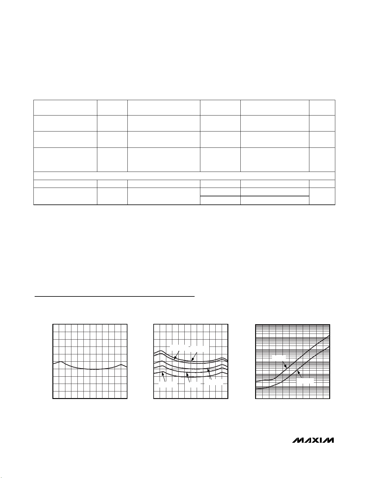
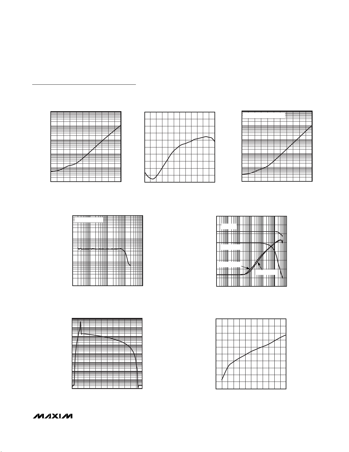
100
90
70
60
80
0
0678910
11
12345
12
ON-RESISTANCE vs. V
COM
MAX4581L/2L/3L toc01
V
COM
(V)
ON-RESISTANCE (Ω)
50
40
30
20
10
100
90
70
60
80
0
0678910
11
12345
12
ON-RESISTANCE vs. V
COM
MAX4581L/2L/3L toc02
V
COM
(V)
ON-RESISTANCE (Ω)
50
40
30
20
10
TA = +70°C
TA = +85°C
TA = -40°C
TA = +25°C
TA = 0°C
100
10
1
0.0001
-40 35 50 65 80 95 110-25 -10 5 20 125
OFF-LEAKAGE CURRENT
vs. TEMPERATURE
MAX4581L/2L/3L toc03
TEMPERATURE (°C)
OFF-LEAKAGE CURRENT (nA)
0.1
0.01
0.001
IX, IY, I
Z
IX_, IY_, I
Z_
Typical Operating Characteristics
(VCC= 12V, VEN= GND, TA= +25°C, unless otherwise noted.)
MAX4581L/MAX4582L/MAX4583L
Low-Voltage, CMOS Analog
Multiplexers/Switches
4 _______________________________________________________________________________________
ELECTRICAL CHARACTERISTICS (continued)
(VCC= +12V ±5%, V_H= 2.0V, V_L= 0.8V, TA= T
MIN
to T
MAX
, unless otherwise noted. Typical values are at TA = +25°C.) (Notes 2, 3)
Note 2: Thin QFN packages are production tested at TA= +85°C. Limits over temperature are guaranteed by design.
Note 3: The algebraic convention used in this data sheet is where the most negative value is the minimum column.
Note 4: ΔR
ON
= R
ON(MAX)
- R
ON(MIN)
.
Note 5: Flatness is defined as the difference between the maximum and minimum value of on-resistance as measured over the
specified analog signal ranges.
Note 6: Leakage parameters are 100% tested at the maximum-rated hot operating temperature and guaranteed by design at T
A
=
+25°C.
Note 7: Guaranteed by design, not production tested.
PARAMETER SYMBOL CONDITIONS TEMP MIN
Off-Isolation V
Channel-to-Channel
Crosstalk
V
ISO
CT
Total Harmonic Distortion THD
RL = 50Ω, ƒ = 1MHz
(Figure 7)
RL = 50Ω, ƒ = 1MHz
(Figure 7)
R
L
V
X_
ƒ = 20Hz to 20kHz
POWER SUPPLY
Power-Supply Range V
Power-Supply Current I
CC
CC
VCC = 12.6V; VA, VB, VZ,
V
ENABLE
= 600Ω,
or VY_ or VZ_ = 5V
= VCC or 0V
P-P
TYP
(NOTE 3)
+25°C -90 dB
+25°C -96 dB
,
+25°C 0.02 %
2 12.6 V
+25°C -1 +1
-40°C to +85°C -10 +10
MAX UNITS
µA
Page 5
MAX4581L/MAX4582L/MAX4583L
Low-Voltage, CMOS Analog
Multiplexers/Switches
_______________________________________________________________________________________ 5
Typical Operating Characteristics (continued)
(VCC= 12V, VEN= GND, TA= +25°C, unless otherwise noted.)
ON-LEAKAGE CURRENT
100
10
1
0.1
ON-LEAKAGE CURRENT (nA)
0.01
0.001
-40 35 50 65 80 95 110-25 -10 5 20 125
TEMPERATURE (°C)
TOTAL HARMONIC DISTORTION
vs. FREQUENCY
0.1
600Ω IN AND OUT
0.01
0.001
TOTAL HARMONIC DISTORTION (%)
0.0001
10 1k 10k100 100k
FREQUENCY (Hz)
vs. TEMPERATURE
MAX4581L/2L/3L toc04
CHARGE INJECTION (pC)
CHARGE INJECTION vs. V
10
9
8
7
6
5
4
3
2
1
0
023451678
MAX4581L/2L/3L toc07
V
COM
SUPPLY CURRENT
COM
9
10 11 12
(V)
1000
100
MAX4581L/2L/3L toc05
10
SUPPLY CURRENT (nA)
0.1
0.01
1
-40 35 50 65 80 95 110-25 -10 5 20 125
FREQUENCY RESPONSE
30
10
ON-LOSS
-10
-30
ON-PHASE
-50
GAIN (dB)
-70
OFF-ISOLATION
-90
-110
-130
0.001 1 10 1000.01 0.1 1000
FREQUENCY (MHz)
vs. TEMPERATURE
V
, VA, VB, VC = 0V OR V
INH
TEMPERATURE (°C)
CROSSTALK
MAX4581L/2L/3L toc08
CC
MAX4581L/2L/3L toc06
90
60
30
0
-30
-60
PHASE (DEGREES)
-90
-120
-150
SUPPLY CURRENT
vs. LOGIC-LEVEL VOLTAGE
10,000
1000
100
10
1
0.1
SUPPLY CURRENT (μA)
0.01
0.001
0.0001
06
2
1
45
3
LOGIC-LEVEL VOLTAGE (V)
789
10 11
MAX4581L/2L/3L toc09
12
2.0
1.8
1.6
1.4
1.2
1.0
0.8
0.6
LOGIC-LEVEL THRESHOLD (V)
0.4
0.2
0
LOGIC-LEVEL THRESHOLD
vs. SUPPLY VOLTAGE
0 2341576 8 9 101112
SUPPLY VOLTAGE (V)
MAX4581L/2L/3L toc10
Page 6

MAX4581L/MAX4582L/MAX4583L
Low-Voltage, CMOS Analog
Multiplexers/Switches
6 _______________________________________________________________________________________
Pin Description
Note: Input and output pins are identical and interchangeable. Any may be considered an input or output; signals pass equally well
in both directions.
PIN
MAX4581L MAX4582L MAX4583L NAME FUNCTION
SO/QSOP QFN SO/QSOP QFN SO/QSOP QFN
1, 2, 4, 5,
12–15
3 1 13 11 14 12 X Analog Switch X Output
6 4 6 4 6 4 Enable
7, 8 5, 6 7, 8 5, 6 7, 8 5, 6 GND
9 7 — — 9 7 C Digital Address C Input
10 8 9 7 10 8 B Digital Address B Input
11 9 10 8 11 9 A Digital Address A Input
16 14 16 14 16 14 V
——
— — 1, 2, 4, 5
— — 3 1 15 13 Y Analog Switch Y Output
— — — — 13 11 X1 Analog Switch X Normally Open Input
— — — — 12 10 X0 Analog Switch X Normally Closed Input
— — — — 1 15 Y1 Analog Switch Y Normally Open Input
— — — — 2 16 Y0 Analog Switch Y Normally Closed Input
— — — — 3 1 Z1 Analog Switch Z Normally Open Input
— — — — 5 3 Z0 Analog Switch Z Normally Closed Input
— — — — 4 2 Z Analog Switch Z Output
— EP — EP — EP
2, 3,
10–13,
15, 16
— — — — X0–X7 Analog Switch Inputs 0–7
CC
11, 12,
14, 15,
9, 10,
12, 13
2, 3,
15, 16
— — X0–X3 Analog Switch X Inputs 0–3
— — Y0–Y3 Analog Switch Y Inputs 0–3
Exposed
Pad
Digital Enable Input. Drive enable low or
connect to GND for normal operation.
Ground. Connect to digital ground. (Analog
signals have no ground reference; they are
limited to V
Positive Analog and Digital Supply Voltage
Input. Bypass with a 0.1µF capacitor to GND.
Bottom of QFN package only. Contains an
exposed pad that must be connected
externally to V
CC.
)
CC
.
Page 7

MAX4581L/MAX4582L/MAX4583L
Low-Voltage, CMOS Analog
Multiplexers/Switches
_______________________________________________________________________________________ 7
Detailed Description
The MAX4581L/MAX4582L/MAX4583L are low-voltage,
CMOS analog ICs that operate from a single supply of
+2V to +12V. The MAX4581L is configured as an 8channel multiplexer, the MAX4582L as two 4-channel
multiplexers, and the MAX4583L as three singlepole/double-throw (SPDT) switches. These devices can
handle rail-to-rail analog signals with only 2nA of offleakage current at +25°C.
The MAX4581L/MAX4582L/MAX4583L are TTL/CMOSlogic compatible with 0.8V to 2.0V logic thresholds for
all digital inputs when operating from a +12V supply.
Applications Information
Power-Supply Considerations
The MAX4581L/MAX4582L/MAX4583Ls’ construction is
typical of most CMOS analog switches. The supply
input, VCC, is used to power the internal CMOS switches and sets the limit of the analog voltage on any
switch. Reverse ESD protection diodes are internally
connected between each analog signal pin and both
VCCand GND. If any analog signal exceeds VCCor
goes below GND, one of these diodes conducts.
During normal operation, these reverse-biased ESD
diodes leak, causing the only current drawn from V
CC
or GND. Virtually all the analog leakage current comes
from the ESD diodes. Although the ESD diodes on a
given signal pin are identical, and therefore fairly well
balanced, they are reverse biased differently by either
V
CC
or GND and the analog signal. This means that
leakage varies as the analog signal varies. The difference in the two diodes’ leakage to VCCand GND constitutes the analog signal-path leakage current.
Because there is no connection between the analog
signal paths and GND, all analog leakage current flows
between each pin and one of the supply terminals, not
to the other switch terminal. Because of this, both sides
of a given switch can show leakage currents of either
the same or opposite polarity.
VCCand GND power the internal logic and logic-level
translators, and set both the input and output logic limits. The logic-level translators convert the logic levels
into switched VCCand GND signals to drive the gates
of the analog switches. This drive signal is the only
connection between the logic supplies (and signals)
and the analog supplies. The logic-level thresholds are
TTL/CMOS compatible when VCCis +12V.
Overvoltage Protection
Proper power-supply sequencing is recommended for
all CMOS devices. Do not exceed the absolute maximum ratings because stresses beyond the listed ratings can cause permanent damage to the devices.
Always sequence VCCfirst, followed by the logic inputs
and analog signals.
Pin Nomenclature
The MAX4581L/MAX4582L/MAX4583L are pin compatible with the industry-standard 74HC4051/74HC4052/
74HC4053 and the MAX4051/MAX4052/MAX4053.
Table 1. Truth Table/Switch Programming
X = Don’t care.
*C not present on MAX4582L.
Note: Input and output pins are identical and interchangeable. Either may be considered an input or output; signals pass equally
well in either direction.
ENABLE
INPUT
H X X X All switches open All switches open All switches open
L L L L X–X0 X–X0, Y–Y0 X–X0, Y–Y0, Z–Z0
L L L H X–X1 X–X1, Y–Y1 X–X1, Y–Y0, Z–Z0
L L H L X–X2 X–X2, Y–Y2 X–X0, Y–Y1, Z–Z0
L L H H X–X3 X–X3, Y–Y3 X–X1, Y–Y1, Z–Z0
L H L L X–X4 X–X0, Y–Y0 X–X0, Y–Y0, Z–Z1
L H L H X–X5 X–X1, Y–Y1 X–X1, Y–Y0, Z–Z1
L H H L X–X6 X–X2, Y–Y2 X–X0, Y–Y1, Z–Z1
L H H H X–X7 X–X3, Y-Y3 X–X1, Y–Y1, Z–Z1
SELECT INPUTS ON SWITCHES
C* B A MAX4581L MAX4582L MAX4583L
Page 8

MAX4581L/MAX4582L/MAX4583L
Low-Voltage, CMOS Analog
Multiplexers/Switches
8 _______________________________________________________________________________________
Test Circuits/Timing Diagrams
Figure 1. Enable Switching Times
V
CC
V
CC
X1–X7
CC
CC
X0–Y0
X1–X3, Y1–Y3
X, Y
X0
V
CC
V
35pF
35pF
OUT
V
OUT
X
300
Ω
V
CC
300
Ω
V
ENABLE
V
ENABLE
A
B
C
MAX4581L
ENABLE
50
Ω
GND
V
A
B
V
MAX4582L
ENABLE
50
Ω
GND
V
CC
V
ENABLE
V
ENABLE
0V
V
X0
V
OUT
0V
t
ON
V
CC
0V
V
,
X0
V
Y0
V
OUT
0V
t
ON
50%
50%
90%
90%
90%
90%
t
OFF
t
OFF
V
A
B
C
CC
V
CC
X0, Y0, Z0
X1, Y1, Z1
V
CC
MAX4583L
V
ENABLE
ENABLE
50
Ω
GND
X, Y, Z
300
Ω
35pF
V
OUT
V
ENABLE
V
V
V
V
V
OUT
VX1,
V
V
CC
50%
0V
,
X0
,
Y0
Z0
,
Y1
Z1
t
ON
90%
90%
t
OFF
Page 9

MAX4581L/MAX4582L/MAX4583L
Low-Voltage, CMOS Analog
Multiplexers/Switches
_______________________________________________________________________________________ 9
VA, VB, V
Figure 2. Address Transition Time
V
CC
C
50
Ω
A
B
C
V
CC
MAX4581L
X1–X6
X0
V
CC
X7
V
, VB, V
A
V
CC
C
50%
0V
V
X0
90%
VA, V
B
50
VA, V
50%
50%
90%
90%
90%
90%
90%
t
TRANS
t
TRANS
t
TRANS
V
35pF
35pF
35pF
OUT
V
X7
t
TRANS
V
CC
V
, V
A
B
0V
V
,
X0
V
Y0
V
OUT
V
OUT
V
, VB, V
A
VX3,
V
V
Y3
t
TRANS
CC
C
0V
V
,
X0
,
V
Y0
V
Z0
V
OUT
V
OUT
VX1,
V
,
Y1
V
Z1
t
TRANS
ENABLE
GND
V
CC
V
A
Ω
B
CC
X1, X2, Y1, Y2
MAX4582L
ENABLE
GND
V
CC
B
50
Ω
A, B, C
V
CC
X0, Y0
X3, Y3
X, Y
X1, Y1, Z1
X0, Y0, Z0
X
300
Ω
V
CC
300
Ω
V
CC
MAX4583L
ENABLE
GND
X, Y, Z
300
Ω
V
CC
Page 10

MAX4581L/MAX4582L/MAX4583L
Low-Voltage, CMOS Analog
Multiplexers/Switches
10 ______________________________________________________________________________________
Figure 3. Break-Before-Make Interval
Figure 4. Charge Injection
VA, VB, V
50
VA, VB, V
A
B
ENABLE
V
CC
V
CC
MAX4582L
GND
50%
t
BBM
X0–X3,
Y0–Y3
X, Y
80%
tR < 20ns
< 20ns
t
F
V
CC
V
OUT
300
35pF
Ω
V
CC
C
Ω
A
B
C
V
CC
X0–X7
V
CC
VA, V
B
50
Ω
MAX4581L
V
35pF
OUT
VA, VB, V
, VY, V
V
X
V
CC
C
0V
Z
ENABLE
GND
V
CC
C
50
Ω
A, B, C
V
CC
X0, X1, Y0,
Y1, Z0, Z1
X
300
Ω
V
CC
MAX4583L
V
ENABLE
GND
X, Y, Z
300
V
OUT
35pF
Ω
OUT
0V
V
CC
V
CC
X_, Y_, Z_
V
ENABLE
V
CC
0V
CHANNEL
SELECT
A
B
C
MAX4581L
MAX4582L
V
V
ENABLE
50Ω
ENABLE
MAX4583L
GND
X, Y, Z
C
= 1000pF
L
V
OUT
OUT
ΔV
IS THE MEASURED VOLTAGE DUE TO CHARGE-
OUT
TRANSFER ERROR Q WHEN THE CHANNEL TURNS OFF.
Q = ΔV
X CL.
OUT
ΔV
OUT
Page 11

MAX4581L/MAX4582L/MAX4583L
Low-Voltage, CMOS Analog
Multiplexers/Switches
______________________________________________________________________________________ 11
CHANNEL
Figure 5. NO/COM Capacitance
Figure 6. Off-Isolation, On-Loss, and Crosstalk
SELECT
A
B
C
ENABLE
V
CC
V
CC
X_, Y_, Z_
MAX4581L
MAX4582L
MAX4583L
GND
1MHz
X, Y, Z
CAPACITANCE
ANALYZER
V
CC
V
CC
CHANNEL
SELECT
A
B
C
MAX4581L
MAX4582L
MAX4583L
ENABLE
GND
MEASUREMENTS ARE STANDARDIZED AGAINST SHORT AT SOCKET TERMINALS.
OFF-ISOLATION IS MEASURED BETWEEN COM AND "OFF" NO TERMINAL ON EACH SWITCH.
ON-LOSS IS MEASURED BETWEEN COM AND "ON" NO TERMINAL ON EACH SWITCH.
CROSSTALK (MAX4582/MAX4583) IS MEASURED FROM ONE CHANNEL (A, B, C) TO ALL OTHER CHANNELS.
SIGNAL DIRECTION THROUGH SWITCH IS REVERSED; WORST VALUES ARE RECORDED.
X_, Y_, Z_
X, Y, Z
NETWORK
ANALYZER
V
IN
V
OUT
50Ω 50Ω
MEAS.
50Ω 50Ω
REF.
OFF-ISOLATION = 20log x
ON-LOSS = 20log x
CROSSTALK = 20log x
V
OUT
V
IN
V
OUT
V
IN
V
OUT
V
IN
Page 12

MAX4581L/MAX4582L/MAX4583L
Low-Voltage, CMOS Analog
Multiplexers/Switches
12 ______________________________________________________________________________________
Ordering Information (continued)
Pin Configurations/Functional Diagrams (continued)
Chip Information
TRANSISTOR COUNT: 219
PROCESS: CMOS
*EP = Exposed pad.
____________________Revision History
Pages changed at Rev 1: 1, 6, 12, 16
TOP VIEW
ENABLE
GND
GND
MAX4581L
X4
1
X6
2
X
3
X7
4
X5
5
6
7
8
LOGIC
V
16
CC
X2
15
X1
14
X0
13
X3
12
11
A
10
B
9
C
Y0
Y2
Y
Y3
Y1
ENABLE
GND
GND
SO/QSOP
1
2
3
4
5
6
7
8
MAX4582L
LOGIC
SO/QSOP
V
16
CC
X2
15
X1
14
X
13
X0
12
11
X3
10
A
9
B
PART TEMP RANGE PIN-PACKAGE
MAX4582LESE -40°C to +85°C 16 Narrow SO
MAX4582LEEE -40°C to +85°C 16 QSOP
MAX4582LETE -40°C to +85°C 16 TQFN-EP* (4mm x 4mm)
MAX4583LESE -40°C to +85°C 16 Narrow SO
MAX4583LEEE -40°C to +85°C 16 QSOP
MAX4583LETE -40°C to +85°C 16 TQFN-EP* (4mm x 4mm)
MAX4583L
Y1
1
Y0
2
Z1
3
Z
4
Z0
5
ENABLE
6
GND
7
GND
8
SO/QSOP
V
16
CC
Y
15
X
14
X1
13
X0
12
11
A
10
B
9
C
Page 13

MAX4581L/MAX4582L/MAX4583L
Low-Voltage, CMOS Analog
Multiplexers/Switches
______________________________________________________________________________________ 13
Package Information
(The package drawing(s) in this data sheet may not reflect the most current specifications. For the latest package outline information
go to www.maxim-ic.com/packages
.)
N
1
TOP VIEW
D
e
FRONT VIEW
INCHES
DIM
MIN
0.053A
0.004
A1
0.014
B
0.007
C
e 0.050 BSC 1.27 BSC
0.150
HE
A
B
A1
C
L
E
H 0.2440.228 5.80 6.20
0.016L
VARIATIONS:
INCHES
MINDIM
D
0.189 0.197 AA5.004.80 8
0.337 0.344 AB8.758.55 14
D
0∞-8∞
SIDE VIEW
MAX
0.069
0.010
0.019
0.010
0.157
0.050
MAX
0.3940.386D
MILLIMETERS
MAX
MIN
1.35
1.75
0.10
0.25
0.35
0.49
0.19
0.25
3.80 4.00
0.40 1.27
MILLIMETERS
MAX
MIN
9.80 10.00
N MS012
16
AC
SOICN .EPS
PROPRIETARY INFORMATION
TITLE:
PACKAGE OUTLINE, .150" SOIC
REV.DOCUMENT CONTROL NO.APPROVAL
21-0041
1
B
1
Page 14

MAX4581L/MAX4582L/MAX4583L
Low-Voltage, CMOS Analog
Multiplexers/Switches
14 ______________________________________________________________________________________
Package Information (continued)
(The package drawing(s) in this data sheet may not reflect the most current specifications. For the latest package outline information
go to www.maxim-ic.com/packages
.)
QSOP.EPS
PACKAGE OUTLINE, QSOP .150", .025" LEAD PITCH
21-0055
1
F
1
Page 15

MAX4581L/MAX4582L/MAX4583L
Low-Voltage, CMOS Analog
Multiplexers/Switches
______________________________________________________________________________________ 15
Package Information (continued)
(The package drawing(s) in this data sheet may not reflect the most current specifications. For the latest package outline information
go to www.maxim-ic.com/packages
.)
24L QFN THIN.EPS
PACKAGE OUTLINE,
12, 16, 20, 24, 28L THIN QFN, 4x4x0.8mm
21-0139
1
F
2
Page 16

MAX4581L/MAX4582L/MAX4583L
Low-Voltage, CMOS Analog
Multiplexers/Switches
Maxim cannot assume responsibility for use of any circuitry other than circuitry entirely embodied in a Maxim product. No circuit patent licenses are
implied. Maxim reserves the right to change the circuitry and specifications without notice at any time.
16 ____________________Maxim Integrated Products, 120 San Gabriel Drive, Sunnyvale, CA 94086 408-737-7600
© 2007 Maxim Integrated Products is a registered trademark of Maxim Integrated Products.
Package Information (continued)
(The package drawing(s) in this data sheet may not reflect the most current specifications. For the latest package outline information
go to www.maxim-ic.com/packages
.)
PACKAGE OUTLINE,
12, 16, 20, 24, 28L THIN QFN, 4x4x0.8mm
21-0139
F
2
2
 Loading...