

For pricing delivery, and ordering information please contact Maxim Direct! at 1-888-629-4642,
or visit Maxim’s website at www.maxim-ic.com.
________________General Description
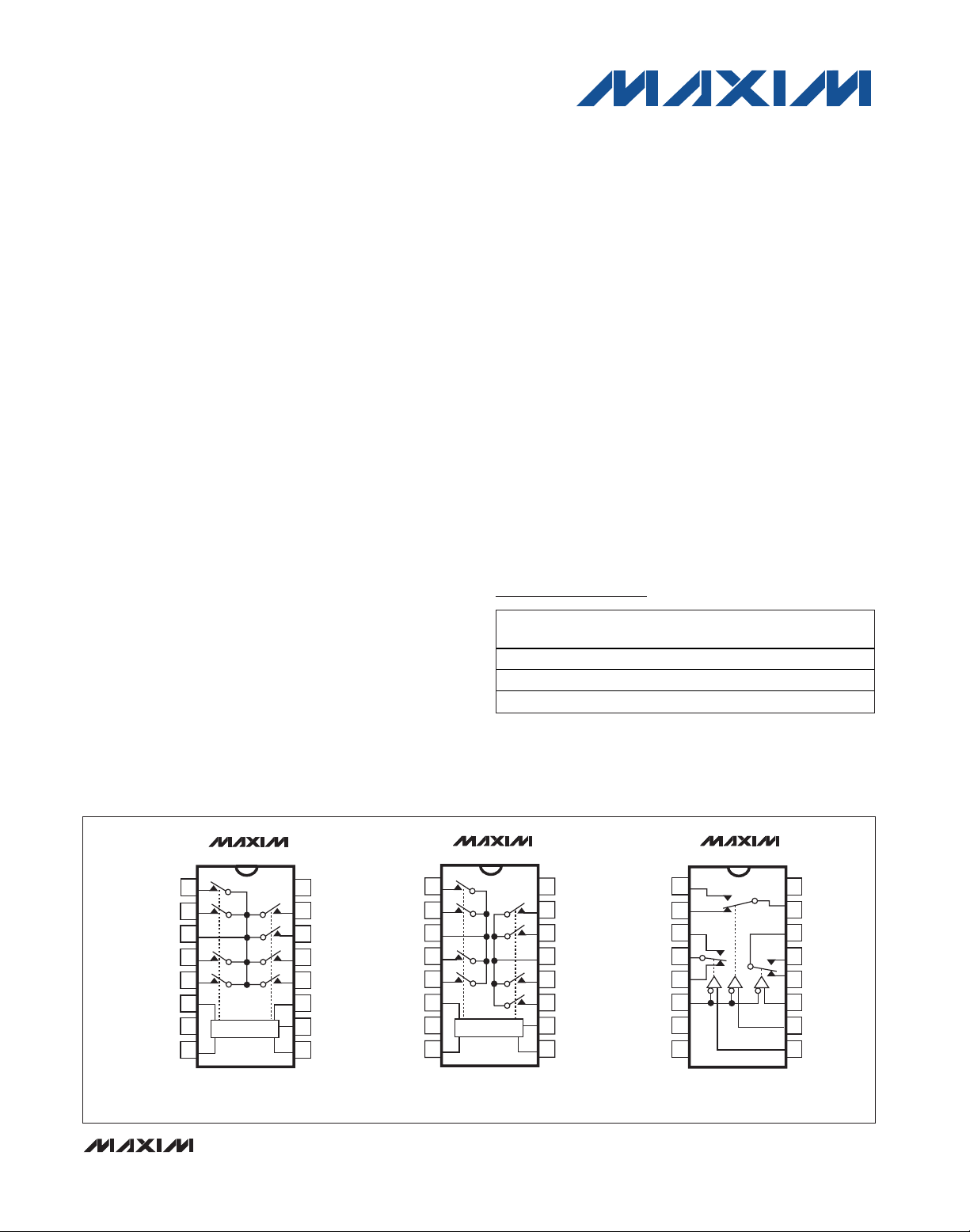
The MAX4581/MAX4582/MAX4583 are low-voltage,
CMOS analog ICs configured as an 8-channel multiplexer
(MAX4581), two 4-channel multiplexers (MAX4582), and
three single-pole/double-throw (SPDT) switches
(MAX4583).
These CMOS devices can operate continuously with
±2V to ±6V dual power supplies or a +2V to +12V single supply. Each switch can handle rail-to-rail analog
signals. The off-leakage current is only 1nA at +25°C or
5nA at +85°C.
All digital inputs have 0.8V to 2.4V logic thresholds,
ensuring TTL/CMOS-logic compatibility when using a
single +5V or dual ±5V supplies.
________________________Applications
Battery-Operated Equipment
Audio and Video Signal Routing
Low-Voltage Data-Acquisition Systems
Communications Circuits
Automotive
____________________________Features
o MAX4582 Available in AEC-Q100 Qualified
Version
o Offered in Automotive Temperature Range
(-40°C to +125°C)
o Guaranteed On-Resistance
80Ω with ±5V Supplies
150ΩΩwith Single +5V Supply
o Guaranteed On-Resistance Match Between
Channels
o Guaranteed Low Off-Leakage Current
1nA at +25°C
o Guaranteed Low On-Leakage Current
1nA at +25°C
o +2V to +12V Single-Supply Operation
±2V to ±6V Dual-Supply Operation
o TTL/CMOS-Logic Compatible
o Low Distortion: < 0.02% (600Ω)
o Low Crosstalk: < -96dB (50Ω, MAX4582)
o High Off-Isolation: < -74dB (50Ω)
MAX4581/MAX4582/MAX4583
Low-Voltage, CMOS Analog
Multiplexers/Switches
________________________________________________________________
Maxim Integrated Products
1
____________________________________Pin Configurations/Functional Diagrams
19-1328; Rev 6; 3/12
Ordering Information continued at end of data sheet.
Ordering Information
Pin Configurations continued at end of data sheet.
+
Denotes a lead(Pb)-free/RoHS-compliant package.
PART TEMP RANGE
PINPACKAGE
MAX4581CPE+ 0°C to +70°C 16 PDIP —
MAX4581CSE+ 0°C to +70°C 16 Narrow SO —
MAX4581CUE+ 0°C to +70°C 16 TSSOP —
TOP
MARK
TOP VIEW
MAX4581
++
X4
1
X6
2
X
3
X7
4
X5
5
ENABLE
6
V
GND
7
EE
8
LOGIC
PDIP/SO/QSOP/TSSOP
ENABLE
V
GND
Y0
Y2
Y
Y3
Y1
EE
V
16
CC
X2
15
X1
14
X0
13
X3
12
11
A
10
B
9
C
MAX4582
1
2
3
4
5
6
7
8
LOGIC
16
15
14
13
12
11
10
9
PDIP/SO/QSOP/TSSOP
ENABLE
V
GND
Y1
Y0
Z1
Z
Z0
EE
V
CC
X2
X1
X
X0
X3
A
B
PDIP/SO/QSOP/TSSOP
MAX4583
+
1
2
3
4
5
6
7
8
V
16
CC
Y
15
X
14
X1
13
X0
12
11
A
10
B
9
C
MAX4581/MAX4582/MAX4583
Low-Voltage, CMOS Analog
Multiplexers/Switches
2 _______________________________________________________________________________________
ABSOLUTE MAXIMUM RATINGS
ELECTRICAL CHARACTERISTICS—Dual Supplies
(VCC= 4.5V to 5.5V, VEE= -4.5V to -5.5V, V_H= 2.4V, V_L= 0.8V, TA= T
MIN
to T
MAX
, unless otherwise noted. Typical values are at
T
A
= +25°C.)
Stresses beyond those listed under “Absolute Maximum Ratings” may cause permanent damage to the device. These are stress ratings only, and functional
operation of the device at these or any other conditions beyond those indicated in the operational sections of the specifications is not implied. Exposure to
absolute maximum rating conditions for extended periods may affect device reliability.
Voltages Referenced to V
EE
VCC.........................................................................-0.3V to 13V
Voltage into Any Terminal (Note 1) ...(V
EE
- 0.3V) to (VCC+ 0.3V)
Continuous Current into Any Terminal..............................±20mA
Peak Current, X_, Y_, Z_
(pulsed at 1ms, 10% duty cycle) ...................................±40mA
ESD per Method 3015.7 ..................................................>2000V
Continuous Power Dissipation (T
A
= +70°C)
16-Pin PDIP (derate 10.53mW/°C above +70°C).............842mW
16-Pin Narrow SO (derate 8.70mW/°C above +70°C) .....696mW
16-Pin QSOP (derate 8.3mW/°C above +70°C)...............667mW
16-Pin TSSOP (derate 9.4mW/°C above +70°C) .............755mW
16-Pin TQFN (derate 14.7mW/°C above +70°C) ...........1177mW
Operating Temperature Ranges
MAX458_C_ .........................................................0°C to +70°C
MAX458_E_ ......................................................-40°C to +85°C
MAX458_A_.....................................................-40°C to +125°C
Storage Temperature Range .............................-65°C to +150°C
Lead Temperature (soldering, 10s) .................................+300°C
Soldering Temperature (reflow) .......................................+260°C
+25°C
VC, E, AVX, VY, V
Z
Analog-Signal Range
Ω
C, E, A
R
ON
Switch On-Resistance
VCC= 4.5V; VEE= -4.5V;
IX, IY, IZ = 1mA; VX, VY, VZ= 3.5V
VCC= 4.5V; VEE= -4.5V;
IX, IY, IZ= 1mA; VX, VY, VZ= 3.5V
+25°C
Ω
C, E, A
∆R
ON
Switch On-Resistance
Match Between
Channels (Note 3)
VCC= 5.5V; VEE= -5.5V;
V
X_
, VY_, VZ_= ±4.5V;
VX, VY, VZ= 4.5V
MAX4581
nA
I
X(OFF)
,
I
Y(OFF)
,
I
Z(OFF)
X, Y, Z Off-Leakage
(Note 5)
MAX4582
MAX4583
+25°C
VCC= 5V; VEE= -5V; IX, IY, IZ= 1mA;
VX, VY, VZ= 3V, 0V, -3V
Ω
+25°C
R
FLAT(ON)
Switch On-Resistance
Flatness (Note 4)
+25°C
Note 1: Voltages exceeding VCCor VEEon any signal terminal are clamped by internal diodes. Limit forward-diode current to maxi-
mum current rating.
14
6
50 80
V
EE
V
CC
-1 +1
100
410
-2 +2
C, E, A -10 +10
-1 +1
VCC= 5.5V; V
EE
= -5.5V;
VX_, VY_, VZ_= ±4.5V; VX, VY, VZ= 4.5V
nA
+25°C
I
X_(OFF)
,
I
Y_(OFF)
,
I
Z_(OFF)
X_, Y_, Z_ Off-Leakage
(Note 5)
CONDITIONS
MIN TYP MAX
(Note 2)
UNITSTEMPSYMBOLPARAMETER
C, E, A -100 +100
C, E, A -50 +50
C, E, A
-1 +1
-2 +2
C, E, A -100 +100
-50 +50
VCC= 5.5V; VEE= -5.5V;
VX, VY, VZ= ±4.5V
MAX4581
nA
I
X(ON)
,
I
Y(ON)
,
I
Z(ON)
X, Y, Z On-Leakage
(Note 5)
MAX4582
MAX4583
+25°C
+25°C
C, E, A 12
±
±
C, E, A 1.5 2.4 V
VAH, VBH,
V
CH
Logic Input Logic
Threshold High
V
VAL, VBL,
V
CL
C, E, A 0.8 1.5
Logic Input Logic
Threshold Low
ANALOG SWITCH
DIGITAL I/O
MAX4581/MAX4582/MAX4583
Low-Voltage, CMOS Analog
Multiplexers/Switches
_______________________________________________________________________________________ 3
ELECTRICAL CHARACTERISTICS—Dual Supplies (continued)
(VCC= 4.5V to 5.5V, VEE= -4.5V to -5.5V, V_H= 2.4V, V_L= 0.8V, TA= T
MIN
to T
MAX
, unless otherwise noted. Typical values are at
T
A
= +25°C.)
C, E, A 200
TA= +25°C
Address Transition Time t
TRANS
ns
VX_, VY_, VZ_= ±3V; RL= 300Ω; CL= 35pF;
Figure 2
90 200
C, E, A 150
TA= +25°C
Inhibit Turn-Off Time t
(OFF)
ns
VX_, VY_, VZ_= 3V; RL= 300Ω; CL= 35pF;
Figure 3
40 100
C, E, A -10 +10
C, E, A
TA= +25°C
200
TA= +25°C
Inhibit Turn-On Time t
(ON)
ns
VX_, VY_, VZ_= 3V; RL= 300Ω; CL= 35pF;
Figure 3
100 200
Power-Supply Current ICC, I
EE
µA
VCC= 5.5V, VEE= -5.5V,
VA, VB, VC, V
Enable
= V+ or 0V
-1 +1
PARAMETER SYMBOL TEMP UNITS
MIN TYP MAX
(Note 2)
CONDITIONS
TA= +25°CBreak-Before-Make Time
t
BBM
ns
VX_, VY_, VZ_= 3V; RL= 300Ω; CL= 35pF;
Figure 4
420
Charge Injection (Note 6)
Q pC
TA= +25°C
C = 1nF, RS = 0Ω, VS= 0V 0.5 5
pF
Output Off-Capacitance
C
X(OFF)
,
C
Y(OFF)
,
C
Z(OFF)
TA= +25°C
VX_, VY_, V
Z_
= 0V; f = 1MHz;
Figure 7
18
pF
Output On-Capacitance
C
X(ON)
,
C
Y(ON)
,
C
Z(ON)
TA= +25°C
VX_, VY_, V
Z_
= 0V; f = 1MHz;
Figure 7
25
MAX4581
MAX4581
dB
Off-Isolation
V
ISO
TA= +25°C
-74
10MAX4582
6MAX4583
17
12.5MAX4583
MAX4582
pF
Channel-to-Channel
Crosstalk
V
CT
TA= +25°C
RL= 50Ω, f = 1MHz, Figure 6
-96
MAX4582
dB
TA= +25°C
-78MAX4581
TA= +25°C
MAX4583
RL= 50Ω, f = 1MHz, Figure 6
%
Total Harmonic
Distortion
THD
TA= +25°C
RL= 600Ω, 5Vp-p, f = 20Hz to 20kHz
0.02
-73
VPower-Supply Range VCC, V
EE
C, E, A ±2 ±6
C, E, AInput-Current High
IAH, IBH,
I
CH
µAVA, VB, VC= 2.4V -1 +1
C, E, AInput-Current Low
IAL, IBL,
I
CL
µAVA, VB, VC= 0.8V -1 +1
Input Off-Capacitance
C
X_(OFF)
,
C
Y_(OFF)
,
C
Z_(OFF)
pF
TA= +25°C
VX_, VY_, V
Z_
= 0V; f = 1MHz; Figure 7 4
POWER SUPPLY
SWITCH DYNAMIC CHARACTERISTICS
MAX4581/MAX4582/MAX4583
Low-Voltage, CMOS Analog
Multiplexers/Switches
4 _______________________________________________________________________________________
ELECTRICAL CHARACTERISTICS—Single +5V Supply
(VCC= 4.5V to 5.5V, VEE= 0V, V_H= 2.4V, V_L= 0.8V, TA= T
MIN
to T
MAX
, unless otherwise noted. Typical values are at TA= +25°C.)
CONDITIONS
MIN TYP MAX
(Note 2)
UNITS
C, E, A 200
90 150
VCC= 4.5V; IX, IY, IZ= 1mA;
V
X
, VY, VZ= 3.5V
C, E, A
Ω
TEMPSYMBOL
TA= +25°C
R
ON
V
EE
V
CC
PARAMETER
Switch On-Resistance
-1 +1
V
VCC= 5.5V; VX_, VY_, VZ_= 1V, 4.5V;
VX, VY, VZ= 4.5V, 1V
nA
TA= +25°C
I
X_(OFF)
,
I
Y_(OFF)
,
I
Z_(OFF)
VX_, VY_, VZ_,
V
X
, VY, V
Z
Analog-Signal Range
X_, Y_, Z Off-Leakage
(Note 5)
-2 +2
28
VCC= 5.5V;
V
X_
, VY_, VZ_= 1V, 4.5V;
VX, VY, VZ= 4.5V, 1V
MAX4581
nA
I
X(OFF)
,
I
Y(OFF)
,
I
Z(OFF)
X, Y, Z Off-Leakage
(Note 5)
VCC= 4.5V; IX, IY, IZ= 1mA;
V
X
, VY, VZ= 3.5V
Ω
TA= +25°C
TA= +25°C
∆R
ON
Switch On-Resistance
Match Between
Channels (Note 3)
10C, E, A
-100 +100C, E, A
C, E, A -10 +10
-1 +1
TA= +25°C
-50 +50C, E, A
-1 +1
TA= +25°C
-50 +50C, E, A
-2 +2
VCC= 5.5V;
V
X
, VY, VZ= 4.5V, 1V
MAX4581
nA
I
X(ON)
,
I
Y(ON)
,
I
Z(ON)
X, Y, Z On-Leakage
(Note 5)
TA= +25°C
-100 +100C, E, A
-1 +1VAL, VBL, VCL, V
EnableL
= 0.8V µA
IAL, IBL, ICL,
I
ENABLEL
Input-Current Low C, E, A
0.8 1.5 V
VAL, VBL, VCL,
V
ENABLEL
Logic Input Logic
Threshold Low
C, E, A
1.5 2.4 V
VAH, VBH, VCH,
V
ENABLEH
Logic Input Logic
Threshold High
C, E, A
-1 +1VAL, VBL, VCL, V
EnableL
= 2.4V µA
IAH, IBH, ICH,
I
ENABLEH
Input-Current High C, E, A
100 200
VX_, VY_, VZ_= 3V, RL= 300Ω, CL= 35pF,
Figure 3
nst
(ON)
Enable Turn-On Time
TA= +25°C
250C, E, A
10 30
VX_, VY_, VZ_= 3V, RL= 300Ω, CL= 35pF,
Figure 4
nst
BBM
Break-Before-Make
Time
TA= +25°C
0.8 5C = 1nF, RS= 0Ω, VS= 2.5V pCQ
Charge Injection (Note 6)
TA= +25°C
40 100
VX_, VY_, VZ_= 3V, RL= 300Ω, CL= 35pF,
Figure 3
nst
(OFF)
Enable Turn-Off Time
TA= +25°C
150C, E, A
80 200
VX_, VY_, V
Z_
= 3V/0V, RL= 300Ω,
C
L
= 35pF, Figure 2
nst
TRANS
Address Transition
Time
TA= +25°C
250C, E, A
Power-Supply Range VCC, V
EE
V212C, E, A
Power-Supply Current ICC, I
EE
µA
-1 +1
TA= +25°C
VCC= 3.6V;
VA, VB, VC, V
Enable
= V+ or 0V
-10 +10C, E, A
ANALOG SWITCH
DIGITAL I/O
SWITCH DYNAMIC CHARACTERISTICS
MAX4582
MAX4583
MAX4582
MAX4583
POWER SUPPLY
MAX4581/MAX4582/MAX4583
Low-Voltage, CMOS Analog
Multiplexers/Switches
_______________________________________________________________________________________ 5
ELECTRICAL CHARACTERISTICS—Single +3V Supply
(VCC= 2.7V to 3.6V, VEE= 0V, V_H= 2.0V, V_L= 0.5V, TA= T
MIN
to T
MAX
, unless otherwise noted. Typical values are at TA= +25°C.)
SWITCH DYNAMIC CHARACTERISTICS
C, E, A 400
TA= +25°C
Address Transition
Time
t
TRANS
ns
VX_, VY_, VZ_= 1.5V/0V; RL= 300Ω;
C
L
= 35pF; Figure 2
130 300
C, E, A 300
TA= +25°C
Enable Turn-Off Time t
(OFF)
ns
VX_, VY_, VZ_= 1.5V; RL= 300Ω;
C
L
= 35pF; Figure 3
50 200
C, E, A
TA= +25°C
-10 +10
Break-Before-Make Time
t
BBM
ns
C, E, A
VX_, VY_, VZ_= 1.5V; RL= 300Ω; CL= 35pF 15 40
C, E, A
TA= +25°C
400
C, E, A
Logic Input Logic
Threshold High
VAH, VBH, VCH,
V
ENABLEH
V1.0 2.0
C, E, AInput-Current High
IAH, IBH, ICH,
I
ENABLEH
µAVA, VB, VC= V
Enable
= 2.0V
-100 +100
-1 +1
C, E, A
Logic Input Logic
Threshold Low
VAL, VBL, VCL,
V
ENABLEL
V0.5 1.0
TA= +25°C
Enable Turn-On Time t
(ON)
ns
VX_, VY_, VZ_= 1.5V; RL= 300Ω;
C
L
= 35pF; Figure 3
170 300
C, E, A
C, E, AInput-Current Low
TA= +25°C
IAL, IBL, ICL,
I
ENABLEL
X, Y, Z Off-Leakage
(Note 6)
I
X(OFF)
,
I
Y(OFF)
,
I
Z(OFF)
nA
MAX4581
µA
VCC= 3.6V;
VX_, VY_, VZ_= 1V, 3.0V;
V
X
, VY, VZ= 3.0V, 1V
VA, VB, VC= V
Enable
= 0.5V
-100 +100
TA= +25°C
-2 +2
X, Y, Z On-Leakage
(Note 6)
I
X(ON)
,
I
Y(ON)
,
I
Z(ON)
nA
MAX4581
VCC= 3.6V;
VX, VY, VZ= 3.0V, 1V
-2 +2
C, E, A
C, E, A
X_, Y_, Z_ Off-Leakage
(Note 5)
-50 +50
I
X_(OFF)
,
I
Y_(OFF)
,
I
Z_(OFF)
TA= +25°C
nA
V
CC
= 3.6V; VX_, VY_, VZ_= 1V, 3V;
VX, VY, VZ= 3V, 1V
Power-Supply Current ICC, I
EE
µA
-1 +1
TA= +25°C
-50 +50
TA= +25°C
-1 +1
Switch On-Resistance
-1 +1
-1 +1
VCC= 3.6V,
VA, VB, VC, V
Enable
= V+ or 0V
-1 +1
-10 +10
PARAMETER
R
ON
TA= +25°C
SYMBOL TEMP
Ω
VCC= 2.7V; IX, IY, IZ= 0.1mA;
V
X
, VY, VZ= 1.5V
190 450
C, E, A
550C, E, A
UNITS
MIN TYP MAX
(Note 2)
CONDITIONS
Analog-Signal Range
VX_, VY_, VZ_,
VX, VY, V
Z
VV
EE
V
CC
C, E, A
MAX4582
MAX4583
MAX4582
MAX4583
Note 2: The algebraic convention is used in this data sheet; the most negative value is shown in the minimum column.
Note 3: ∆R
ON
= R
ON(MAX)
- R
ON(MIN)
.
Note 4: Flatness is defined as the difference between the maximum and minimum value of on-resistance as measured over the specified
analog signal ranges; i.e., V
X_
, VY_, VZ_= 3V to 0 and 0 to -3V.
Note 5: Leakage parameters are 100% tested at maximum-rated hot operating temperature, and guaranteed by correlation at T
A
= +25°C.
Note 6: Guaranteed by design, not production tested.
ANALOG SWITCH
DIGITAL I/O
SWITCH DYNAMIC CHARACTERISTICS
(Note 6)
POWER SUPPLY
MAX4581/MAX4582/MAX4583
Low-Voltage, CMOS Analog
Multiplexers/Switches
6 _______________________________________________________________________________________
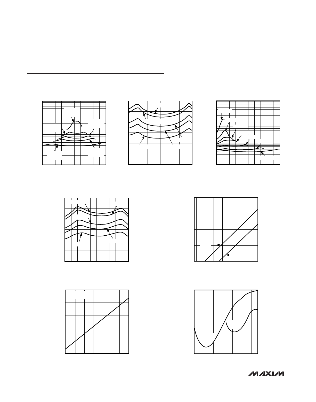
Typical Operating Characteristics
(VCC= 5V, VEE= -5V, V
GND
= 0V, TA= +25°C, unless otherwise noted.)
ON-RESISTANCE vs. VX, VY, V
(DUAL SUPPLIES)
1000
V
CC
V
EE
VCC = 2V,
= -2V
V
(Ω)
100
ON
R
EE
VCC = 5V,
= -5V
V
EE
10
-5 01234-4 -3 -2 -1 5
VX, VY, VZ (V)
130
110
90
(Ω)
70
ON
R
50
30
10
02.01.50.5 1.0 2.5 3.0 3.5 4.0 4.5 5.0
vs. V
65
55
45
(Ω)
35
ON
R
25
TA = -40°C
15
5
-5 -1-2-4-3 012345
= 1.2V,
= -1.2V
Z
VCC = 2.7V,
= -2.7V
V
EE
VCC = 3.3V,
= -3.3V
V
EE
MAX4581/2/3 toc01
ON-RESISTANCE
, VY, VZ AND TEMPERATURE
vs. V
X
(SINGLE SUPPLY)
TA = +85°C
TA = +25°C
TA = -40°C
VX, VY, VZ (V)
TA = +70°C
MAX4581toc04
TA = 0°C
ON-RESISTANCE
, VY, VZ AND TEMPERATURE
X
(DUAL SUPPLIES)
TA = +85°C
TA = +70°C
TA = +25°C
TA = 0°C
VX, VY, VZ (V)
ON-RESISTANCE vs. VX, VY, V
10,000
(Ω)
R
ON
1000
100
10
VCC = 1.2V
010234567891
MAX4581toc02
OFF-LEAKAGE
vs. TEMPERATURE
100
VCC = 5.5V
= -5.5V
V
EE
10
1
OFF LEAKAGE (nA)
IX, IY, I
0.1
0.01
Z
-50 12525-25 0 7550 100
TEMPERATURE (°C)
(SINGLE SUPPLY)
VCC = 2V
VCC = 2.7V
VCC = 3.3V
VX, VY, VZ (V)
IX_, IY_, I
VCC = 5V
Z_
Z
MAX4581 toc03
VCC = 7.5V
VCC = 10V
MAX4581/2/3-05
ON-LEAKAGE
vs. TEMPERATURE
100,000
VCC = 5.5V
= -5.5V
V
10,000
ON LEAKAGE (pA)
EE
1000
100
10
1
-50 12525-25 0 7550 100
TEMPERATURE (°C)
MAX4581/2/3-toc-6
CHARGE INJECTION vs. VX, VY, V
1.5
1.0
0.5
0
-0.5
Q (pC)
-1.0
-1.5
-2.0
-2.5
VCC = 5V
= -5V
V
EE
-5 -3 -2 -1 0-4 12345
VCC = 5V
V
VX, VY, VZ (V)
= 0V
EE
Z
MAX4581-07

MAX4581/MAX4582/MAX4583
Low-Voltage, CMOS Analog
Multiplexers/Switches
_______________________________________________________________________________________
7
Typical Operating Characteristics (continued)
(VCC= 5V, VEE= -5V, V
GND
= 0V, TA= +25°C, unless otherwise noted.)
100
VCC = 5V
V
EE
V
A
10
(nA)
EE
1
, I
CC
I
0.1
0.01
-50 12525-25 0 7550 100
100
600Ω IN AND OUT
10
1
THD (%)
0.1
0.01
10 1k 10k100 100k
SUPPLY CURRENT
vs. TEMPERATURE
= -5V
, VB,VC,V
TOTAL HARMONIC DISTORTION
= 0V, 5V
ENABLE
I
CC
TEMPERATURE (°C)
vs. FREQUENCY
FREQUENCY (Hz)
MAX4581/2/3-08
I
EE
MAX4581-10
0
FREQUENCY RESPONSE
-10
ON-LOSS
-20
-30
-40
-50
-60
LOSS (dB)
-70
-80
-90
-100
-110
-120
0.1 10 1001
V
CC
1
-1
10
-2
10
-3
10
-4
10
-5
10
(A)
CC
-6
I
10
-7
10
-8
10
-9
10
-10
10
-11
10
02314657891110 12
OFF-LOSS
ON-PHASE
FREQUENCY (MHz)
CURRENT vs. LOGIC LEVEL
, VB, VC, V
(V
A
V
V
= 5V
CC
VA, VB, VC, V
ENABLE
ENABLE
= 12V
CC
)
MAX4581-09
120
100
80
60
PHASE (DEGREES)
40
20
0
-20
-40
-60
-80
-110
-120
MAX4581-11
LOGIC-LEVEL THRESHOLD vs. V
3.0
2.5
(V)
2.0
ENABLE
, V
1.5
C
, V
B
, V
A
1.0
V
0.5
0
0 2341576 8 9 101112
VCC (V)
CC
MAX4581toc12

MAX4581/MAX4582/MAX4583
Low-Voltage, CMOS Analog
Multiplexers/Switches
8 _______________________________________________________________________________________
__________Applications Information
Power-Supply Considerations
Overview
The MAX4581/MAX4582/MAX4583 construction is typical of most CMOS analog switches. They have three
supply pins: V
CC
, VEE, and GND. VCCand VEEare used
to drive the internal CMOS switches and set the limits of
the analog voltage on any switch. Reverse ESDprotection diodes are internally connected between
each analog-signal pin and both VCCand VEE. If any
analog signal exceeds VCCor VEE, one of these diodes
Pin Description
Note: Input and output pins are identical and interchangeable. Any may be considered an input or output; signals pass equally well
in both directions.
PIN
MAX4581 MAX4582 MAX4583
PDIP, SO,
TSSOP
13, 14,
15, 12,
1, 5, 2, 4
——
——
— — 3 1 15 13 Y Analog Switch “Y” Output
— — — — 13 11 X1 Analog Switch “X” Normally Open Input
— — — — 12 10 X0 Analog Switch “X” Normally Closed Input
— — — — 1 15 Y1 Analog Switch “Y” Normally Open Input
— — — — 2 16 Y0 Analog Switch “Y” Normally Open Input
— — — — 3 1 Z1 Analog Switch “Z” Normally Open Input
— — — — 5 3 Z0 Analog Switch “Z” Normally Open Input
— — — — 4 2 Z Analog Switch “Z” Output
16 14 16 14 16 14 V
11 9 10 8 11 9 A Digital Address “A” Input
10 8 9 7 10 8 B Digital Address “B” Input
——————EPE xp osed P ad ( TQ FN onl y) . C onnect E P to V
TQFN-EP
11, 12,
13, 10,
15, 3,
16, 2
3 1 13 11 14 12 X Analog Switch “X” Output
9 7 — — 9 7 C Digital Address “C” Input
868686GND
757575V
6 4 6 4 6 4 ENABLE
PDIP, SO,
TSSOP
— — — — X0–X7 Analog Switch Inputs 0–7
12, 14,
15, 11
1, 5, 2,
4
TQFN-EP
10, 12,
13, 9
15, 3,
16, 2
PDIP, SO,
TSSOP
——
——
TQFN-EP
NAME FUNCTION
X0, X1,
X2, X3
Y0, Y1,
Y2, Y3
CC
EE
Analog Switch “X” Inputs 0–3
Analog Switch “Y” Inputs 0–3
Positive Analog and Digital Supply-Voltage
Input
Ground. Connect to digital ground. (Analog
signals have no ground reference; they are
limited to V
Negative Analog Supply-Voltage Input.
Connect to GND for
single-supply operation.
Digital Enable Input. Normally connected to
GND.
and VEE.)
CC
C C
.

MAX4581/MAX4582/MAX4583
Low-Voltage, CMOS Analog
Multiplexers/Switches
_______________________________________________________________________________________ 9
XH
Table 1. Truth Table/Switch Programming
X X All switches open All switches open All switches open
L L X–X0
X–X0,
Y–Y0
X–X0,
Y–Y0,
Z–Z0
LL
L H X–X1
X–X1,
Y–Y1
X–X1,
Y–Y0,
Z–Z0
LL
H H X–X3
X–X3,
Y–Y3
X–X1,
Y–Y1,
Z–Z0
H L X–X2
X–X2,
Y–Y2
X–X0,
Y–Y1,
Z–Z0
LL
LL
L H X–X5
X–X1,
Y–Y1
X–X1,
Y–Y0,
Z–Z1
L L X–X4
X–X0,
Y–Y0
X–X0,
Y–Y0,
Z–Z1
HL
HL
H H X–X7
X–X3,
Y–Y3
X–X1,
Y–Y1,
Z–Z1
H L X–X6
X–X2,
Y–Y2
X–X0,
Y–Y1,
Z–Z1
HL
HL
X = Don’t care
*
C not present on MAX4582.
Note: Input and output pins are identical and interchangeable. Either may be considered an input or output; signals pass equally
well in either direction.
ON SWITCHESSELECT INPUTS
B A MAX4581 MAX4582 MAX4583C*
ENABLE
INPUT
will conduct. During normal operation, these and other
reverse-biased ESD diodes leak, forming the only current drawn from VCCor VEE.
Virtually all the analog leakage current comes from the
ESD diodes. Although the ESD diodes on a given signal pin are identical and therefore fairly well balanced,
they are reverse biased differently. Each is biased by
either VCCor VEEand the analog signal. This means
their leakages will vary as the signal varies. The
differ-
ence
in the two diode leakages to the VCCand V
EE
pins constitutes the analog-signal-path leakage current.
All analog leakage current flows between each pin and
one of the supply terminals, not to the other switch terminal. This is why both sides of a given switch can
show leakage currents of either the same or opposite
polarity.
There is no connection between the analog-signal
paths and GND.
VCCand GND power the internal logic and logic-level
translators, and set the input logic limits. The logic-level
translators convert the logic levels into switched V
CC
and VEEsignals to drive the gates of the analog signals. This drive signal is the only connection between
the logic supplies and signals and the analog supplies.
VCCand VEEhave ESD-protection diodes to GND.
The logic-level thresholds are TTL/CMOS compatible
when VCCis +5V. As VCCrises, the threshold increases

MAX4581/MAX4582/MAX4583
slightly, so when VCCreaches +12V the threshold is
about 3.1V (above the TTL-guaranteed high-level minimum of 2.8V, but still compatible with CMOS outputs).
Bipolar Supplies
These devices operate with bipolar supplies between
±2V and ±5V. The VCCand VEEsupplies need not be
symmetrical, but their sum cannot exceed the +13V
absolute maximum rating
Single Supply
These devices operate from a single supply between
+2V and +12V when V
EE
is connected to GND. All of
the bipolar precautions must be observed. At room
temperature, they actually “work” with a single supply
near or below +1.7V, although as supply voltage
decreases, switch on-resistance and switching times
become very high.
Overvoltage Protection
Proper power-supply sequencing is recommended for
all CMOS devices. Do not exceed the absolute maximum ratings because stresses beyond the listed ratings can cause permanent damage to the devices.
Always sequence VCCon first, then VEE, followed by
the logic inputs and analog signals. If power-supply
sequencing is not possible, add two small signal diodes
(D1, D2) in series with the supply pins for overvoltage
protection (Figure 1).
Adding diodes reduces the analog-signal range to one
diode drop below VCCand one diode drop above VEE,
but does not affect the devices’ low switch resistance
and low leakage characteristics. Device operation is
unchanged, and the difference between V
CC
and V
EE
should not exceed 13V. These protection diodes are
not recommended when using a single supply if signal
levels must extend to ground.
High-Frequency Performance
In 50Ω systems, signal response is reasonably flat up
to 50MHz (see
Typical Operating Characteristics
).
Above 20MHz, the on response has several minor
peaks which are highly layout dependent. The problem
is not turning the switch on, but turning it off. The offstate switch acts like a capacitor and passes higher
frequencies with less attenuation. At 10MHz, off isolation is about -50dB in 50Ω systems, becoming worse
(approximately 20dB per decade) as frequency increases. Higher circuit impedances also degrade off
isolation. Adjacent channel attenuation is about 3dB
above that of a bare IC socket and is entirely due to
capacitive coupling.
Pin Nomenclature
The MAX4581/MAX4582/MAX4583 are pin-compatible
with the industry-standard 74HC4051/74HC4052/
74HC4053 and the MAX4051/MAX4052/MAX4053.
They function identically and have identical logic diagrams, although these parts differ electrically.
The pin designations and logic diagrams in this data
sheet conform to the original 1972 specifications published by RCA for the CD4051/CD4052/CD4053. These
designations differ from the standard Maxim switch and
mux designations as found all other Maxim data sheets
(including the MAX4051/MAX4052/MAX4053) and may
cause confusion. Designers who feel more comfortable
with Maxim’s standard designations are advised that
the pin designations and logic diagrams on the
MAX4051/MAX4052/MAX4053 data sheet may be freely
applied to the MAX4581/MAX4582/MAX4583.
Low-Voltage, CMOS Analog
Multiplexers/Switches
10 ______________________________________________________________________________________
Figure 1. Overvoltage Protection Using External Blocking
Diodes
V
CC
D1
EXTERNAL
BLOCKING DIODE
V
CC
*
X, Y, Z X_, Y_, Z_
*
V
EE
V
EE
*
*
D2
EXTERNAL
BLOCKING DIODE
*INTERNAL PROTECTION DIODES
MAX4581
MAX4582
MAX4583

MAX4581/MAX4582/MAX4583
Low-Voltage, CMOS Analog
Multiplexers/Switches
______________________________________________________________________________________ 11
Figure 2. Address Transition Times
______________________________________________Test Circuits/Timing Diagrams
V
VA, VB, VC
50Ω
V
, V
A
B
50Ω
A
B
C
ENABLE
A
B
ENABLE
CC
V
CC
MAX4581
GND
V
CC
V
CC
X1, X2, Y1, Y2
MAX4582
GND
V
V
V
V
X1–X6
EE
EE
X
X3, Y3
EE
EE
0
X, Y
VA, VB, V
X0
X7
X
V
CC
V
EE
V
OUT
35pF
300Ω
VA, V
, Y
0
300Ω
V
CC
V
EE
V
OUT
35pF
V
CC
C
50%
0V
V
X0
90%
0V
V
OUT
V
X7
t
TRANS
V
CC
B
50%
90%
t
TRANS
0V
V
,
X0
V
Y0
90%
0V
V
OUT
,
V
X3
V
Y3
t
TRANS
90%
t
TRANS
V
CC
V
V
, VB, V
A
C
A, B, C
CC
50Ω
MAX4583
ENABLE
GND
V
= 0V FOR SINGLE-SUPPLY OPERATION.
EE
TEST EACH SECTION INDIVIDUALLY.
X1, Y1, Z1
X2, Y2, Z2
X, Y, Z
V
EE
V
EE
300Ω
V
OUT
CC
C
0V
,
V
X0
,
V
Y0
V
Z0
0V
V
,
X1
,
V
Y1
V
Z1
t
TRANS
VA, VB, V
V
EE
V
CC
V
OUT
35pF
V
50%
90%
90%
t
TRANS

MAX4581/MAX4582/MAX4583
Low-Voltage, CMOS Analog
Multiplexers/Switches
12 ______________________________________________________________________________________
Figure 3. Inhibit Switching Times
_________________________________Test Circuits/Timing Diagrams (continued)
V
CC
V
CC
V
X1–X7
EE
X0
V
CC
V
X
OUT
35pF
V
ENABLE
50Ω
A
B
C
MAX4581
ENABLE
GND
300Ω
V
EE
V
CC
V
CC
A
B
X0, Y0
X1–X3, Y1–Y3
V
CC
MAX4582
V
ENABLE
50Ω
ENABLE
GND
X, Y
V
EE
300Ω
V
EE
35pF
V
OUT
V
V
Enable
V
OUT
Enable
V
OUT
V
CC
50%
0V
V
X0
90%
90%
0V
t
ON
V
CC
50%
t
OFF
0V
V
,
X0
V
Y0
90%
90%
0V
t
ON
t
OFF
V
V
ENABLE
50Ω
A
B
C
ENABLE
CC
V
CC
MAX4583
GND
X1, Y1, Z1
X0, Y0, Z0
X, Y, Z
V
EE
V
EE
300Ω
V
CC
V
EE
V
OUT
35pF
V
Enable
V
OUT
V
VX0,
V
V
VX1,
V
V
CC
50%
0V
,
Y0
Z0
90%
,
Y1
Z1
t
ON
VEE = 0V FOR SINGLE-SUPPLY OPERATION.
TEST EACH SECTION INDIVIDUALLY.
90%
t
OFF

MAX4581/MAX4582/MAX4583
Low-Voltage, CMOS Analog
Multiplexers/Switches
______________________________________________________________________________________ 13
Figure 4. Break-Before-Make Interval
Figure 5. Charge Injection
_________________________________Test Circuits/Timing Diagrams (continued)
V
CC
VA, VB, V
50Ω
C
A
B
C
V
CC
MAX4581
ENABLE
GND
V
V
V
CC
VA, VB, V
50Ω
C
A, B, C
V
CC
X0, X1, Y0,
Y1, Z0, Z1
MAX4583
ENABLE
GND
V
V
VEE = 0V FOR SINGLE-SUPPLY OPERATION.
TEST EACH SECTION INDIVIDUALLY.
X0–X7
EE
EE
X, Y, Z
EE
EE
V
CC
VA, V
V
CC
B
50Ω
A
B
V
CC
X0–X3,
Y0–Y3
V
CC
MAX4582
V
35pF
35pF
OUT
VA, VB, V
V
OUT
V+
C
0V
, VY, V
V
X
Z
V
OUT
0V
X
300Ω
V
CC
300Ω
ENABLE
50%
t
BBM
GND
X, Y
V
EE
300Ω
V
EE
t
< 20ns
R
< 20ns
t
F
80%
35pF
V
OUT
V
CC
V
CC
CHANNEL
SELECT
V
ENABLE
V
= 0V FOR SINGLE-SUPPLY OPERATION.
EE
TEST EACH SECTION INDIVIDUALLY.
A
B
C
ENABLE
50Ω
X_, Y_, Z_
MAX4581
MAX4582
MAX4583
GND
V
V
X, Y, Z
EE
EE
= 1000pF
C
L
V
V
Enable
V
OUT
CC
0V
V
OUT
∆ V
IS THE MEASURED VOLTAGE DUE TO CHARGE
OUT
TRANSFER ERROR Q WHEN THE CHANNEL TURNS OFF.
Q = ∆ V
X C
OUT
L
∆ V
OUT

MAX4581/MAX4582/MAX4583
Low-Voltage, CMOS Analog
Multiplexers/Switches
14 ______________________________________________________________________________________
Figure 6. Off Isolation, On Loss, and Crosstalk
Figure 7. Capacitance
_________________________________Test Circuits/Timing Diagrams (continued)
V
10nF
CC
NETWORK
MEAS.
ANALYZER
50Ω
50Ω 50Ω
50Ω
REF.
OFF-ISOLATION = 20log
ON-LOSS = 20log
CROSSTALK = 20log
V
V
V
OUT
V
OUT
V
OUT
V
IN
IN
IN
V
IN
CHANNEL
SELECT
V
CC
A
B
C
X_, Y_, Z_
MAX4581
MAX4582
V
MAX4583
ENABLE
GND
MEASUREMENTS ARE STANDARDIZED AGAINST SHORT AT SOCKET TERMINALS.
OFF-ISOLATION IS MEASURED BETWEEN COM AND "OFF" NO TERMINAL ON EACH SWITCH.
ON-LOSS IS MEASURED BETWEEN COM AND "ON" NO TERMINAL ON EACH SWITCH.
CROSSTALK (MAX4582/MAX4583) IS MEASURED FROM ONE CHANNEL (A, B, C) TO ALL OTHER CHANNELS.
SIGNAL DIRECTION THROUGH SWITCH IS REVERSED; WORST VALUES ARE RECORDED.
10nF
V
V
X, Y, Z
EE
EE
OUT
V
CC
V
CC
CHANNEL
SELECT
A
B
C
ENABLE
X_, Y_, Z_
MAX4581
MAX4582
MAX4583
GND
V
V
X, Y, Z
EE
EE
1MHz
CAPACITANCE
ANALYZER

MAX4581/MAX4582/MAX4583
Low-Voltage, CMOS Analog
Multiplexers/Switches
______________________________________________________________________________________ 15
Ordering Information (continued)
+
Denotes a lead(Pb)-free/RoHS-compliant package.
/V Denotes an automotive qualified part.
T = Tape and reel.
*
EP = Exposed pad.
Pin Configurations/Functional Diagrams (continued)
BOTTOM VIEW
X1 X0 X3
11 10 9
12
X2
13
V
14
CC
X4
15
X6
16
+
*CONNECT EXPOSED PAD TO V
MAX4581
1234
X7 X5
X
TQFN
CC
PART TEMP RANGE
MAX4581CEE+ 0°C to +70°C 16 QSOP —
MAX4581EPE+ -40°C to +85°C 16 PDIP —
MAX4581ESE+ -40°C to +85°C 16 Narrow SO —
MAX4581EUE+ -40°C to +85°C 16 TSSOP —
MAX4581EEE+ -40°C to +85°C 16 QSOP —
MAX4581ETE+ -40°C to +85°C 16 TQFN-EP* AGH
MAX4581ASE+ -40°C to +125°C 16 Narrow SO —
MAX4581AUE+ -40°C to +125°C 16 TSSOP —
MAX4582CPE+ 0°C to +70°C 16 PDIP —
MAX4582CSE+ 0°C to +70°C 16 Narrow SO —
MAX4582CUE+ 0°C to +70°C 16 TSSOP —
MAX4582CEE+ 0°C to +70°C 16 QSOP —
MAX4582EPE+ -40°C to +85°C 16 PDIP —
MAX4582ESE+ -40°C to +85°C 16 Narrow SO —
MAX4582EUE+ -40°C to +85°C 16 TSSOP —
A
*EP
EN
PINPACKAGE
B
C
GND
V
X2
13
V
14
CC
Y0
15
Y2
EE
16
++
8
7
6
5
TOP
MARK
X1
12
1234
Y
X0 X3
X
11 10 9
A
8
B
7
MAX4582
*EP
Y3 Y1
TQFN TQFN
EN
GND
6
V
5
Y
13
V
14
CC
Y1
15
Y0
EE
16
PART TEMP RANGE
MAX4582EEE+ -40°C to +85°C 16 QSOP —
MAX4582ETE+ -40°C to +85°C 16 TQFN-EP* AGH
MAX4582ASE+ -40°C to +125°C 16 Narrow SO —
MAX4582AUE/V+T -40°C to +125°C 16 TSSOP —
MAX4583CPE+ 0°C to +70°C 16 PDIP —
MAX4583CSE+ 0°C to +70°C 16 Narrow SO —
MAX4583CUE+ 0°C to +70°C 16 TSSOP —
MAX4583CEE+ 0°C to +70°C 16 QSOP —
MAX4583EPE+ -40°C to +85°C 16 PDIP —
MAX4583ESE+ -40°C to +85°C 16 Narrow SO —
MAX4583EUE+ -40°C to +85°C 16 TSSOP —
MAX4583EEE+ -40°C to +85°C 16 QSOP —
MAX4583ETE+ -40°C to +85°C 16 TQFN–EP* AGH
MAX4583ASE+ -40°C to +125°C 16 Narrow SO —
MAX4583AUE+ -40°C to +125°C 16 TSSOP —
X1 X0
X
12
11 10 9
A
MAX4583
*EP
1234
Z1
Z0
Z
EN
PINPACKAGE
B
8
C
7
GND
6
V
5
EE
TOP
MARK

MAX4581/MAX4582/MAX4583
Low-Voltage, CMOS Analog
Multiplexers/Switches
16 ______________________________________________________________________________________
Package Information
For the latest package outline information and land patterns
(footprints), go to www.maxim-ic.com/packages
. Note that a
“+”, “#”, or “-” in the package code indicates RoHS status only.
Package drawings may show a different suffix character, but
the drawing pertains to the package regardless of RoHS status.
PACKAGE
TYPE
PACKAGE
CODE
OUTLINE NO.
LAND
PATTERN NO.
16 PDIP P16+1
21-0043
—
16 Narrow SO S16+1
21-0041 90-0097
16 TSSOP U16+2
21-0066 90-0117
16 QSOP E16+4
21-0055 90-0167
16 TQFN T1633+5
21-0136
90-0032
Chip Information
PROCESS: BICMOS
TRANSISTOR COUNT: 219

Maxim cannot assume responsibility for use of any circuitry other than circuitry entirely embodied in a Maxim product. No circuit patent licenses are
implied. Maxim reserves the right to change the circuitry and specifications without notice at any time. The parametric values (min and max limits) shown in
the Electrical Characteristics table are guaranteed. Other parametric values quoted in this data sheet are provided for guidance.
17
____________________Maxim Integrated Products, 120 San Gabriel Drive, Sunnyvale, CA 94086 408-737-7600
© 2012 Maxim Integrated Products Maxim is a registered trademark of Maxim Integrated Products, Inc.
MAX4581/MAX4582/MAX4583
Low-Voltage, CMOS Analog
Multiplexers/Switches
Revision History
REVISION
NUMBER
5 6/07 Various changes —
6 3/12
REVISION
DATE
DESCRIPTION
Updated TQFN, PDIP, and lead-free packaging options; updated temperature
ranges
PAGES
CHANGED
1–7, 15, 16
 Loading...