

For free samples & the latest literature: http://www.maxim-ic.com, or phone 1-800-998-8800.
For small orders, phone 1-800-835-8769.
General Description
The MAX4550/MAX4570 serial-interface, programmable, dual 4x2 audio/video crosspoint switches are ideal
for multimedia applications. Each device contains two
identical crosspoint switch arrays, each with four inputs
and two outputs. To improve off-isolation, use the additional crosspoint inputs SA and SB as shunts. Each output is selectively programmable for clickless or regular
mode operation. A set of internal resistive voltagedividers supplies DC bias for each output when using
AC-coupled inputs. Additionally, four auxiliary outputs
control additional circuitry via the MAX4550/MAX4570’s
2-wire or 3-wire interface.
The MAX4550/MAX4570 feature 80Ω on-resistance, 10Ω
on-resistance matching between channels, 5Ω onresistance flatness, and 0.014% total harmonic distortion. Additionally, they feature off-isolation of at least
-110dB in the audio frequency range and -78dB at
4MHz, with -95dB crosstalk in the audio frequency
range and -54dB at 4MHz. The MAX4550 uses a 2-wire
I2C-compatible serial interface, while the MAX4570
uses a 3-wire SPI™/QSPI™ or MICROWIRE™-compatible serial interface. These parts are available in 28-pin
SSOP and wide SO packages and are tested over
either the commercial (0°C to +70°C) or extended
(-40°C to +85°C) operating temperature range.
Applications
Set-Top Boxes
PC Multimedia Boards
High-End Audio Systems
Video Conferencing Systems
Features
♦ Selectable Soft Switching Mode for Clickless
Audio Operation
♦ 43Ω Typical On-Resistance (±5V Supplies)
♦ 5Ω Typical On-Resistance Matching Between
Channels
♦ 4Ω Typical On-Resistance Flatness
♦ 0.014% Total Harmonic Distortion with 1kΩ Load
♦ -110dB Off-Isolation at 20kHz
-78dB Off-Isolation at 4MHz
♦ -95dB Crosstalk at 20kHz
-54dB Crosstalk at 4MHz
♦ Serial Interface
2-Wire, Fast-Mode, I
2
C-Compatible (MAX4550)
3-Wire, SPI/QSPI/MICROWIRE-Compatible
(MAX4570)
♦ Four Auxiliary Outputs that Extend µP Ports
♦ Single-Supply Operation: +2.7V to +5.5V
Dual-Supply Operation: ±2.7V to ±5.5V
MAX4550/MAX4570
Serially Controlled, Dual 4x2, Clickless
Audio/Video Analog Crosspoint Switches
________________________________________________________________
Maxim Integrated Products
1
28
27
26
25
24
23
22
21
20
19
18
17
16
15
1
2
3
4
5
6
7
8
9
10
11
12
13
14
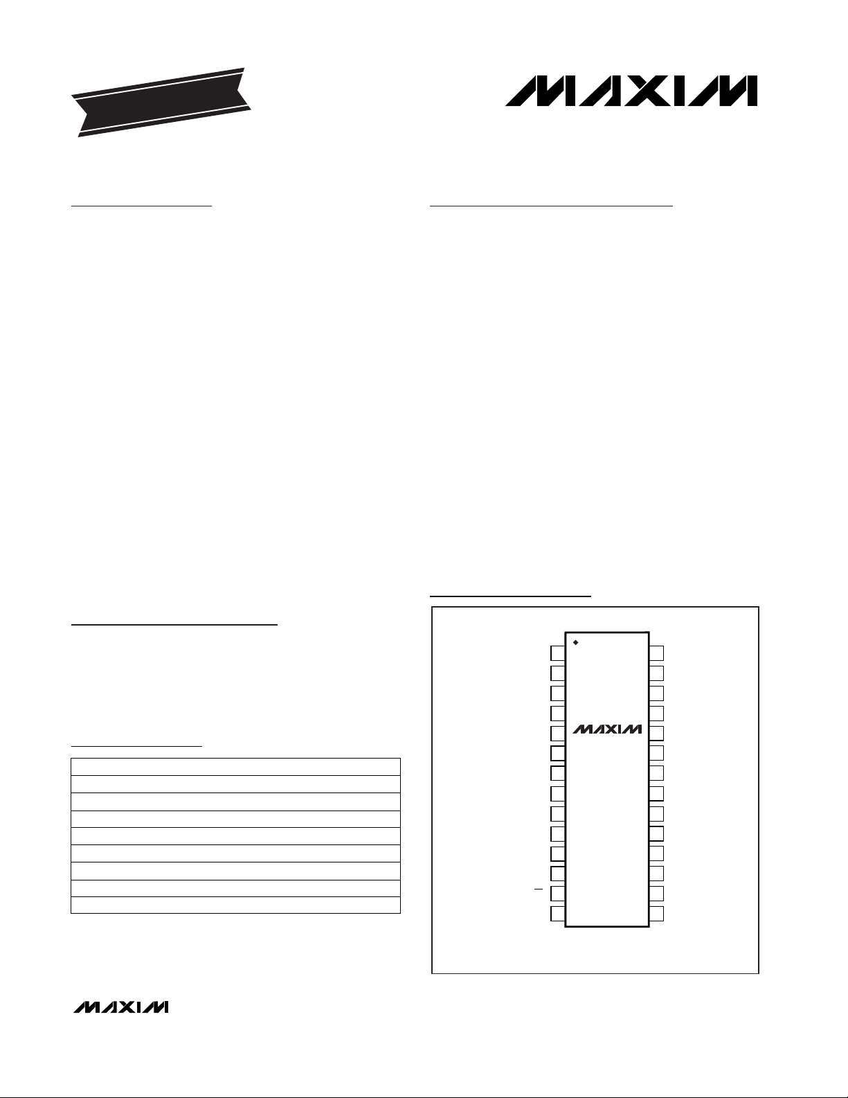
SA
NO2B
NO2A
VV+
NO1B
SDA (DIN)
NO1A
GND
COM1A
Q3
COM1B
Q2
A1 (DOUT)
SCL (SCLK)
A0 (CS)
Q1
COM2B
( ) ARE FOR MAX4570.
Q0
COM2A
V+
NO4B
NO4A
BIASL
BIASH
NO3B
NO3A
SB
SO/SSOP
TOP VIEW
MAX4550
MAX4570
19-1397; Rev 0; 10/98
PART
MAX4550CAI
MAX4550CWI
MAX4550EAI -40°C to +85°C
0°C to +70°C
0°C to +70°C
TEMP. RANGE PIN-PACKAGE
28 SSOP
28 Wide SO
28 SSOP
EVALUATION KIT
AVAILABLE
Functional Diagram appears at end of data sheet.
Pin Configuration
Ordering Information
MAX4550EWI -40°C to +85°C 28 Wide SO
MAX4570CAI
MAX4570CWI
MAX4570EAI -40°C to +85°C
0°C to +70°C
0°C to +70°C 28 SSOP
28 Wide SO
28 SSOP
MAX4570EWI -40°C to +85°C 28 Wide SO
I2C is a trademark of Philips Corp.
SPI/QSPI are trademarks of Motorola, Inc.
MICROWIRE is a trademark of National Semiconductor Corp.
Channel-to-Channel Crosstalk V
CTA(A)
ICOM_ _ = 1mA
MAX4550/MAX4570
Serially Controlled, Dual 4x2, Clickless
Audio/Video Analog Crosspoint Switches
2 _______________________________________________________________________________________
ABSOLUTE MAXIMUM RATINGS
ANALOG ELECTRICAL CHARACTERISTICS—Dual Supplies
(V+ = +5V ±5%, V- = -5V ±5%, TA= T
MIN
to T
MAX
, unless otherwise noted. Typical values are at TA= +25°C.) (Note 2)
Stresses beyond those listed under “Absolute Maximum Ratings” may cause permanent damage to the device. These are stress ratings only, and functional
operation of the device at these or any other conditions beyond those indicated in the operational sections of the specifications is not implied. Exposure to
absolute maximum rating conditions for extended periods may affect device reliability.
Note 1: Signals on NO_ _, S_, or COM_ _ exceeding V+ or V- are clamped by internal diodes. Limit forward-diode current to maxi-
mum current rating.
V+ to GND............................................................... -0.3V to +6V
V+ to V-................................................................-0.3V to +13.2V
V- to GND.................................................................+0.3V to -6V
NO_ _ , S_, BIAS_, COM_ _, Q_, A1, DOUT to GND
(Note 1)...............................................(V- - 0.3V) to (V+ + 0.3V)
CS, SCLK, DIN, SCL, SDA, A0 to GND....................-0.3V to +6V
Continuous Current into Any Terminal..............................±10mA
Peak Current, NO_ _ , S_ , COM_ _
(pulsed at 1ms, 10% duty cycle max) ..........................±40mA
Continuous Power Dissipation (T
A
= +70°C)
28-Pin SSOP (derate 9.52mW/°C above +70°C) .........762mW
28-Pin Wide SO (derate 12.5mW/°C above +70°C) ...1000mW
Operating Temperature Ranges
MAX4550C_I/MAX4570C_I ...............................-0°C to +70°C
MAX4550E_I/MAX4570E_I ..............................-40°C to +85°C
Storage Temperature Range.............................-65°C to +160°C
Lead Temperature (soldering, 10sec).............................+300°C
I
COM_ _
= 4mA,
V
NO_ _
or VS_= ±3.0V,
V+ = 4.75V, V- = -4.75V
CONDITIONS
Ω
43 80
R
ON
On-Resistance
VV- V+
V
NO_ _
,
V
COM_ _
,
V
S_
Analog Signal Range (Note 3)
UNITSMIN TYP MAXSYMBOLPARAMETER
-110
TA= +25°C
TA= T
MIN
to T
MAX
100
I
COM_ _
= 4mA,
V
NO_ _
or VS_= ±3.0V,
V+ = 4.75V, V- = -4.75V
Ω
5 10
∆R
ON
COM_ _ to NO_ _ or S_
On-Resistance Match Between
Channels (Note 4)
TA= +25°C
TA= T
MIN
to T
MAX
10
I
COM_ _
= 4mA;
V
NO_ _
or VS_= ±3.0V, 0;
V+ = 4.75V; V- = -4.75V
Ω
4 5
∆R
FLAT(ON)
COM_ _ to NO_ _ or S_
On-Resistance Flatness
(Note 5)
TA= +25°C
TA= T
MIN
to T
MAX
8
V
NO_ _
or VS_= ±4.5V,
V
COM_
=
–
+
4.5V,
V+ = 5.25V, V- = -5.25V
nA
-1 0.01 1
NO
_(OFF)
NO_ _ or S_ Off-Leakage
Current (Note 6)
TA= +25°C
TA= T
MIN
to T
MAX
-10 10
V
NO_ _
or VS_= ±4.5V,
V
COM_
=
–
+
4.5V,
V+ = 5.25V, V- = -5.25V
nA
-5 0.01 5
I
COM
_(OFF)
COM_ _ Off-Leakage Current
(Note 6)
TA= +25°C
TA= T
MIN
to T
MAX
-10 10
V
NO_ _
or VS_= floating,
V
COM_
= ±4.5V,
V+ = 5.25V, V- = -5.25V
nA
-5 0.01 5
I
COM
_(ON)
COM_ _ On-Leakage Current
(Note 6)
TA= +25°C
TA= T
MIN
to T
MAX
-20 20
V
NO_ _
or VS_= 1V
RMS
, fIN= 20kHz,
RL= 10kΩ, three channels driven at 20kHz
dB-95V
CTA(A)
Channel-to-Channel Crosstalk
VNO= 1V
RMS
, fIN= 20kHz,
RL= 10kΩ, S = GND
dB
-80
V
ISO(A)
Off-Isolation (Note 7)
fIN= 1kHz, RL= 1kΩ, V
NO_
or VS_= 1V
RMS
,
V
NO_
or VS_= 0
%0.014THD+N
Total Harmonic Distortion plus
Noise
Shunt switch on
Shunt switch off
ANALOG SWITCHES
AUDIO PERFORMANCE
MAX4550/MAX4570
Serially Controlled, Dual 4x2, Clickless
Audio/Video Analog Crosspoint Switches
_______________________________________________________________________________________ 3
ANALOG ELECTRICAL CHARACTERISTICS—Dual Supplies (continued)
(V+ = +5V ±5%, V- = -5V ±5%, TA= T
MIN
to T
MAX
, unless otherwise noted. Typical values are at TA= +25°C.) (Note 2)
fIN= 1MHz,
CONDITIONS
pF11C
OFF(NO)
Off-Capacitance
-78
UNITSMIN TYP MAXSYMBOLPARAMETER
Shunt switch on
Shunt switch off
V
NO_ _
or VS_= 1
VRMS
,
fIN= 4MHz, RL= 1kΩ,
S_ = GND
dB
-63
V
ISO(V)
Off-Isolation
RS= 75Ω, RL= 1kΩ MHz14BW0.1dB Bandwidth
V
NO_ _
or V
S_
= 1.5V, RL= 300Ω
V
NO_ _
or V
S_
= 1.5V, RL= 5kΩ
ns200 500t
OFFSD
Turn-Off Time (Note 9)
ns400 900t
ONSD
Turn-On Time (Note 9)
V
NO_ _
or V
S_
= 1.5V ns10 100t
BBM
Break-Before-Make Time
V
NO_ _
or V
S_
= 1.5V, RL= 300Ω
V
NO_ _
or V
S_
= 1.5V, RL= 5kΩ
ms11t
OFFSE
Turn-Off Time
ms36t
ONSE
Turn-On Time
BIASH to BIASL kΩ13 20 27R
BIAS
Bias Network Resistance
Reset condition, V+ = 2.7V to 5.25V µA7 20I+V+ Supply Current (Note 10)
V+
Reset condition, V- = -5.25V to 0 µA-20I-V- Supply Current
V
NO_ _
or VS_= 1
VRMS
, fIN= 4MHz,
R
L
= 10Ω, three channels driven at 4MHz
dB-54V
CT(V)
Channel-to-Channel Crosstalk
V
2.7 5.25
V-
Supply Voltage Range
-5.25 0
ANALOG ELECTRICAL CHARACTERISTICS—Single +5V Supply
(V+ = +5V ±5%, V- = 0, TA= T
MIN
to T
MAX
, unless otherwise noted. Typical values are at TA= +25°C.) (Note 2)
I
COM_ _
= 4mA,
V
NO_ _
or VS_= 3.0V,
V+ = 4.75V
I
COM_ _
= 4mA,
V
NO_ _
or VS_= 3.0V,
V+ = 4.75V
Ω
5 10
∆R
ON
On-Resistance Match Between
Channels (Note 4)
CONDITIONS
V
NO
or VS_= 4.5V, 1V;
V
COM_ _
= 1V, 4.5V;
V+ = 5.25V
nA
-1 0.01 1
I
NO_ _(OFF)
NO_ _ or S_ Off-Leakage
Current (Notes 6, 11)
TA= +25°C
TA= T
MIN
to T
MAX
-10 10
I
COM_ _
= 4mA;
V
NO_ _
or VS_= 1V, 2V,
3V; V+ = 4.75V
Ω
4 10
Ω
60 100
R
ON
On-Resistance
V0 V+
V
NO_ _
,
V
COM_ _
,
V
S_
Analog Signal Range (Note 3)
R
FLAT
On-Resistance Flatness
(Note 5)
TA= +25°C
TA= T
MIN
to T
MAX
15
UNITSMIN TYP MAXSYMBOLPARAMETER
TA= +25°C
TA= +25°C
TA= T
MIN
to T
MAX
130
TA= T
MIN
to T
MAX
10
VIDEO PERFORMANCE
DYNAMIC TIMING WITH CLICKLESS MODE DISABLED (Note 8)
DYNAMIC TIMING WITH CLICKLESS MODE ENABLED (Note 8, Figure 5)
BIAS NETWORKS
POWER SUPPLIES
ANALOG SWITCHES
MAX4550/MAX4570
Serially Controlled, Dual 4x2, Clickless
Audio/Video Analog Crosspoint Switches
4 _______________________________________________________________________________________
ANALOG ELECTRICAL CHARACTERISTICS—Single +5V Supply (continued)
(V+ = +5V ±5%, V- = 0, TA= T
MIN
to T
MAX
, unless otherwise noted. Typical values are at TA= +25°C.) (Note 2)
V
NO_ _
or VS_= floating;
V
COM_ _
= 1V, 4.5V;
V+ = 5.25V
nA
Shunt switch on
-5 0.01 5
I
COM_ _(ON)
COM_ _ On-Leakage Current
(Notes 6, 11)
CONDITIONS
Shunt switch off
-105
TA= +25°C
TA= T
MIN
to T
MAX
-20 20
V
NO_ _
or VS_= 1V
RMS
, fIN=
20kHz, RL= 10kΩ, S = GND
V
NO_ _
or VS_= 1V
RMS
, fIN= 20kHz,
RL= 10kΩ, three channels driven at 20kHz
dB
-80
V
ISO(A)
Off-Isolation (Note 7)
dB-97V
TC(A)
V
NO_ _
or VS_= 4.5V, 1V;
V
COM_ _
= 1V, 4.5V;
V+ = 5.25V
nA
-5 0.01 5
I
COM_ _(OFF)
COM_ _ Off-Leakage Current
(Notes 6, 11)
TA= +25°C
TA= T
MIN
to T
MAX
-10 10
Channel-to-Channel Crosstalk
fIN= 1kHz, RL= 10kΩ, V
NO_ _
or VS_= 1V
RMS
,
V
NO_ _
or VS_= 2.5V
%0.014THD+N
Total Harmonic Distortion plus
Noise
UNITSMIN TYP MAXSYMBOLPARAMETER
-74
V
NO_ _
or VS_= 1V
RMS
, fIN=
4MHz, RL= 1kΩ, S = GND
dB
-61
V
ISO(V)
Off-Isolation (Note 7)
R
SOURCE
= 75Ω, RL= 1kΩ MHz13BW0.1dB Bandwidth
fIN= 1MHz pF11C
OFF(NO)
Off-Capacitance
V
NO_ _
or V
S_
= 1.5V, RL= 5kΩ ns400 900t
ONSD
Turn-On Time (Note 9)
V
NO_ _
or V
S_
= 1.5V, RL= 300Ω ns160 500t
OFFSD
Turn-Off Time (Note 9)
V
NO_ _
or V
S_
= 1.5V ns10 100t
BBM
Break-Before-Make Time
V
NO_ _
or V
S_
= 1.5V, RL= 5kΩ ms43t
ONSE
Turn-On Time
V
NO_ _
or V
S_
= 1.5V, RL= 300Ω ms14t
OFFSE
Turn-Off Time
BIASH to BIASL kΩ13 20 27R
BIAS
Bias Network Resistance
V
NO_ _
or VS_= 1V
RMS
, fIN= 4MHz,
RL= 10kΩ, three channels driven at 4MHz
dB-52V
TC(V)
Channel-to-Channel Crosstalk
ANALOG ELECTRICAL CHARACTERISTICS—Single +3V Supply
(V+ = +3V ±10%, V- = 0, TA= T
MIN
to T
MAX
, unless otherwise noted. Typical values are at TA= +25°C.) (Note 2)
I
COM_ _
= 4mA,
V
NO_ _
or VS_= 1V,
V+ = 2.7V
CONDITIONS
Ω
106 180
R
ON
On-Resistance
V0 V+
V
NO_ _
,
V
COM_ _
,
V
S_
Analog Signal Range (Note 3)
UNITSMIN TYP MAXSYMBOLPARAMETER
TA= +25°C
TA= T
MIN
to T
MAX
220
ANALOG SWITCHES
Shunt switch on
Shunt switch off
AUDIO PERFORMANCE
VIDEO PERFORMANCE
DYNAMIC TIMING WITH CLICKLESS MODE DISABLED (Note 8)
DYNAMIC TIMING WITH CLICKLESS MODE ENABLED (Note 8, Figure 5)
BIAS NETWORKS
I
SINK
= 6mA
MAX4550/MAX4570
Serially Controlled, Dual 4x2, Clickless
Audio/Video Analog Crosspoint Switches
_______________________________________________________________________________________ 5
INTERFACE I/O CHARACTERISTICS
(V+ = +2.7V to +5.5V, V- = 0 to -5.5V, TA= T
MIN
to T
MAX
, unless otherwise noted. Typical values are at TA= +25°C.) (Note 2)
I
SOURCE
= 1mA to GND, V+ = 4.75V
CONDITIONS
4.45 4.65
UNITSMIN TYP MAXSYMBOLPARAMETER
V
2.3 2.5
V
OH
Output High Voltage
I
SOURCE
= 0.5mA to GND, V+ = 2.7V
V
0.5 1.0
V
OL
Output Low Voltage
I
SINK
= 12mA, V+ = 4.75V
0.5 1.0I
SINK
= 6mA, V+ = 2.7V
V+ > 3.6V 3.0
V+ > 3.6V 0.8
V+ < 3.6V
V
2.0
V
IH
Input High Voltage
V0.2
V+ < 3.6V
V
HYST
Input Hysteresis
V
NO_ _
= 0 or 5V µA-1 0.01 1I
LEAK
Input Leakage Current (Note 7)
0.4
I
SOURCE
= 0.5mA VV+ - 0.5 V+ - 0.1
I
SINK
= 6mA
V
OH
DOUT Output High Voltage
V
0.8
V
OL
Output Low Voltage
V
0.6
V
IL
Input Low Voltage
kHzDC 400f
SCL
SCL Clock Frequency
µs0.6t
SU:STO
STOP Condition Setup Time
ns100t
SU:DAT
Data Setup Time
µs0 0.9t
HD:DAT
Data Hold Time
µs1.3t
BUF
Bus Free Time between Stop
and Start Condition
µs1.3t
LOW
Clock Low Period
µs0.6t
HIGH
Clock High Period
MHzDC 2.1f
OP
Operating Frequency
ns0f
DH
DIN to SCLK Hold
ns100f
DS
DIN to SCLK Setup
ns20 200f
DO
SCLK Fall to Output Data Valid C
LOAD
= 50pF
ns0f
CSH
CS to SCLK Rise Hold
ns100f
CSS
CS to SCLK Rise Setup
ns
20 + 300
0.1Cb
t
R
SCL/SDA Rise Time
(Note 12)
ns
20 + 300
0.1Cb
t
F
SCL/SDA Fall Time
(Note 12)
pF5C
NO
Input Capacitance
V+ = 4.75V
V+ = 2.7V
SPI TIMING (V+ = +4.75V to +5.25V, Figures 3, 4)
I2C TIMING (V+ = +4.75V to +5.25V, Figures 1, 2)
DIGITAL OUTPUTS (DOUT, SDA)
DIGITAL INPUTS (SCK, DIN, CS, SCL, SDA)
AUXILIARY OUTPUTS

MAX4550/MAX4570
Serially Controlled, Dual 4x2, Clickless
Audio/Video Analog Crosspoint Switches
6 _______________________________________________________________________________________
INTERFACE I/O CHARACTERISTICS (continued)
(V+ = +2.7V to +5.5V, V- = 0 to -5.5V, TA= T
MIN
to T
MAX
, unless otherwise noted. Typical values are at TA= +25°C.) (Note 2)
CONDITIONS UNITSMIN TYP MAXSYMBOLPARAMETER
ns200t
CL
SCLK Pulse Width High
ns200t
CH
SCLK Pulse Width Low
µs2.0t
R
Rise Time (SCLK, DIN, CS)
µs2.0t
F
Fall Time (SCLK, DIN, CS)
Note 2: The algebraic convention is used in this data sheet; the most negative value is shown in the minimum column.
Note 3: Guaranteed by design. Not subject to production testing.
Note 4: ∆R
ON
= R
ON(MAX)
- R
ON(MIN)
.
Note 5: On-resistance flatness is defined as the difference between the maximum and minimum on-resistance values, as measured
over the specified analog signal range.
Note 6: Leakage parameters are 100% tested at maximum rated temperature, and guaranteed by correlation at T
A
= +25°C.
Note 7: Off-isolation = 20
· log (V
COM_ __
/ V
NO_ _
), V
COM_ _
= output, V
NO_ _
= input to off switch.
Note 8: All timing is measured from the clock’s falling edge preceding the ACK signal for 2-wire, and from CS’s rising edge for
3-wire. Turn-Off Time is defined as the output of the switch for 0.5V change, tested with a 300Ω load to ground. Turn-On
Time is measured with a 5kΩ load resistor to GND. All timing is shown with respect to 20% of V+ and 70% of V+, unless
otherwise noted.
Note 9: Typical values are for MAX4570 only.
Note 10: Supply current can be as high as 2mA per switch during switch transitions in the clickless mode, corresponding to 40mA
total supply transient current requirement.
Note 11: Leakage testing for single-supply operation is guaranteed by testing with dual supplies.
Note 12: Cb = capacitance of one bus line in pF. Tested with Cb = 400pF.
40
44
42
48
46
52
50
54
58
56
60
-5 -3 -2 -1-4 0 1 2 43 5
ON-RESISTANCE vs. V
COM
(DUAL SUPPLIES)
AMX4550/4570-01
V
COM
(V)
R
ON
(Ω)
V± = ±2.7V
V± = ±3.3V
V± = ±4.75V
30
35
40
45
50
55
60
-5 -3 -2 -1-4 0 1 2 43 5
ON-RESISTANCE vs. V
COM
AND TEMPERATURE (DUAL SUPPLIES)
AMX4550/4570-02
V
COM
(V)
R
ON
(Ω)
V± = ±5V
TA = +85°C
TA = +70°C
TA = +25°C
TA = -40°C
50
60
70
80
90
100
110
120
130
0 1 2 3 4 5
ON-RESISTANCE vs. V
COM
(SINGLE SUPPLY)
AMX4550/4570-03
V
COM
(V)
R
ON
(Ω)
V+ = +2.7V
V+ = +3.3V
V+ = +5V
Typical Operating Characteristics
(TA = +25°C, unless otherwise noted.)

MAX4550/MAX4570
Serially Controlled, Dual 4x2, Clickless
Audio/Video Analog Crosspoint Switches
_______________________________________________________________________________________
7
40
45
50
55
60
65
70
75
0 1 2 3 4 5
ON-RESISTANCE vs. V
COM
AND
TEMPERATURE (SINGLE SUPPLY)
AMX4550/4570-04
V
COM
(V)
R
ON
(Ω)
TA = +70°C
TA = +85°C
TA = +25°C
TA = -40°C
V+ = +5V
V- = 0
30
40
35
50
45
65
60
55
70
-40 0-20 20 40 60 80
ON-RESISTANCE vs. TEMPERATURE
AMX4550/4570-05
TEMPERATURE (°C)
R
ON
(Ω)
V+ = +5V
V- = 0
V± = ±5V
0.1
1
10
1000
100
10,000
-40 0-20 20 40 60 80
LEAKAGE CURRENT vs. TEMPERATURE
AMX4550/4570-06
TEMPERATURE (°C)
LEAKAGE CURRENT (pA)
V± = ±5V
COM_ON
NO_OFF
COM_OFF
1
2
5
4
3
9
8
7
6
10
-40 -20 200 40 60 80
SUPPLY CURRENT vs. TEMPERATURE
(DUAL SUPPLIES)
AMX4550/4570-07
TEMPERATURE (°C)
SUPPLY CURRENT (µA)
I+
I-
V+ = ±5V
200
400
300
600
500
800
700
900
1100
1000
1200
2.7 3.5 3.93.1 4.3 4.7 5.1 5.5
TURN-ON/TURN-OFF TIMES vs.
SUPPLY VOLTAGE (SINGLE SUPPLY)
AMX4550/4570-10
V
SUPPLY
(V)
TIME (ns)
t
ON
t
OFF
1
2
5
4
3
9
8
7
6
10
SUPPLY CURRENT vs. TEMPERATURE
(SINGLE SUPPLY)
AMX4550/4570-08
TEMPERATURE (°C)
SUPPLY CURRENT (µA)
-40 -20 200 40 60 80
V+ = +5V
V+ = +2.7V
V- = 0
0
2
8
6
4
16
14
12
10
18
-4 -1-2-3 0 1 2 3 4-5 5
CHARGE INJECTION vs. V
COM
AMX4550/4570-09
V
COM
(V)
Q (pC)
V± = ±5V
V+ = +5V
V- = 0
200
400
300
500
700
600
800
900
1000
2.7 3.5 3.93.1 4.3 4.7 5.1 5.5
TURN-ON/TURN-OFF TIMES vs.
SUPPLY VOLTAGE (DUAL SUPPLIES)
AMX4550/4570-11
V
SUPPLY
(V)
TIME (ns)
t
ON
t
OFF
10
-90
0.5 1 10 100
OFF-ISOLATION AND CROSSTALK
vs. FREQUENCY
-60
-70
-80
0
-10
-20
-30
-40
-50
AMX4550/4570-12
FREQUENCY (MHz)
CROSSTALK (dB)
V± = ±5V
OFF-ISOLATION
CROSSTALK
-30
-130
-100
-110
-120
-40
-50
-60
-70
-80
-90
ISOLATION (dB)
Typical Operating Characteristics (continued)
(TA = +25°C, unless otherwise noted.)

MAX4550/MAX4570
Serially Controlled, Dual 4x2, Clickless
Audio/Video Analog Crosspoint Switches
8 _______________________________________________________________________________________
Typical Operating Characteristics (continued)
(TA = +25°C, unless otherwise noted.)
2
-8
0.5 1 10 100 500
FREQUENCY RESPONSE
-5
-6
-7
1
0
-1
-2
-3
-4
AMX4550/4570-13
FREQUENCY (MHz)
LOSS (1dB/div)
V± = ±5V
0.20
-0.30
0.5 1 2 5 10 20
FREQUENCY RESPONSE
-0.15
-0.20
-0.25
0.15
0.10
0.05
0
-0.05
-0.10
AMX4550/4570-14
FREQUENCY (MHz)
LOSS (dB)
V± = ±5V
0.1
0.001
1 10 100 1000 10,000 100,000
TOTAL HARMONIC DISTORTION
PLUS NOISE vs. FREQUENCY
0.01
AMX4550/4570-15
FREQUENCY (Hz)
THD+NOISE (%)
R
LOAD
= 10kΩ
V± = ±5V
0
500µs/div
COM RISE TIME (SOFT MODE)
200mV/
div
AMX4550/4570-16
V± = ±5V
0
25ns/div
COM TURN-OFF TIME (HARD MODE)
0
COM
0.5V/div
CS
1V/div
AMX4550/4570-19
V± = ±5V
0
500µs/div
COM FALL TIME (SOFT MODE)
200mV/
div
AMX4550/4570-17
V± = ±5V
0
50ns/div
COM TURN-ON TIME (HARD MODE)
0
COM
0.5V/div
CS
1V/div
AMX4550/4570-18
V± = ±5V
0
5ms/div
COM TURN-ON TIME (SOFT MODE)
0
COM
0.5V/div
CS
1V/div
AMX4550/4570-20
V± = ±5V
0
5ms/div
COM TURN-OFF TIME (SOFT MODE)
0
COM
0.5V/div
CS
1V/div
AMX4550/4570-21
V± = ±5V

MAX4550/MAX4570
Serially Controlled, Dual 4x2, Clickless
Audio/Video Analog Crosspoint Switches
_______________________________________________________________________________________ 9
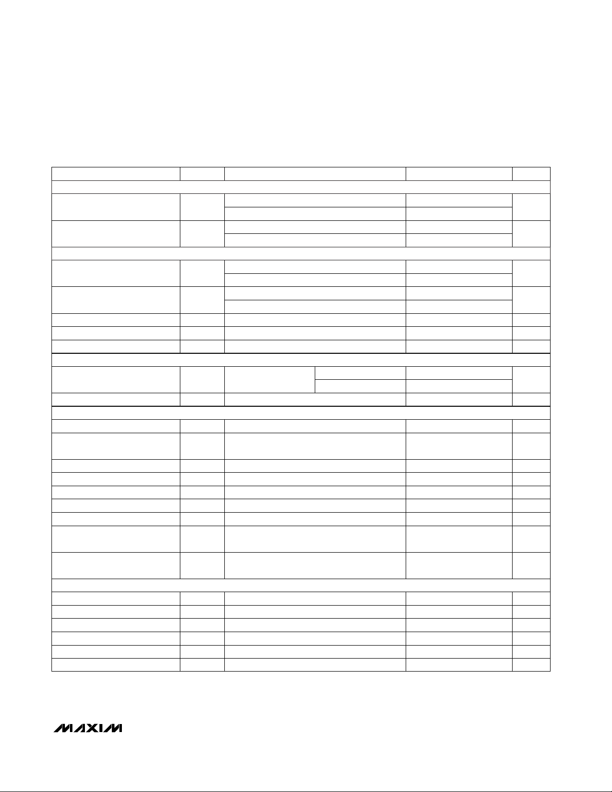
Pin Description
Shunt Input to Crosspoint B. Use for shunt capacitor or AC ground connection to
improve off-isolation, or as an additional input to switch matrix B.
11
Input 3 to Crosspoint A22
Input 3 to Crosspoint B33
NO3A
NO3B
SB
Low Side of Bias Network. Use to give the outputs a DC bias when inputs are
AC-coupled (refer to the
Using the Internal Bias Resistors
section).
55
Input 4 to Crosspoint A66
BIASL
NO4A
BIASH
High Side of Bias Network. Use to give the outputs a DC bias when inputs are
AC-coupled (refer to the
Using the Internal Bias Resistors
section).
44
Positive Supply Voltage. Supply range is +2.7V to +5.25V. Connect pin 8 to pin 24 externally.
8, 248, 24
Output 2 of Crosspoint A99
V+
COM2A
NO4B
Output 2 of Crosspoint B1111
Auxiliary Output 11212
COM2B
Q1
Q0 Auxiliary Output 01010
Input 4 to Crosspoint B77
Chip Select of 3-Wire Interface. Logic low on CS enables serial data to be clocked in to
device. Programming commands are executed on CS’s rising edge.
13—
2-Wire Serial-Interface Clock Input —14
CS
SCL
A0
2-Wire Serial-Interface Data Input. Data is clocked in on SCL’s rising edge.—15
3-Wire Serial-Interface Data Input. Data is clocked in on SCLK’s rising edge.15—
SDA
DIN
SCLK 3-Wire Serial-Interface Clock Input14—
Data Output of 3-Wire Interface. Input data is clocked out and SCLK’s falling edge
delayed by 16 clock cycles. DOUT remains active when CS is high.
16—
Auxiliary Output 21717
DOUT
Q2
A1
Auxiliary Output 3
LSB+1 of 2-Wire Serial-Interface Address Field—13
1919
Output 1 of Crosspoint A2020
Q3
COM1A
COM1B Output 1 of Crosspoint A1818
LSB+2 of 2-Wire Serial-Interface Address Field—16
Ground2121 GND
Input 1 to Crosspoint A2222 NO1A
Input 1 to Crosspoint B2323 NO1B
Negative Supply Voltage. Supply range is from -5.25V to 0.2525 VInput 2 to Crosspoint A2626 NO2A
Input 2 to Crosspoint B2727 NO2B
Shunt Input to Crosspoint A. Use for shunt capacitor or AC ground connection to
improve off-isolation, or as an additional input to switch matrix A.
2828 SA
MAX4550
FUNCTION
MAX4570
NAME
PIN

MAX4550/MAX4570
Serially Controlled, Dual 4x2, Clickless
Audio/Video Analog Crosspoint Switches
10 ______________________________________________________________________________________
Detailed Description
The MAX4550/MAX4570 are serial-interface, programmable, dual 4x2 audio/video crosspoint switches. Each
device contains two independent 4x2 crosspoint
switches, controlled through the on-chip serial interface. The MAX4550 uses a 2-wire I2C-compatible serial
communications protocol, while the MAX4570 uses a
3-wire SPI/QSPI/MICROWIRE-compatible serial communications protocol.
These ICs include four controllable auxiliary outputs,
each capable of sourcing 1mA or sinking 12mA. Also
included are four selectable bias-resistor networks (one
for each output) for use with AC-coupled input signals.
Both devices operate with either ±5V dual supplies or a
single +5V supply, and are optimized for use in the
audio frequency range to 20kHz and at video frequencies up to 4MHz. They feature 80Ω on-resistance, 10Ω
on-resistance matching between channels, 5Ω onresistance flatness, and as low as 0.004% total harmonic distortion.
The MAX4550/MAX4570 offer better than -110dB of
audio off-isolation, -95dB of audio crosstalk, -78dB of
video off-isolation, and -54dB of video crosstalk
(4MHz). The SA and SB (shunt) inputs further improve
off-isolation, allowing for the addition of external shunt
capacitors or the connection of outputs to AC grounds.
These devices feature a clickless operation mode for
noiseless audio switching. Clickless or standard switching mode is selectable for each individual output using
the serial interface.
__________
Applications Information
The MAX4550/MAX4570 are divided into five functional
blocks: the control-logic block, two switch-matrix
blocks, the bias-resistor block, and the auxiliary-output
block (see
Functional Diagram
). The control-logic block
accepts commands via the serial interface and uses
those commands to control the four remaining blocks.
Command-Byte and Data-Byte
Programming
The devices are programmed through their serial interface with a command byte followed by a data byte.
Each bit of the command byte selects one of the functional blocks to be controlled by the subsequent data
byte. The data byte sets the state of the selected
block(s). For the two switch-matrix blocks, the data
byte sets the switch state. For the bias-resistor block,
the data byte controls which bias network is active. For
the auxiliary-output block, the data byte programs the
state of the four auxiliary outputs (see
Functional
Diagram
).
A logic “1” in any bit position of the data byte makes
that function active, while a logic “0” makes it inactive.
Tables 1–4 describe the command byte and the corresponding data byte. For example, if bit C4 of the command byte is set, the subsequent data byte programs
the state of the auxiliary outputs. If bits D0 and D2 of
the subsequent data byte are set, Q0 and Q2 outputs
are set high. If more than one bit of the command byte
is set, the data byte programs all of the corresponding
blocks. This operation is useful, for instance, to simultaneously set both switch matrices to the same configuration. Any block that is not selected in the command
byte remains unchanged.
Don’t careC7
Don’t careC6
BIT REGISTER
BIAS/MODEC5
AUXC4
COM2A
COM2BC3
C1
COM1AC0
COM1BC2
Don’t care
Don’t careD7
D5
Controls the switch connected to S_ ;
1 = close switch, 0 = open switch.
D4
Controls the switch connected to NO2_ ;
1 = close switch, 0 = open switch.
Don’t careD6
Controls the switch connected to NO4_ ;
1 = close switch, 0 = open switch.
D3
D1
Controls the switch connected to NO1_ ;
1 = close switch, 0 = open switch.
DESCRIPTION
D0
Controls the switch connected to NO3_ ;
1 = close switch, 0 = open switch.
D2
BIT
Table 2. COM Data-Byte Format
(C0, C1, C2, C3 = “1”)
Table 1. Command-Byte Format

Table 3. AUX_ Data-Byte Format (C4 = “1”)
Table 4. Clickless Mode/BIAS_ Data-Byte
Format (C5 = “1”)
2-Wire Serial Interface
The MAX4550 uses a 2-wire, fast-mode, I2C-compatible
serial interface. This protocol consists of an address
byte followed by the command and data bytes. To
address a given chip, the A0 and A1 bits in the
address byte must duplicate the values present at the
A0 and A1 pins of that chip. The rest of the address
bits control MAX4550 operation. The command and
data-byte details are described in the
Command-Byte
and Data-Byte Programming
section.
The 2-wire serial interface requires only two I/O lines of
a standard microprocessor port. Figures 1 and 2 detail
the timing diagram for signals on the 2-wire bus, and
Table 5 details the format of the signals. The MAX4550
is a receive-only device and must be controlled by a
bus master device. A bus master device communicates
by transmitting the address byte of the slave device
over the bus and then transmitting the desired information. Each transmission consists of a start condition, the
MAX4550’s programmable slave-address byte, a command-byte, a data-byte, and finally a stop condition.
The slave device acknowledges the recognition of its
address by pulling the SDA line low for one clock period after the address byte is transmitted. The slave
device also issues a similar acknowledgment after the
command byte and again after the data byte.
Start and Stop Conditions
The bus-master signals the beginning of a transmission
with a start condition by transitioning SDA from high to
low while SCL is high. When the master has finished
communicating with the slave, it issues a stop condition
by transitioning SDA from low to high while SCL is high.
The bus is then free for another transmission.
Slave Address (Address Byte)
The MAX4550 uses an 8-bit-long slave address. To
select a slave address, connect A0 and A1 to V+ or
GND. The MAX4550 has four possible slave addresses,
thus a maximum of four of these devices may share the
same 2-bit address bus. The slave device (MAX4550)
monitors the serial bus continuously, waiting for a start
condition followed by an address byte. When a slave
device recognizes its address (10011A1A00), it
acknowledges that it is ready for further communication
by pulling the SDA line low while SCL is high.
3-Wire Serial Interface
The MAX4570 3-wire serial interface is SPI/
QSPI/MICROWIRE-compatible. An active-low chipselect (CS) input enables the device to receive data
from the serial input (DIN). Data is clocked in on the rising edge of the serial-clock (SCLK) signal. A total of 16
bits are needed in each write cycle. Segmented write
cycles are allowed (two 8-bit-wide transfers) if CS
remains low. The first bit clocked into the MAX4550 is
the command byte’s MSB, and the last bit clocked in is
the data byte’s LSB. While shifting data, the device
remains in its original configuration. After all 16 bits are
clocked into the input shift register, a rising edge on CS
latches the data into the MAX4570 internal registers,
initiating the device’s change of state.
MAX4550/MAX4570
Serially Controlled, Dual 4x2, Clickless
Audio/Video Analog Crosspoint Switches
______________________________________________________________________________________ 11
Don’t care
Don’t careD7
D5
Don’t careD4
Controls output Q1; 1 = set output high,
0 = set output low.
Don’t careD6
Controls output Q3; 1 = set output high,
0 = set output low.
D3
D1
Controls output Q0; 1 = set output high,
0 = set output low.
DESCRIPTION
D0
Controls output Q2; 1 = set output high,
0 = set output low.
D2
BIT
Controls COM2A clickless mode; 1 = enables
clickless mode, 0 = disables clickless mode.
Controls COM2B clickless mode; 1 = enables
clickless mode, 0 = disables clickless mode.
D7
D5
Controls COM1A clickless mode; 1 = enables
clickless mode, 0 = disables clickless mode.
D4
Controls COM2A bias resistors; 1 = connect bias
resistors, 0 = disconnect bias resistors.
Controls COM1B clickless mode; 1 = enables
clickless mode, 0 = disables clickless mode.
D6
Controls COM2B bias resistors; 1 = connect bias
resistors, 0 = disconnect bias resistors.
D3
D1
Controls COM1A bias resistors; 1 = connect bias
resistors, 0 = disconnect bias resistors.
DESCRIPTION
D0
Controls COM1B bias resistors; 1 = connect bias
resistors, 0 = disconnect bias resistors.
D2
BIT

MAX4550/MAX4570
Serially Controlled, Dual 4x2, Clickless
Audio/Video Analog Crosspoint Switches
12 ______________________________________________________________________________________
SCL
SDA
ACKACK
SRT
ACK
A7 D0D0
A0 D7 D7
STOP
Figure 1. 2-Wire Serial-Interface Timing Diagram
SCL
A B C D
E
F G
H
I
J
SDA
t
SU:STA
t
HD:STA
t
LOWtHIGH
t
SU:DAT
t
HD:DAT
t
SU:STO
t
BUF
A = START CONDITION
B = MSB OF ADDRESS BYTE
C = LSB OF ADDRESS BYTE
D = ACKNOWLEDGE CLOCKED INTO MASTER
E = MSB OF COMMAND BYTE
F = LSB OF COMMAND BYTE
G = ACKNOWLEDGE CLOCKED INTO MASTER
H = MSB OF DATA BYTE
I = LSB OF DATA BYTE
J = ACKNOWLEDGE CLOCKED INTO MASTER
Figure 2. 2-Wire Serial-Interface Timing Details
Table 5. 2-Wire Serial-Interface Data Format
0 1
A5A
4
ADDRESS BYTE
A00 B
I
A
S
A
U
X
1S
R
T
A1A
0
1 A
1
0
C5C
4
COMMAND BYTE
C
O
M
2
A
C
O
M
1
A
XA
C
K
C1C
0
C
O
M
2
B
C
O
M
1
B
A3A
2
X
C3C
2
C7C
6
D5D
4
D5D
4
DATA BYTE
D1D
0
D
7
A
C
K
D1D
0
D3D
2
D
6
D3D
2
D7D
6
A
C
K
A7A
6
X = Don’t care
SRT = Start condition
ACK = Acknowledge condition
STOP = Stop condition
S
T
O
P

MAX4550/MAX4570
Serially Controlled, Dual 4x2, Clickless
Audio/Video Analog Crosspoint Switches
______________________________________________________________________________________ 13
Figures 3, 4, and Table 6 show the details of the
3-wire protocol, as it applies to the MAX4570. DOUT is
the shift register’s output. Data at DOUT is simply the
input data delayed by 16 clock cycles, with data
appearing synchronous with SCLK’s falling edge.
Transitions at DIN and SCLK have no effect when CS is
high, and DOUT holds the last bit in the shift register.
Daisy Chaining
To program several MAX4570s, “daisy chain” the
devices by connecting DOUT of the first device to DIN of
the second, and so on. The CS pins of all devices are
connected together, and data is shifted through the
MAX4570s in series. 16 bits of data per device are
required for proper programming of all devices. When
CS is brought high, all devices are updated simultaneously.
CS
SCLK
DIN
COMMAND BYTE DATA BYTE
16
1
C7 D0
C0 D7
Figure 3. 3-Wire Serial-Interface Communication
• • •
• • •
• • •
• • •
CS
SCLK
DIN
DOUT
t
CSH
t
CSS
t
CL
t
DS
t
DH
t
DV
t
CH
t
DO
t
TR
t
CSH
Figure 4. 3-Wire Serial-Interface Timing Details

MAX4550/MAX4570
Serially Controlled, Dual 4x2, Clickless
Audio/Video Analog Crosspoint Switches
14 ______________________________________________________________________________________
Addressable Serial Interface
To program several MAX4570s individually using a single processor, connect DIN of each MAX4570 together
and control CS on each MAX4570 separately. To select
a particular device, drive the corresponding CS low,
clock in the 16-bit command, then drive CS high and
execute the command. Typically, only one MAX4570 is
addressed at a time.
Improving Off-Isolation
To improve off-isolation, connect the SA or SB input to
ground either directly (DC ground) or through capacitors (AC ground). Closing SA or SB effectively grounds
the unused outputs.
Using the Internal Bias Resistors
Use the internal bias-resistor networks to give the
switch outputs a DC bias when the switch terminals are
AC coupled. Programming of the switches that connect
the bias resistors to the outputs is accomplished via bit
C5 of the command byte. Connect the BIASH and
BIASL inputs to DC levels (for example, V+ and GND),
and activate the switch connecting the appropriate output. This applies a voltage midway between V
BIASH
and V
BIASL
to the output (refer to Tables 1, 4, and the
Functional Diagram
).
Using the Auxiliary Outputs
The four auxiliary outputs provide a way to control
external circuitry, such as LEDs or other DC loads,
through the serial interface. Program these outputs via
bit C4 of the command byte. Each output is capable of
sourcing 1mA or sinking 12mA. They are programmed
through the command byte and data byte (refer to
Tables 1, 3, and the
Functional Diagram
).
Clickless Switching
Audible switching transients (“clicks”) are eliminated in
this mode of operation. When an output is configured
as “clickless,” the gate signal of the switches connected to that output are controlled with slow-moving voltages. As a result, the output slew rates are significantly
reduced. Program clickless operation via bit C5 of the
command byte (refer to Tables 1, 4, and the
Functional
Diagram
). Each operating switch may draw as much as
2mA during transition.
Power-Up State
The MAX4550/MAX4570 feature a preset power-up
state. Upon power-up, COM1A and COM2A are connected to SA, COM1B and COM2B are connected to
SB, all outputs are set to clickless mode, all bias-resistor networks are disconnected from the outputs, and all
auxiliary outputs are low. All other switches are open.
Table 6. 3-Wire Serial-Interface Data Format
X = Don’t care
X
MSB
C6C7
AUXX
C4C5
BIAS COM1B
C2C3
COM1ACOM2B
C0C1
COM2A
COMMAND BYTE
D6
D6
D7 D4
D7 D4
D5
D5
D2
D2
D3
LSB
D0
D3 D0
DATA BYTE
D1
D1

MAX4550/MAX4570
Serially Controlled, Dual 4x2, Clickless
Audio/Video Analog Crosspoint Switches
______________________________________________________________________________________ 15
Functional Diagram
20
22
26
2
6
28
NO4A
NO3A
NO2A
NO1A
COM1A
SA
MAX4550
MAX4570
SWITCH MATRIX ‘A’
18
23
27
3
7
1
NO4B
NO3B
NO2B
NO1B
COM1B
9
COM2A
11
COM2B
SB
8, 24
V+
25
V-
21
GND
15
SDA/(DIN)
14
SCL/(SCLK)
13
A0/(CS)
16
A1/(DOUT)
4
BIASH
5
BIASL
10
Q0
12
Q1
17
Q2
19
Q3
SWITCH MATRIX ‘B’
BIAS RESISTOR NETWORK
10
AUXILIARY OUTPUTS
CONTROL
LOGIC
SWITCH STATES SHOWN IN POWER-UP STATE.
AUXILIARY OUTPUTS ARE LOW IN POWER-UP STATE.
( ) ARE FOR MAX4570
10
4
4

MAX4550/MAX4570
Serially Controlled, Dual 4x2, Clickless
Audio/Video Analog Crosspoint Switches
Maxim cannot assume responsibility for use of any circuitry other than circuitry entirely embodied in a Maxim product. No circuit patent licenses are
implied. Maxim reserves the right to change the circuitry and specifications without notice at any time.
16
____________________Maxim Integrated Products, 120 San Gabriel Drive, Sunnyvale, CA 94086 408-737-7600
© 1998 Maxim Integrated Products Printed USA is a registered trademark of Maxim Integrated Products.
Package Information
SSOP.EPS
 Loading...