

Page 1
General Description
The MAX4561/MAX4568/MAX4569 are low-voltage,
ESD-protected analog switches. The normally open
(NO) and normally closed (NC) inputs are protected
against ±15kV electrostatic discharge (ESD) without
latchup or damage, and the COM input is protected
against 2.5kV ESD.
These switches operate from a single +1.8V to +12V
supply. The 70Ω at 5V (120Ω at 3V) on-resistance is
matched between channels to 2Ω max, and is flat (4Ω
max) over the specified signal range. The switches can
handle Rail-to-Rail® analog signals. Off-leakage current
is only 0.5nA at +25°C and 5nA at +85°C. The digital
input has +0.8V to +2.4V logic thresholds, ensuring
TTL/CMOS-logic compatibility when using a single +5V
supply. The MAX4561 is a single-pole/double-throw
(SPDT) switch. The MAX4568 NO and MAX4569 NC are
single-pole/single-throw (SPST) switches.
The MAX4561 is available in a 6-pin SOT23 package,
and the MAX4568/MAX4569 are available in 5-pin
SOT23 packages.
________________________Applications
High-ESD Environments
Battery-Powered Systems
Audio and Video Signal Routing
Low-Voltage Data-Acquisition Systems
Sample-and-Hold Circuits
Communications Circuits
Features
♦ ESD-Protected NO, NC
±15kV—Human Body Model
±15kV—IEC 1000-4-2, Air-Gap Discharge
±8kV—IEC 1000-4-2, Contact Discharge
♦ Guaranteed On-Resistance
70Ω +5V Supply
120Ω with Single +3V Supply
♦ On-Resistance Match Between Channels (2Ω max)
♦ Low On-Resistance Flatness: 4Ω max
♦ Guaranteed Low Leakage Currents
0.5nA Off-Leakage (at T
A
= +25°C)
0.5nA On-Leakage (at T
A
= +25°C)
♦ Guaranteed Break-Before-Make at 5ns
(MAX4561 only)
♦ Rail-to-Rail Signal Handling Capability
♦ TTL/CMOS-Logic Compatible with +5V Supplies
♦ Industry Standard Pin-Outs
MAX4561 Pin Compatible with MAX4544
MAX4568/MAX4569 Pin Compatible with
MAX4514/MAX4515
MAX4561/MAX4568/MAX4569
±15kV ESD-Protected, Low-Voltage,
SPDT/SPST, CMOS Analog Switches
________________________________________________________________ Maxim Integrated Products 1
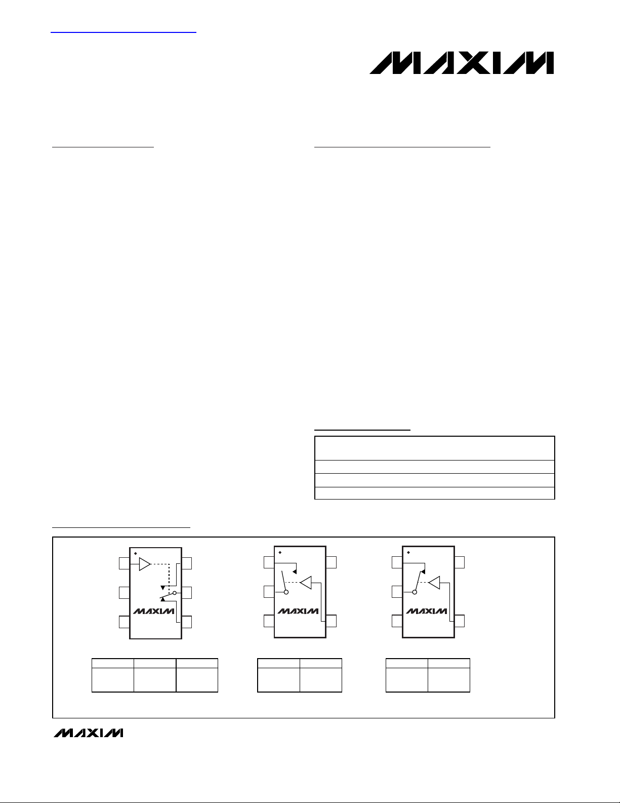
Pin Configurations/Functional Diagrams/Truth Tables
19-1714; Rev 0; 4/00
For free samples and the latest literature, visit www.maxim-ic.com or phone 1-800-998-8800.
For small orders, phone 1-800-835-8769.
Ordering Information
Rail-to-Rail is a registered trademark of Nippon Motorola, Ltd.
查询MAX4561EUT-T供应商查询MAX4561EUT-T供应商
TEMP.
PART
MAX4561EUT-T -40°C to +85°C 6 SOT23 AAIE
MAX4568EUK-T -40°C to +85°C 5 SOT23 ADOE
MAX4569EUK-T -40°C to +85°C 5 SOT23 ADOF
RANGE
PACKAGE
PIN-
SOT
TOP M ARK
TOP VIEW
16NO
IN
V+
2
MAX4561
34
SOT23-6
LOGIC NO
0
1
OFF
ON
5 COM
NCGND
NC
ON
OFF
15V+COM
2
NO
MAX4568
34
SOT23-5
LOGIC SWITCH
0
1
SWITCHES SHOWN FOR LOGIC "0" INPUT.
INGND
OFF
ON
15V+COM
2
NC
MAX4569
34
SOT23-5
LOGIC SWITCH
0
1
INGND
ON
OFF
Page 2
MAX4561/MAX4568/MAX4569
±15kV ESD-Protected, Low-Voltage,
SPDT/SPST, CMOS Analog Switches
2 _______________________________________________________________________________________
ABSOLUTE MAXIMUM RATINGS
ELECTRICAL CHARACTERISTICS—Single +5V Supply
(V+ = +4.5V to +5.5V, VIH= +2.4V, VIL= +0.8V, TA= T
MIN
to T
MAX
, unless otherwise specified. Typical values are at TA= +25°C.)
(Notes 2, 3)
Stresses beyond those listed under “Absolute Maximum Ratings” may cause permanent damage to the device. These are stress ratings only, and functional
operation of the device at these or any other conditions beyond those indicated in the operational sections of the specifications is not implied. Exposure to
absolute maximum rating conditions for extended periods may affect device reliability.
V+ to GND ................................................................-0.3 to +13V
IN, COM, NO, NC to GND (Note 1) ..............-0.3V to (V+ + 0.3V)
Continuous Current (any terminal)....................................±10mA
Peak Current
(NO, NC, COM; pulsed at 1ms 10% duty cycle).........±30mA
ESD Protection per Method IEC 1000-4-2 (NO, NC)
Air-Gap Discharge ........................................................±15kV
Contact Discharge ..........................................................±8kV
ESD Protection per Method 3015.7
V+, GND, IN, COM.......................................................±2.5kV
NO, NC..........................................................................±15kV
Continuous Power Dissipation (T
A
= +70°C)
SOT23 (derate 8.7mW/°C above +70°C)....................696mW
Operating Temperature Range ...........................-40°C to +85°C
Storage Temperature Range .............................-65°C to +150°C
Lead Temperature (soldering, 10s) .................................+300°C
Note 1: Signals on NO, NC, COM, or IN exceeding V+ or GND are clamped by internal diodes. Limit forward current to maximum
current rating.
PARAMETER
SYMBOL
CONDITIONS
MIN
TYP
MAX
UNITS
ANALOG SWITCH
Input Voltage Range
V
COM
,
0V+V
TA = +25°C4570
On-Resistance R
ON
V+ = 4.5V, I
COM
= 1mA;
V
NO
or VNC = 1V, 3.5V
T
A
= T
MIN
to T
MAX
75
Ω
TA = +25°C0.52
On-Resistance Match
Between Channels
(Note 4)
∆R
ON
V+ = 4.5V, I
COM
=1mA;
V
NO
or VNC = 1V, 3.5V
T
A
= T
MIN
to T
MAX
3
Ω
TA = +25°C24
On-Resistance Flatness
(Note 5)
)
V+ = 4.5V, I
COM
= 1mA;
V
NO
or VNC = 1V, 2.25V, 3.5V
T
A
= T
MIN
to T
MAX
5
Ω
TA = +25°C
0.5
Off-Leakage Current
(NO or NC)
I
NO(OFF)
,
)
V+ = 5.5V, V
COM
= 1V, 4.5V;
V
NO
or VNC = 4.5V, 1V
T
A
= T
MIN
to T
MAX
-5 5
nA
TA = +25°C
0.5
COM Off-Leakage Current
(MAX4568/MAX4569 only)
)
V+ = 5.5V, V
COM
= 1V, 4.5V;
V
NO
or VNC = 4.5V, 1V
T
A
= T
MIN
to T
MAX
-5 5
nA
TA = +25°C-1 1
COM On-Leakage Current
)
V+ = 5.5V, V
COM
= 1V, 4.5V;
V
NO
or VNC = 1V, 4.5V or
floating
T
A
= T
MIN
to T
MAX
-10 10
nA
LOGIC INPUT
Input Logic High V
IH
2.4 V
Input Logic Low V
IL
0.8 V
Input Leakage Current I
IN
VIN = 0 or V+ -1 1 µA
VNO, V
NC
R
FLAT(ON
-0.5 0.01
-0.5 0.01
I
NC(OFF
I
COM(OFF
ICOM(ON
Page 3
MAX4561/MAX4568/MAX4569
±15kV ESD-Protected, Low-Voltage,
SPDT/SPST, CMOS Analog Switches
_______________________________________________________________________________________ 3
ELECTRICAL CHARACTERISTICS—Single +5V Supply (continued)
(V+ = +4.5V to +5.5V, VIH= +2.4V, VIL= +0.8V, TA= T
MIN
to T
MAX
, unless otherwise specified. Typical values are at TA= +25°C.)
(Notes 2, 3)
PARAMETER
SYMBOL
CONDITIONS
MIN
TYP
MAX
UNITS
SWITCH DYNAMIC CHARACTERISTICS
TA = +25°C
90
150
Turn-On Time t
ON
V
N O
, V
N C
= 3V , RL = 300Ω ,
C
L
= 35p F; Fi gur e 1
T
A
= T
MIN
to T
MAX
180
ns
TA = +25°C4080
Turn-Off Time t
OFF
V
N O
, V
N C
= 3V , RL = 300Ω ,
C
L
= 35p F, Fi gur e 1
T
A
= T
MIN
to T
MAX
100
ns
Break-Before-Make Delay
(MAX4561 only)
t
BBM
VNO, VNC = 3V, RL =
550 ns
MAX4561 17
Charge Injection Q
V
GEN
= 2V, CL = 1.0nF,
R
GEN
= 0; Figure 3
T
A
=
6
pC
NO or NC Off
Capacitance
C
OFF
VNO = VNC = GND,
f = 1MHz, Figure 4
T
A
= +25°C20pF
COM Off-Capacitance
(MAX4568/MAX4569 only)
C
COM
Figure 4
T
A
= +25°C12pF
MAX4561 31
COM On-Capacitance C
COM
V
COM
= VNO, VNC = GND,
f = 1MHz, Figure 4
TA =
20
pF
Off-Isolation (Note 6)
V
ISO
VNO = VNC = 1V
RMS
,
R
L
= 50Ω; CL = 5pF,
f = 1MHz; Figure 5
T
A
= +25°C -75 dB
Total Harmonic Distortion THD
R
L
= 600Ω, 5Vp-p,
f = 20Hz to 20kHz
T
A
= +25°C
%
TA = +25°C
mA
ESD SCR Holding Current
I
H
TA = +85°C70
POWER SUPPLY
Power-Supply Range V+ 1.8 12 V
TA = +25°C
1
Positive Supply Current I+ V+ = 5.5V, VIN = 0 or V+
T
A
= T
MIN
to T
MAX
10
µA
300Ω, CL = 35pF, Figure 2
V
COM
= GND, f = 1MHz,
+25°C
+25°C
M AX 4568/9
M AX 4568/9
0.01
110
0.05
Page 4
0
50
150
100
200
250
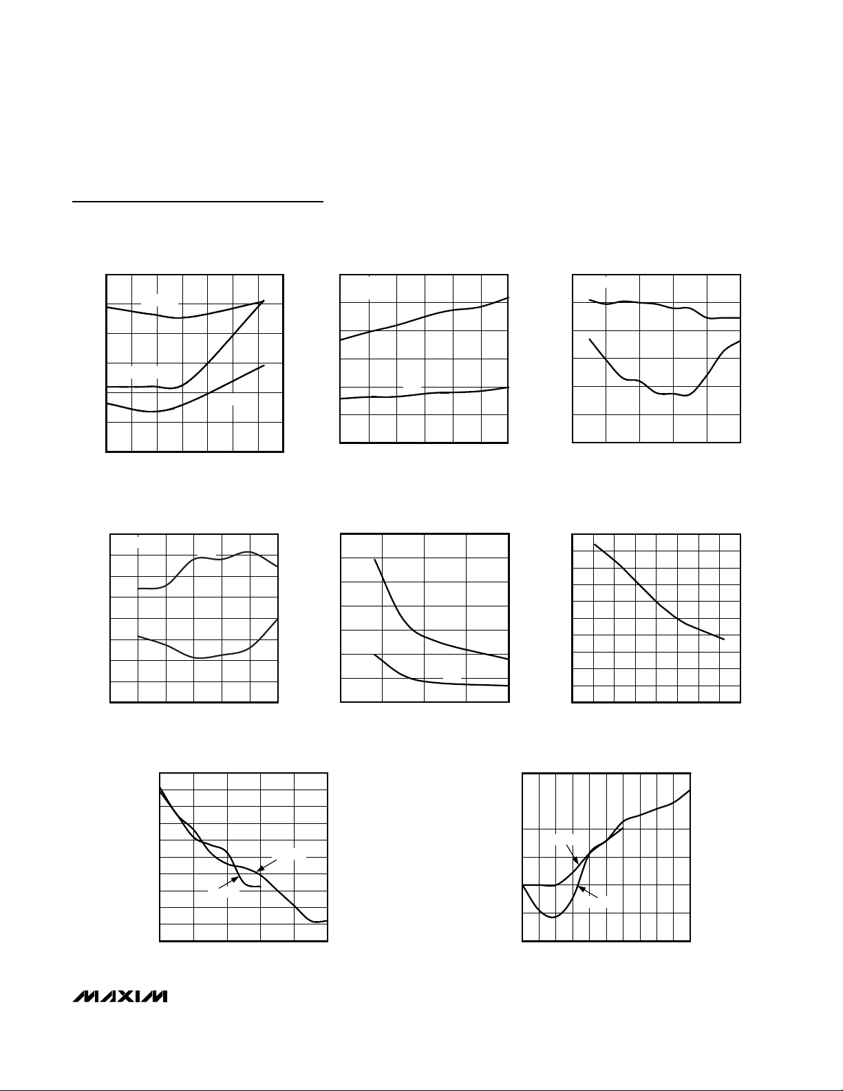
ON-RESISTANCE
vs. V
COM
AND SUPPLY VOLTAGE
MAX4561/8/9-01
V
COM
(V)
R
ON
(Ω)
04
8
12
V+ = +1.8V
V+ = +2.5V
V+ = +3.3V
V+ = +5V
V+ = +9V
V+ = +12V
0
30
20
10
40
50
60
021 345
ON-RESISTANCE
vs. TEMPERATURE
MAX4561/8/9-02
V
COM
(V)
R
DS(ON)
(Ω)
V+ = 5V
TA = +85°C
TA = +25°C
TA = -40°C
0
400
200
1000
800
600
1600
1400
1200
1800
-40 0 20-20 40 60 80 100
LEAKAGE CURRENT
vs. TEMPERATURE
MAX4561/8/9 TOC3
TEMPERATURE (°C)
LEAKAGE CURRENT (pA)
OFF
ON
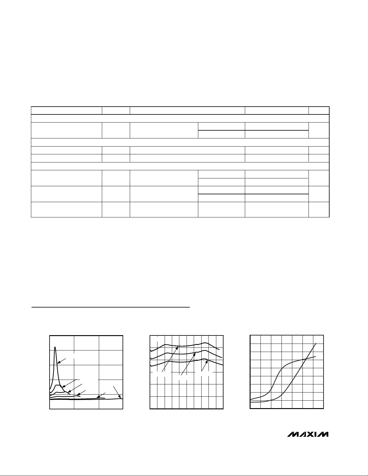
Typical Operating Characteristics
(TA = +25°C, unless otherwise noted.)
MAX4561/MAX4568/MAX4569
±15kV ESD-Protected, Low-Voltage,
SPDT/SPST, CMOS Analog Switches
4 _______________________________________________________________________________________
ELECTRICAL CHARACTERISTICS—Single +3V Supply
(V+ = +2.7V to +3.6V, VIH= +2.0V, VIL= +0.6V, TA= T
MIN
to T
MAX
, unless otherwise specified. Typical values are at TA= +25°C.)
(Notes 2, 3)
Note 2: The algebraic convention, where the most negative value is a minimum and the most positive value is a maximum, is used
in this data sheet.
Note 3: Parameters are 100% tested at +25°C and guaranteed by correlation at the full rated temperature.
Note 4: ∆R
ON
= R
ON(MAX)
- R
ON(MIN)
.
Note 5: Flatness is defined as the difference between the maximum and the minimum value of on-resistance as measured over the
specified analog signal ranges.
Note 6: Off-Isolation = 20log
10
(V
COM/VNO
), V
COM
= output, VNO= input to off switch.
PARAMETER
SYMBOL
CONDITIONS
MIN
TYP
MAX
UNITS
ANALOG SWITCH
TA = +25°C75120
On-Resistance R
ON
I
COM
= 1mA, VNO or
V
NC
= 1.5V, V+ = 2.7V
150
Ω
LOGIC INPUT
Input Logic High V
IH
2.0 V
Input Logic Low V
IL
0.6 V
SWITCH DYNAMIC CHARACTERISTICS
TA = +25°C
250
Turn-On Time t
ON
V
N O
or V
N C
= 1.5V, RL = 300Ω,
C
L
= 35pF, Figure 1
300
ns
TA = +25°C 60 100
Turn-Off Time t
OFF
V
N O
or V
N C
= 1.5V, RL = 300Ω,
C
L
= 35pF, Figure 1
150
ns
Break-Before-Make Delay
(MAX4561 only)
T
BBM
CL = 35pF, Figure 2
T
A
= +25°C
1.5 80
ns
TA = T
MIN
to T
MAX
150
TA = T
TA = T
MIN
MIN
to T
to T
MAX
MAX
VNO or VNC = 3V, RL = 300Ω,
Page 5
MAX4561/MAX4568/MAX4569
±15kV ESD-Protected, Low-Voltage,
SPDT/SPST, CMOS Analog Switches
________________________________________________________________________________________ 5
Typical Operating Characteristics (continued)
(TA= +25°C, unless otherwise noted.)
0
40
20
80
60
120
100
140
180
160
200
-60 -20 0-40 20 40 60 80 100
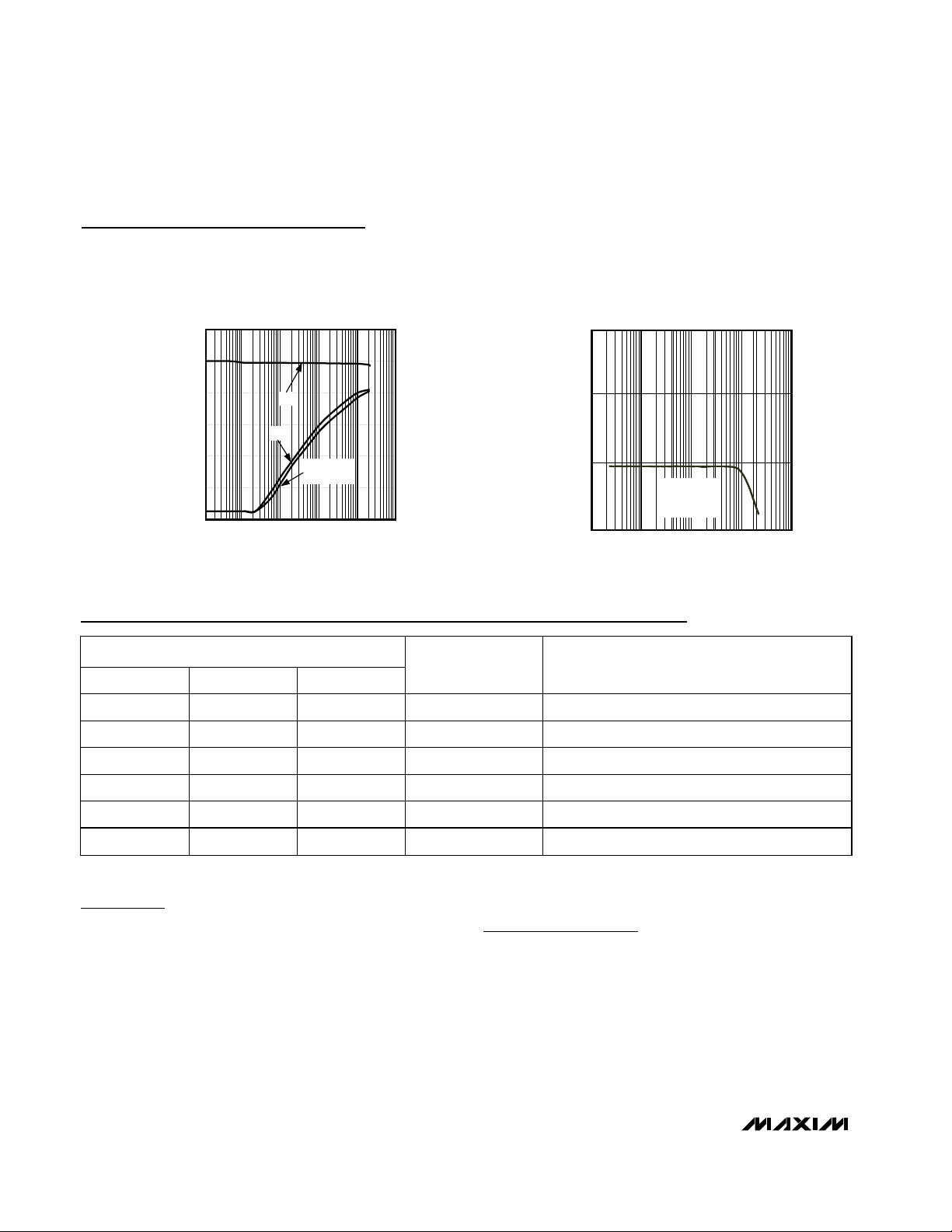
SCR HOLDING CURRENT
vs. TEMPERATURE
MAX4561/8/9-08
TEMPERATURE (°C)
HOLDING CURRENT (mA)
I
H
-40
-25
-30
-35
-20
-15
-10
-5
0
5
10
021 345
MAX4561
CHARGE INJECTION vs. V
COM
MAX4561/8/9-09a
V
COM
(V)
Q (pC)
V+ = 3V
V+ = 5V
-10
5
0
-5
10
15
20
021 345
MAX4568/MAX4569
CHARGE INJECTION vs. V
COM
MAX4561/8/9-09b
V
COM
(V)
Q (pC)
V+ = 5V
V+ = 3V
SUPPLY CURRENT
vs. TEMPERATURE AND SUPPLY VOLTAGE
60
50
40
30
20
SUPPLY CURRENT (nA)
10
0
-40 20 40-20 0 60 80 100
160
140
120
100
(ns)
OFF
80
/t
ON
t
60
40
20
0
V+ = 12V
V+ = 3V
V+ = 5V
TEMPERATURE (°C)
TURN-ON/TURN-OFF TIME vs. V
V+ = 3V
0 1.00.5 1.5 2.0 2.5 3.0
t
ON
t
OFF
V
(V)
COM
COM
MAX4561/8/9-04
MAX4561/8/9-06b
TURN-ON/TURN-OFF TIME
vs. TEMPERATURE
120
V+ = 5V
= 3V
V
COM
100
80
(ns)
OFF
60
/t
ON
t
40
20
0
-40 0 20-20 40 60 80
t
ON
t
OFF
TEMPERATURE (°C)
TURN-ON/TURN-OFF TIME
vs. SUPPLY VOLTAGE
350
300
250
200
(ns)
OFF
/t
150
ON
t
100
50
0
12345
SUPPLY VOLTAGE (V)
t
ON
t
OFF
MAX4561/8/9-05
MAX4561/8/9-07
TURN-ON/TURN-OFF TIME vs. V
120
V+ = 5V
100
80
(ns)
OFF
60
/t
ON
t
40
20
0
021 345
t
ON
t
OFF
V
(V)
COM
COM
MAX4561/8/9-06a
Page 6
MAX4561/MAX4568/MAX4569
±15kV ESD-Protected, Low-Voltage,
SPDT/SPST, CMOS Analog Switches
6 _______________________________________________________________________________________
Applications Information
Do not exceed the absolute maximum ratings because
stresses beyond the listed ratings may cause permanent damage to the device.
Proper power-supply sequencing is recommended for
all CMOS devices. Always sequence V+ on first, followed by the logic inputs, NO/NC, or COM.
Operating Considerations for
High-Voltage Supply
The MAX4561/MAX4568/MAX4569 are capable of
+12V single-supply operation with some precautions.
The absolute maximum rating for V+ is +13V (referenced to GND). When operating near this region,
bypass V+ with a 0.1µF min capacitor to ground as
close to the device as possible.
Typical Operating Characteristics (continued)
(TA= +25°C, unless otherwise noted.)
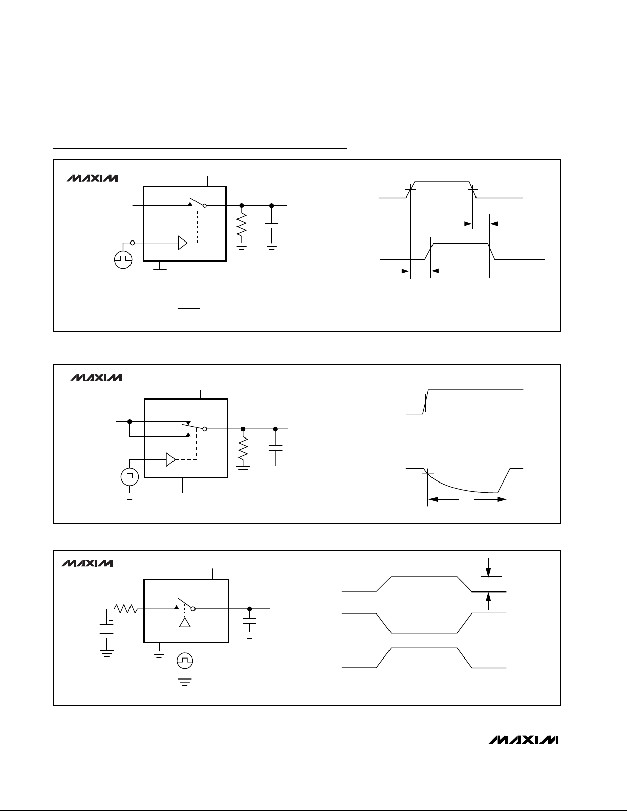
10 1000100 10,000 100,000
TOTAL HARMONIC DISTORTION
vs. FREQUENCY
MAX4561/8/9-11
FREQUENCY (Hz)
THD (%)
1
0.001
0.01
0.1
600Ω IN and
OUT
V+ = 5V
Pin Description
PIN
MAX4561 MAX4568 MAX4569
NAME FUNCTION
1 4 4 IN Logic Control Input
2 5 5 V+ Positive Supply Voltage
3 3 3 GND Ground
4 – 2 NC Analog Switch Normally Closed Terminal
5 1 1 COM Analog Switch Common Terminal
62– NO
Analog Switch Normally Open Terminal
0.01 0.1
100 1000
FREQUENCY RESPONSE
MAX4561/8/9-10
FREQUENCY (MHz)
LOSS (dB)
20
-100
-80
-60
-40
-20
0
110
ON
OFF
CROSSTALK
MAX4561
Page 7

MAX4561/MAX4568/MAX4569
±15kV ESD-Protected, Low-Voltage,
SPDT/SPST, CMOS Analog Switches
_______________________________________________________________________________________ 7
±15kV ESD Protection
The MAX4561/MAX4568/MAX4569 are ±15kV ESD-protected at the NC/NO terminals in accordance with
IEC1000-4-2. To accomplish this, bidirectional SCRs
are included on-chip between these terminals. When
the voltages at these terminals go Beyond-the-Rails™,
the corresponding SCR turns on in a few nanoseconds
and bypasses the surge safely to ground. This method
is superior to using diode clamps to the supplies
because unless the supplies are very carefully decoupled through low-ESR capacitors, the ESD current
through the diode clamp could cause a significant
spike in the supplies. This may damage or compromise
the reliability of any other chip powered by those same
supplies.
There are diodes from NC/NO to the supplies in addition to the SCRs. A resistance in series with each of
these diodes limits the current into the supplies during
an ESD strike. The diodes protect these terminals from
overvoltages that are not a result of ESD strikes. These
diodes also protect the device from improper powersupply sequencing.
Once the SCR turns on because of an ESD strike, it
remains on until the current through it falls below its
“holding current.” The holding current is typically
110mA in the positive direction (current flowing into
the NC/NO terminal) at room temperature (see
SCR Holding Current vs.Temperature in the Typical
Operating Characteristics). Design the system so that
any sources connected to NC/NO are current-limited to
a value below the holding current to ensure the SCR
turns off when the ESD event is finished and normal
operation resumes. Also, remember that the holding
current varies significantly with temperature. The worst
case is at +85°C when the holding currents drop to
70mA. Since this is a typical number to guarantee turnoff of the SCRs under all conditions, the sources connected to these terminals should be current-limited to
no more than half this value. When the SCR is latched,
the voltage across it is approximately 3V. The supply
voltages do not affect the holding current appreciably.
The sources connected to the COM side of the switches
need not be current limited since the switches turn off
internally when the corresponding SCR(s) latch.
Even though most of the ESD current flows to GND
through the SCRs, a small portion of it goes into V+.
Therefore, it is a good idea to bypass the V+ with 0.1µF
capacitors directly to the ground plane.
ESD protection can be tested in various ways. Inputs
are characterized for protection to the following:
•±15kV using the Human Body Model
•±8kV using the Contact Discharge method speci-
fied in IEC 1000-4-2 (formerly IEC 801-2)
•±15kV using the Air-Gap Discharge method specified in IEC 1000-4-2 (formerly IEC 801-2)
ESD Test Conditions
Contact Maxim Integrated Products for a reliability report
that documents test setup, methodology, and results.
Human Body Model
Figure 6 shows the Human Body Model, and Figure 7
shows the waveform it generates when discharged into a
low impedance. This model consists of a 100pF capacitor
charged to the ESD voltage of interest, which can be discharged into the test device through a 1.5kΩ resistor.
IEC 1000-4-2
The IEC 1000-4-2 standard covers ESD testing and
performance of finished equipment; it does not specifically refer to integrated circuits. The MAX4561 enables
the design of equipment that meets Level 4 (the highest
level) of IEC 1000-4-2, without additional ESD protection components.
The major difference between tests done using the
Human Body Model and IEC 1000-4-2 is higher peak current in IEC 1000-4-2. Because series resistance is lower
in the IEC 1000-4-2 ESD test model (Figure 8), the ESD
withstand voltage measured to this standard is generally
lower than that measured using the Human Body Model.
Figure 9 shows the current waveform for the ±8kV IEC
1000-4-2 Level 4 ESD Contact Discharge test.
The Air-Gap test involves approaching the device with a
charged probe. The Contact Discharge method connects
the probe to the device before the probe is energized.
Chip Information
PROCESS: CMOS
Beyond-the-Rails is a trademark of Maxim Integrated Products.
TRANSISTOR COUNT: 69 (MAX4561)
39 (MAX4568/MAX4569)
Page 8
MAX4561/MAX4568/MAX4569
±15kV ESD-Protected, Low-Voltage,
SPDT/SPST, CMOS Analog Switches
8 _______________________________________________________________________________________
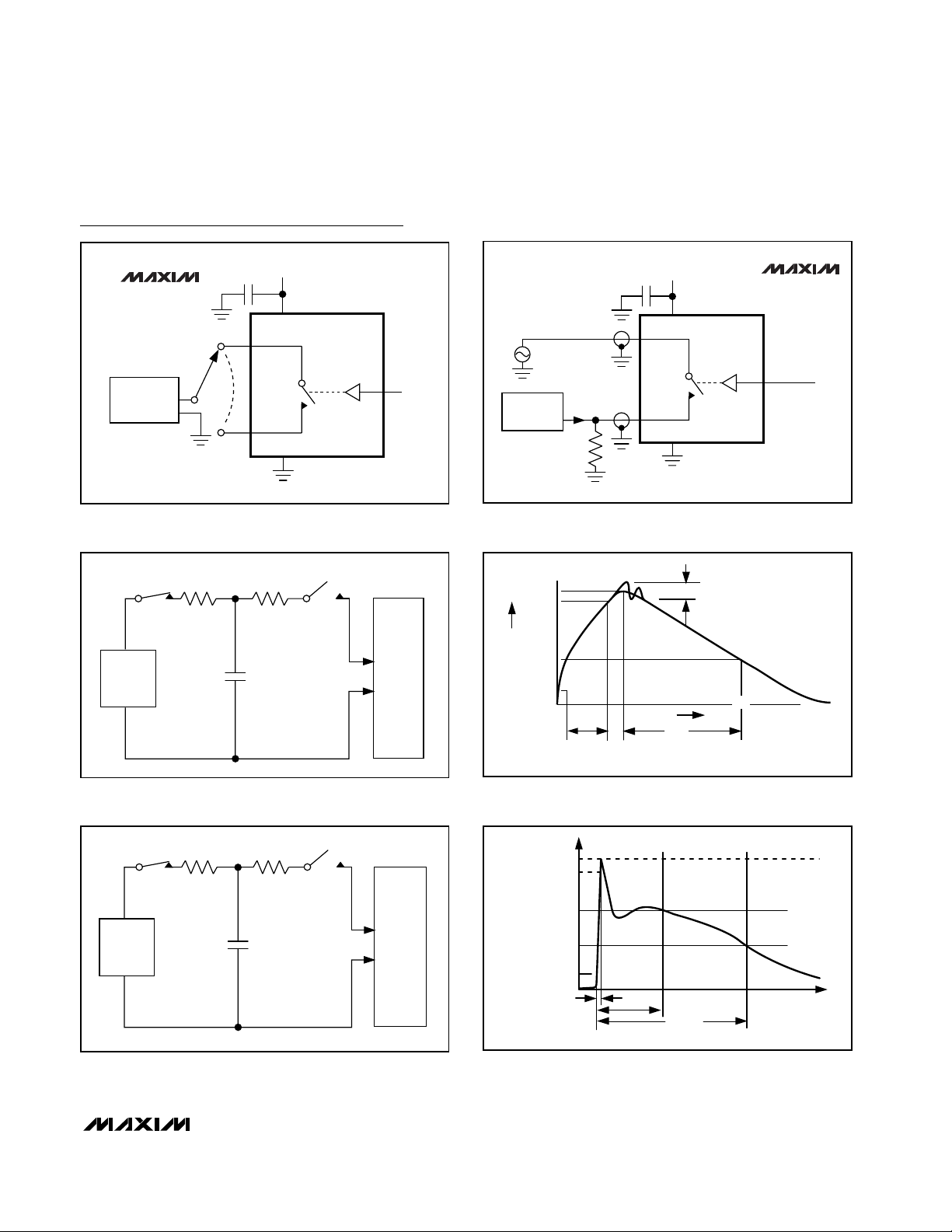
Figure 1. Switching Time
Figure 2. Break-Before-Make Interval
Figure 3. Charge Injection
Test Circuits/Timing Diagrams
MAX4561
MAX4568
MAX4569
LOGIC
INPUT
SWITCH
INPUT
C
V
RL + R
V+
V+
NO
OR NC
IN
GND
INCLUDES FIXTURE AND STRAY CAPACITANCE.
L
OUT
= V
COM (
R
COM
R
L
L
)
ON
SWITCH
OUTPUT
V
OUT
C
L
OUTPUT
LOGIC
INPUT
SWITCH
+3V
0
0
50%
V
OUT
t
ON
LOGIC INPUT WAVEFORMS INVERTED FOR SWITCHES
THAT HAVE THE OPPOSITE LOGIC SENSE.
0.9 x V
0UT
tr < 20ns
tf < 20ns
t
OFF
0.9 x V
OUT
GND
V+
V+
V
COM
OUT
R
L
C
L
MAX4561
+3V
LOGIC
INPUT
NC
NO
IN
C
INCLUDES FIXTURE AND STRAY CAPACITANCE.
L
MAX4561
V+
MAX4568
MAX4569
V
GEN
R
GEN
NC
OR NO
GND
IN
= LOGIC INPUT
V
IN
V+
COM
V
OUT
V
OUT
C
L
+3V
0
IN
+3V
0
+3V
LOGIC
INPUT
SWITCH
OUTPUT
(V
0
)
OUT
Q = (∆V
IN DEPENDS ON SWITCH CONFIGURATION;
INPUT POLARITY DETERMINED BY SENSE OF SWITCH.
OUT
50%
0.9 x V
)(CL)
OUT
t
BBM
∆V
OUT
0.9 x V
OUT
Page 9
MAX4561/MAX4568/MAX4569
±15kV ESD-Protected, Low-Voltage,
SPDT/SPST, CMOS Analog Switches
_______________________________________________________________________________________ 9
Figure 4. Channel On/Off-Capacitance
Figure 5. Off-Isolation/On-Channel
Figure 6. Human Body ESD Test Model
Figure 7. Human Body Model Current Waveform
Figure 8. IEC 1000-4-2 ESD Test Model
Figure 9. IED 1000-4-2 ESD Generator Current Waveform
Test Circuits/Timing Diagrams (continued)
V+
10nF
MAX4561
MAX4568
MAX4569
CAPACITANCE
METER
f = 1MHz
V+
COM
NC OR
NO
GND
R
D
1500Ω
DISCHARGE
RESISTANCE
STORAGE
CAPACITOR
HIGH-
VOLTAGE
DC
SOURCE
R
C
1M
CHARGE-CURRENT
LIMIT RESISTOR
C
s
100pF
V+
10nF
IN
DEVICE
UNDER
TEST
0 OR
3V
SIGNAL
GENERATOR 0dBm
ANALYZER
R
L
IP 100%
90%
AMPERES
36.8%
10%
0
0
t
RL
V+
COM
NC
OR NO
GND
I
r
TIME
t
DL
CURRENT WAVEFORM
IN
PEAK-TO-PEAK RINGING
(NOT DRAWN TO SCALE)
MAX4561
MAX4568
MAX4569
0 OR
3V
R
D
330Ω
DISCHARGE
RESISTANCE
STORAGE
CAPACITOR
HIGH-
VOLTAGE
DC
SOURCE
R
C
50M to 100M
CHARGE-CURRENT
LIMIT RESISTOR
C
s
150pF
DEVICE
UNDER
TEST
I
100%
90%
PEAK
I
10%
tr = 0.7ns to 1ns
30ns
60ns
t
Page 10

MAX4561/MAX4568/MAX4569
±15kV ESD-Protected, Low-Voltage,
SPDT/SPST, CMOS Analog Switches
10 ______________________________________________________________________________________
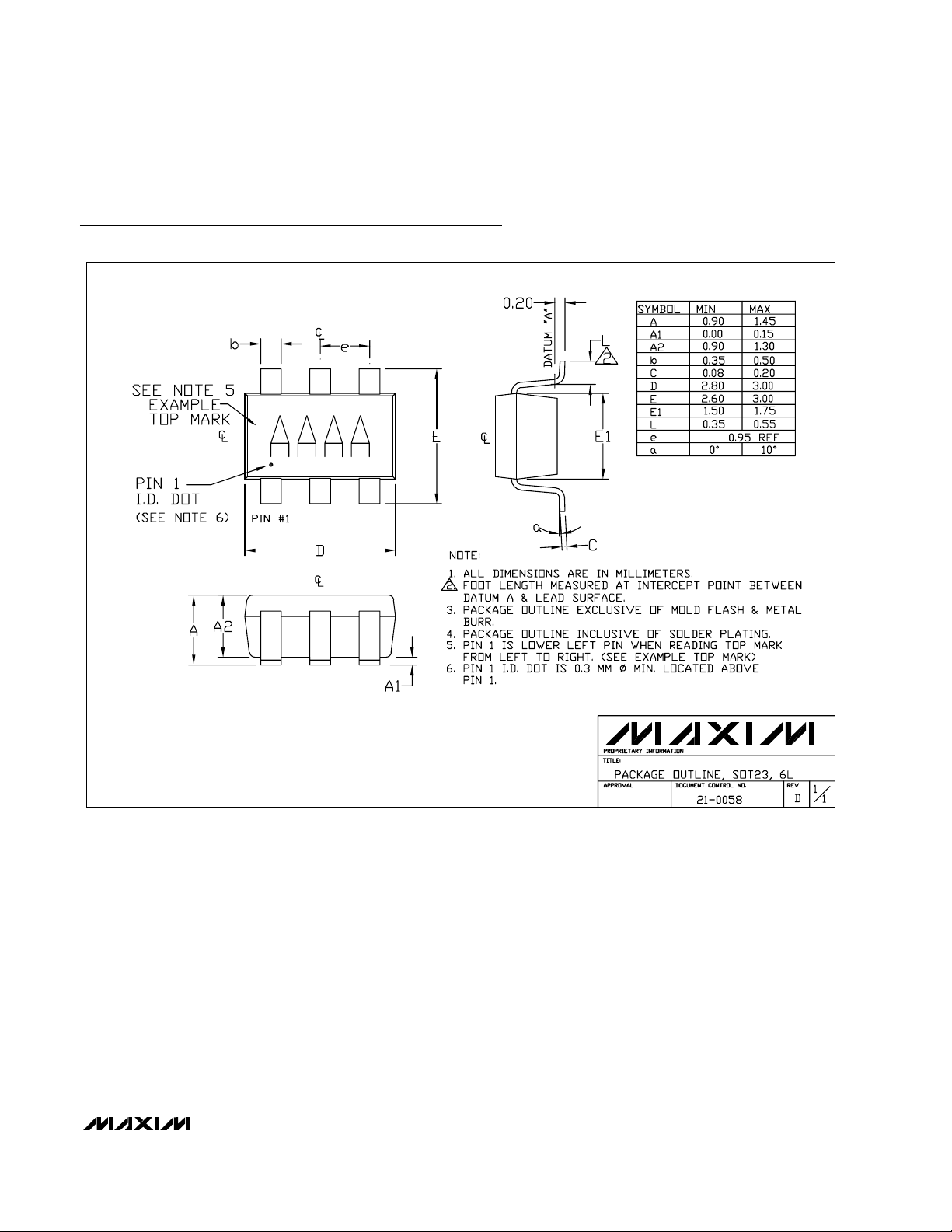
Package Information
SOT5L.EPS
Page 11
MAX4561/MAX4568/MAX4569
±15kV ESD-Protected, Low-Voltage,
SPDT/SPST, CMOS Analog Switches
______________________________________________________________________________________ 11
Package Information (continued)
6LSOT.EPS
Page 12

MAX4561/MAX4568/MAX4569
±15kV ESD-Protected, Low-Voltage,
SPDT/SPST, CMOS Analog Switches
Maxim cannot assume responsibility for use of any circuitry other than circuitry entirely embodied in a Maxim product. No circuit patent licenses are
implied. Maxim reserves the right to change the circuitry and specifications without notice at any time.
12 ____________________Maxim Integrated Products, 120 San Gabriel Drive, Sunnyvale, CA 94086 408-737-7600
© 2000 Maxim Integrated Products Printed USA is a registered trademark of Maxim Integrated Products.
NOTES
 Loading...