

Page 1
General Description
The MAX4564 is a low-voltage, dual-supply, singlepole/double-throw (SPDT) analog switch designed to
operate from dual ±1.8V to ±6V or single +1.8V to
+12V supplies. The low on-resistance (R
ON
= 40Ω at
±5V) and low power consumption (5µW) make this part
ideal for audio, video, and battery-powered applications. This switch offers low leakage currents (1nA
max) and fast switching speeds (tON= 60ns and t
OFF
= 40ns at ±5V, max).
The MAX4564 is available in 8-pin SOT23 and µMAX
packages.
________________________Applications
Battery-Operated Systems
Audio and Video Switching
Test Equipment
Communications Circuits
Sample-and-Hold Circuits
Communications Systems
Features
♦ 60Ω max (40Ω, typ) On-Resistance (RON)
♦ 3Ω max (0.75Ω, typ) R
ON
Matching Between
Channels
♦ 10Ω (max) R
ON
Flatness
♦ Low Charge Injection: 3pC (typ)
♦ Low ±1nA Leakage Current at +25°C
♦ Fast Switching
t
ON
= 60ns (max)
t
OFF
= 40ns (max)
♦ Guaranteed Break-Before-Make Switching
♦ TTL/CMOS-Logic Compatible
♦ Low Crosstalk: -72dB (1MHz)
♦ High Off-Isolation: -77dB (1MHz)
♦ Bandwidth -3dB: >450MHz (typ)
♦ Available in an 8-Pin SOT23 Package
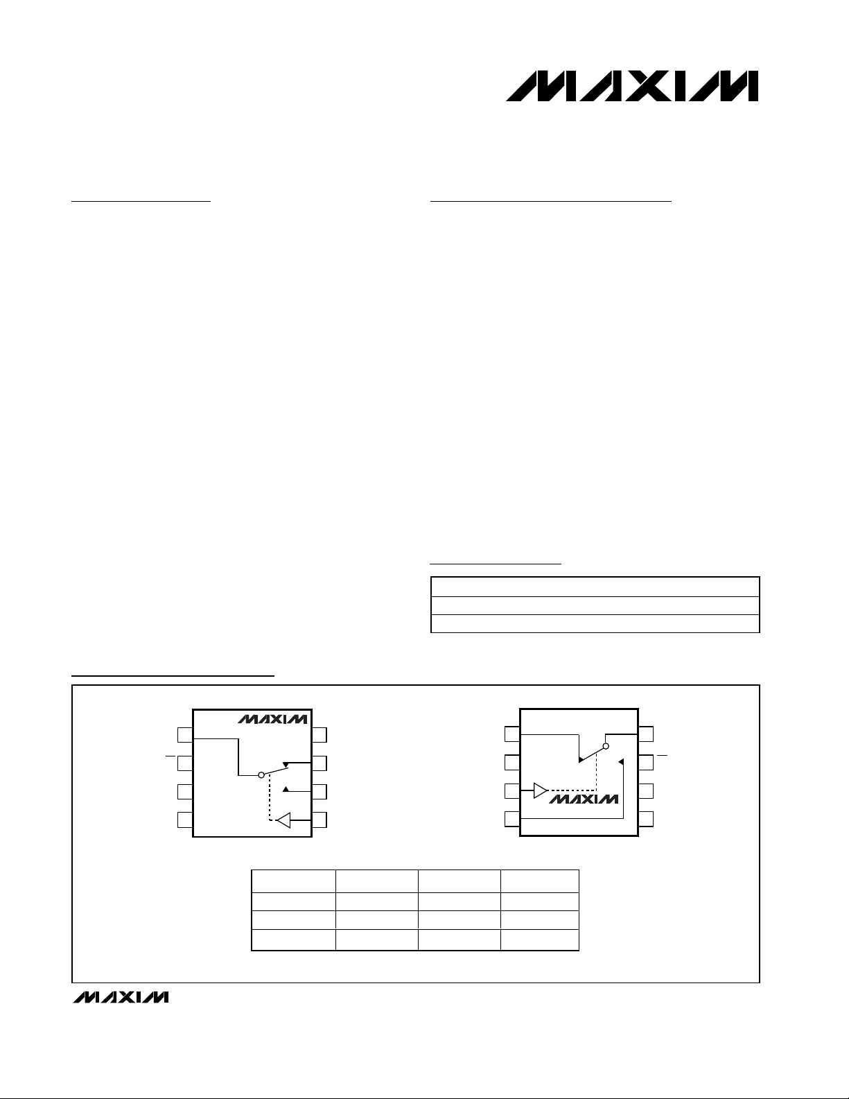
MAX4564
Low-Voltage, Dual-Supply,
SPDT Analog Switch with Enable
COM 1
2
3
4
8
7
6
5
EN
V-
GND
V+
NC
NO
IN
µMAX
MAX4564
Functional Diagrams/Pin Configurations/Truth Table
19-1765; Rev 1; 10/03
Ordering Information
NC 1
2
3
4
8
7
6
5
IN
NO
COM
V+
V-
GND
SOT23
MAX4564
EN
________________________________________________________________ Maxim Integrated Products 1
x = Don’t care
For pricing, delivery, and ordering information, please contact Maxim/Dallas Direct! at
1-888-629-4642, or visit Maxim’s website at www.maxim-ic.com.
PART TEMP RANGE PIN-PACKAGE
MAX4564EKA-T -40°C to +85°C 8 SOT23-8
MAX4564EUA
-40°C to +85°C
8 µMAX
EN IN NC NO
0 0 ON OFF
0 1 OFF ON
1 X OFF OFF
Page 2
Low-Voltage, Dual-Supply,
SPDT Analog Switch with Enable
ABSOLUTE MAXIMUM RATINGS
ELECTRICAL CHARACTERISTICS—±5V Supply
(V+ = +4.5V to +6V, V- = -4.5V to -6V, VIH= +2.4V, VIL= +0.8V, GND = 0, TA= T
MIN
to T
MAX
, unless otherwise noted. Typical values
are at T
A
= +25°C.) (Notes 2, 3)
Note 1: Signals on NO, NC, COM, IN, or EN exceeding V+ or V- are clamped by internal diodes. Limit forward-diode current to maximum
current rating.
Stresses beyond those listed under “Absolute Maximum Ratings” may cause permanent damage to the device. These are stress ratings only, and functional
operation of the device at these or any other conditions beyond those indicated in the operational sections of the specifications is not implied. Exposure to
absolute maximum rating conditions for extended periods may affect device reliability.
(Voltages Referenced to GND)
V+ ..........................................................................-0.3V to +13V
V- ...........................................................................-13V to +0.3V
V+ to V- ..................................................................-0.3V to +13V
EN, IN, COM, NC, NO (Note 1) .......... (V- - 0.3V) to (V+ + 0.3V)
Continuous Current (any terminal)................................... ±20mA
Peak Current, COM, NC, NO
(pulsed at 1ms, 10% duty cycle)................................ ±30mA
ESD per Method 3015.7...................................................... >2kV
Continuous Power Dissipation (T
A
= +70°C)
8-Pin SOT23 (derate 7.1mW/°C above +70°C) ..........571mW
8-Pin µMAX (derate 4.10mW/°C above +70°C) .........330mW
Operating Temperature Range
MAX4564E_A .................................................-40°C to +85°C
Junction Temperature .....................................................+150°C
Storage Temperature Range ............................-65°C to +150°C
Lead Temperature (soldering, 10s) ................................+300°C
)
)
)
)
)
MAX4564
2 _______________________________________________________________________________________
PARAMETER SYMBOL CONDITIONS T
ANALOG SWITCH
V
,
Analog Signal Range
On-Resistance R
On-Resistance Match Between
Channels (Note 4)
On-Resistance Flatness
(Note 5)
NO or NC Off-Leakage Current
COM
V
NO
∆R
R
FLAT(ON
I
NC(OFF
I
NO(OFF
, V
ON
NC
V+ = +4.5V, V- = -4.5V,
= 1mA; VNO, VNC = ±3.5V
I
COM
V+ = +4.5V, V- = -4.5V,
ON
= 1mA; VNO, VNC = ±3.5V
I
COM
V+ = +4.5V, V- = -4.5V, I
1mA; V
V+ = +5.5V, V- = -5.5V;
or
= +4.5V, -4.5V;
V
COM
V
, VNC = -4.5, +4.5V
NO
NO
, V
= -3.5V, 0, +3.5V
NC
COM
V+ = +5.5V, V- = -5.5V;
COM Off-Leakage Current I
COM On-Leakage Current
COM(OFF
I
COM(ON
V
= +4.5V, -4.5V;
COM
, VNC = -4.5, +4.5V
V
NO
V+ = +5.5V, V- = -5.5V, V
+4.5V, -4.5V; V
, VNC = +4.5V,
NO
COM
-4.5V, or floating
A
+25°C4060
E 100
+25°C 0.75 3
E4
=
+25°C 6.5 10
E13
+25°C -1 0.05 1
E-5 5
+25°C -1 0.05 1
E-5 5
=
+25°C -2 0.05 2
E -10 10
MIN TYP MAX UNITS
V- V+ V
Ω
Ω
Ω
nA
nA
nA
Page 3
MAX4564
Low-Voltage, Dual-Supply,
SPDT Analog Switch with Enable
ELECTRICAL CHARACTERISTICS—±5V Supply (continued)
(V+ = +4.5V to +6V, V- = -4.5V to -6V, VIH= +2.4V, VIL= +0.8V, GND = 0, TA= T
MIN
to T
MAX
, unless otherwise noted. Typical values
are at T
A
= +25°C.) (Notes 2, 3)
)
)
_______________________________________________________________________________________ 3
PARAMETER SYMBOL CONDITIONS T
SWITCH DYNAMIC CHARACTERISTICS
Turn-On Time t
Turn-Off Time t
ON
OFF
VNO, VNC = +3V, -3V,
= 1kΩ, CL = 35pF
R
L
VNO, VNC = +3V, -3V,
R
= 1kΩ, CL = 35pF
L
VNC = +3V, VNO = -3V,
Transition Time t
Break-Before-Make Time
(Note 6)
TRANS
t
BBM
Charge Injection Q
-3dB Bandwidth f
Off-Isolation (Note 7) V
-3dB
ISO
Crosstalk (Control Input to
Signal Output)
Crosstalk (Between Switches) V
CT
Total Harmonic Distortion THD
Control Input Capacitance C
NO or NC Off-Capacitance C
COM Off-Capacitance C
COM On-Capacitance
OFF
COM(OFF
C
COM(ON
V
= -3V, VNO = +3V,
NC
= 1kΩ, CL = 35pF
R
L
VNO, V
C
L
V
GEN
C
L
= +3V, -3V, RL = 300Ω,
NC
= 35pF
= 0, R
GEN
= 100pF
= 0,
RL = 50Ω, CL = 10pF,
= 1MHz
f
0dB
RL = 50Ω, CL = 10pF,
f
= 1MHz
IN
RL = 50Ω , C L = 10p F, V + = + 4.5V ,
V - = - 4.5V , f
= 1M H z, V EN = V
IN
RL = 50Ω, CL = 10pF,
f
= 1MHz
IN
R
= 600kΩ, CL = 50pF,
L
f
= 20kHz
IN
IN
fIN = 1MHz +25°C6 pF
fIN = 1MHz +25°C8 pF
fIN = 1MHz +25°C14 pF
LOGIC INPUT
Input Voltage Low V
Input Voltage High V
Input Leakage Current I
IL
IH
V+ = +5.5V, V- = -5.5V,
L
V
= V EN = 0 or +5.5V
IN
POWER SUPPLY
Power-Supply Range
Positive Supply Current I+
Negative Supply Current I-
V+ 2 6
V- -2
V+ = +5.5V, V- = -5.5V,
= V EN = 0 or +5.5V
V
IN
V+ = +5.5V, V- = -5.5V,
= V EN = 0 or +5.5V
V
IN
IH
+25°C4060
+25°C2840
+25°C5070
+25°C 5 15 ns
+25°C3 pC
+25°C 450 MHz
+25°C -77 dB
+25°C68 mV
+25°C -72 dB
+25°C 0.15 %
+25°C
+25°C -1 0.0001 1
+25°C -1 0.0001 1
MIN TYP MAX UNITS
A
E75
E50
E85
3pF
0.8 V
2.4 V
-1 0.0001 1
E -10 10
-6
E -10 10
E -10 10
ns
ns
ns
µA
V
µA
µA
Page 4
MAX4564
Low-Voltage, Dual-Supply,
SPDT Analog Switch with Enable
ELECTRICAL CHARACTERISTICS—Single +5V Supply
(V+ = +4.5V to +6V, V- = 0, VIH= +2.4V, VIL= +0.8V, GND = 0, TA= T
MIN
to T
MAX
, unless otherwise noted. Typical values are at
T
A
= +25°C.) (Notes 2, 3)
4 _______________________________________________________________________________________
PARAMETER SYMBOL CONDITIONS T
ANALOG SWITCH
V
,
Analog Signal Range
On-Resistance R
On-Resistance Match Between
Channels (Note 4)
SWITCH DYNAMIC CHARACTERISTICS
Turn-On Time t
Turn-Off Time t
Transition Time t
Break-Before-Make Time
(Note 6)
LOGIC INPUT
Input Voltage Low V
Input Voltage High V
Input Leakage Current I
POWER SUPPLY
Power-Supply Range V+ 1.8 12 V
Positive Supply Current I+
Negative Supply Current I-
V
NO
∆R
TRANS
COM
ON
ON
OFF
t
BBM
, V
NC
V+ = +4.5V, V- = 0,
I
COM
V+ = +4.5V, V- = 0,
ON
I
COM
VNO, VNC = +3V,
R
= 1kΩ, CL = 35pF
L
VNO, VNC = +3V,
R
= 1kΩ, CL = 35pF
L
VNC = +3V, VNO = 0,
V
NC
= 1kΩ, CL = 35pF
R
L
VNO, V
= 300Ω, CL = 35pF
R
L
IL
IH
V+ = +5.5V, V- = 0,
L
V
IN
V+ = +5.5V, V- = 0,
V
IN
V+ = +5.5V, V- = 0,
V
IN
= 1mA; VNO, VNC = +3.5 V
= 1mA; VNO, VNC = +3.5 V
= 0, VNO = +3V,
= +3V,
NC
= 0 or +5.5V
= V
EN
= V EN = 0 or +5.5V
= V EN = 0 or +5.5V
A
+25°C 72 100
E 125
+25°C 0.75 5
E7
+25°C6290
E 125
+25°C2260
E75
+25°C 68 100
E 130
E1035 ns
+25°C -1 0.0001 1
E -10 10
+25°C -1 0.0001 1
E -10 10
+25°C -1 0.0001 1
E -10 10
MIN TYP MAX UNITS
0V+V
0.8 V
2.4 V
Ω
Ω
ns
ns
ns
µA
µA
µA
Page 5

MAX4564
Low-Voltage, Dual-Supply,
SPDT Analog Switch with Enable
ELECTRICAL CHARACTERISTICS—Single +3V Supply
(V+ = +2.7V to +3.3V, V- = 0, VIH= +2.4V, VIL= +0.8V, GND = 0, TA= T
MIN
to T
MAX
, unless otherwise noted. Typical values are at
T
A
= +25°C.) (Notes 2, 3)
Note 2: The algebraic convention is used in this data sheet; the most negative value is shown in the minimum column.
Note 3: SOT-packaged products are 100% tested at +25°C and guaranteed by design at the full-rated temperature.
Note 4: ∆R
ON
= R
ON(MAX)
- R
ON(MIN).
Note 5: Flatness is defined as the difference between the maximum and minimum value of on-resistance as measured over the
specified analog signal ranges.
Note 6: Guaranteed by design.
Note 7: Off-Isolation = 20log
10
(V
COM
/ VNO), VNO= input to off switch.
_______________________________________________________________________________________ 5
ANALOG SWITCH
Analog Signal Range
On-Resistance R
On-Resistance Match Between
Channels (Note 4)
SWITCH DYNAMIC CHARACTERISTICS
Turn-On Time t
Turn-Off Time t
Break-Before-Make Time
(Note 6)
LOGIC INPUT
Input Voltage Low V
Input Voltage High V
Input Leakage Current I
PARAMETER SYMBOL CONDITIONS T
V
COM,
VNO, V
NC
V+ = +2.7V, V- = 0,
I
COM
V+ = +2.7V, V- = 0,
ON
I
COM
VNO, VNC = +1.5V,
R
VNO, VNC = +1.5V,
R
VNO, VNC = +1.5V,
R
IL
IH
V+ = +3.3V, V- = 0,
L
V
= 1mA; VNO, VNC = +1.5V
= 1mA; VNO, VNC = +1.5V
= 2kΩ, CL = 35pF
L
= 2kΩ, CL = 35pF
L
= 2kΩ, CL = 35pF
L
= V EN = 0 or +3.3V
IN
∆R
t
ON
ON
OFF
BBM
A
+25°C 160 275
E 300
+25°C 1.5 10
E12
+25°C 120 250
E 275
+25°C 40 110
E 125
E10 ns
+25°C -1 0.0001 1
E -10 10
MIN TYP MAX UNITS
0V+V
Ω
Ω
ns
ns
0.8 V
2.4 V
µA
Page 6

MAX4564
Low-Voltage, Dual-Supply,
SPDT Analog Switch with Enable
Typical Operating Characteristics
(TA = +25°C, unless otherwise noted.)
0
60
30
120
90
180
150
210
270
240
300
-5 -3 -2 -1-4 012 435
ON-RESISTANCE vs. V
COM
MAX4564 toc01
V
COM
(V)
R
ON
(Ω)
V+ = +1.8V,
V- = 0
V+ = +2.7V,
V- = 0
V+ = +4.5V,
V- = 0
V+ = +4.5V, V- = -4.5V
0
30
20
10
40
50
60
-5 -1-2-4-3 012345
ON-RESISTANCE vs. V
COM
AND TEMPERATURE (DUAL SUPPLIES)
MAX4564 toc02
V
COM
(V)
R
ON
(Ω)
V+ = +5V, V- = -5V
TA = +85°C
TA = + 25°C
TA = -40°C
0.01
0.1
1
10
100
1000
10,000
-40 -15 10 35 60 85
SWITCH LEAKAGE CURRENT
vs. TEMPERATURE
MAX4564 toc03
LEAKAGE CURRENT (pA)
V+ = +5V, V- = -5V
I
COM(ON)
I
COM(OFF),
I
NO(OFF),
I
NC(OFF)
TEMPERATURE (°C)
0
2
1
4
3
6
5
7
9
8
10
-5 -3 -2 -1-4 012 435
CHARGE INJECTION vs. V
COM
MAX4564 toc04
V
COM
(V)
Q (pC)
SINGLE
SUPPLY:
V+ = +5V,
V- = 0
DUAL SUPPLIES:
±5V
-3
-1
-2
1
0
2
I+
I-
3
-40 10-15 35 60 85
SUPPLY CURRENT vs. TEMPERATURE
MAX4564 toc05
TEMPERATURE (°C)
SUPPLY CURRENT (nA)
DUAL SUPPLIES:
V+ = +5V, V- = -5V, V
IN
= 0
0
0.01
0.03
0.02
0.04
0.05
042681012
SUPPLY CURRENT
vs. SUPPLY VOLTAGE
MAX4564 toc06
SUPPLY VOLTAGE (V)
SUPPLY CURRENT (nA)
V- = 0, VIN = 0
0.001
0.001
0.01
0.1
1
10
100
1000
012345
SUPPLY CURRENT
vs. LOGIC-LEVEL VOLTAGE
MAX4564 toc07
LOGIC-LEVEL VOLTAGE (V)
SUPPLY CURRENT (µA)
DUAL OR SINGLE
+5V SUPPLIES
SINGLE
SUPPLY:
V+ = +3V,
V- = 0
0
25
75
50
100
125
TURN-ON/TURN-OFF TIME
vs. SUPPLY VOLTAGE (DUAL SUPPLIES)
MAX4564 toc08
SUPPLY VOLTAGE (V)
t
ON
/t
OFF
(ns)
±2 ±4±3 ±5 ±6
t
ON
t
OFF
100
75
50
25
0
-40 10-15 35 60 85
TURN-ON/TURN-OFF TIME
vs. TEMPERATURE (DUAL SUPPLIES)
MAX4564 toc09
TEMPERATURE (°C)
t
ON
/t
OFF
(ns)
t
ON
t
OFF
V+ = +5V, V- = -5V
Typical Operating Characteristics
(TA = +25°C, unless otherwise noted.)
6 _______________________________________________________________________________________
Page 7

MAX4564
Low-Voltage, Dual-Supply,
SPDT Analog Switch with Enable
100
75
50
25
0
-40 10-15 35 60 85
TURN-ON/TURN-OFF TIME
vs. TEMPERATURE (SINGLE SUPPLY)
MAX4564 toc10
TEMPERATURE (°C)
t
ON
/t
OFF
(ns)
t
ON
t
OFF
V+ = +5V, V- = 0
-60
-50
-30
-40
-10
0
-20
10
0.1 1 10 100 1000
ON-RESPONSE, OFF-ISOLATION,
CROSSTALK vs. FREQUENCY
MAX4564 toc11
FREQUENCY (MHz)
LOSS (dB)
-70
-80
-90
-100
ON-RESPONSE
CROSSTALK
OFF-ISOLATION
V+ = +5V, V- = -5V
0.01
0.1
1
10
10 100 1k 10k 100k
TOTAL HARMONIC DISTORTION
vs. FREQUENCY
MAX4564 toc12
FREQUENCY (Hz)
THD (%)
V+ = +5V, V- = -5V
IN = OUT = 600Ω
0
0.25
0.50
0.75
1.00
1.25
1.50
1.75
2.00
2345
LOGIC-LEVEL THRESHOLD VOLTAGE
vs. SUPPLY VOLTAGE
MAX4564 toc13
SUPPLY VOLTAGE (V)
THRESHOLD VOLTAGE (V)
DUAL OR SINGLE SUPPLIES
Typical Operating Characteristics (continued)
(TA = +25°C, unless otherwise noted.)
_______________________________________________________________________________________ 7
Page 8

MAX4564
Low-Voltage, Dual-Supply,
SPDT Analog Switch with Enable
Detailed Description
The MAX4564 is a dual-supply SPDT CMOS analog
switch. The MAX4564 has break-before-make switching. The CMOS switch construction provides Rail-toRail®signal handling while consuming virtually no
power. Each of the two switches is independently controlled by a TTL/CMOS-level-compatible digital input.
Applications Information
Overvoltage Protection
Do not exceed the absolute maximum ratings because
stresses beyond the listed ratings may cause permanent damage to the device. Proper power-supply
sequencing is recommended for all CMOS devices.
Always sequence V+ on first, then V-, followed by the
logic inputs NO, NC, or COM. If power-supply
sequencing is not possible, add two small-signal
diodes (D1, D2) in series with supply pins. Adding
diodes reduces the analog signal range to one diode
drop below V+ and one diode drop above V-, but does
not affect the device’s low switch resistance and low
leakage characteristics.
Test Circuits/
Timing Diagrams
Pin Description
Figure 1. Overvoltage Protection Using Two External Blocking
Diodes
8 _______________________________________________________________________________________
Rail-to-Rail is a registered trademark of Nippon Motorola, Ltd.
µMAX
1 8 COM Analog Switch Common
27EN
3 6 V- Negative Supply Voltage
4 5 GND Ground
5 3 IN Digital Control Input
6 4 NO Analog Switch Normally Open
7 1 NC Analog Switch Normally Closed
8 2 V+ Positive Supply Voltage
SOT23 NAME FUNCTION
Device Enable. Drive EN low for normal SPDT switch operation. If EN is high, both
NO and NC are disconnected.
POSITIVE SUPPLY
D1
V+
MAX4564
V
g
NO
COM
V-
D2
NEGATIVE SUPPLY
Page 9

MAX4564
Low-Voltage, Dual-Supply,
SPDT Analog Switch with Enable
Figure 2. Switching Time
Figure 3. Break-Before-Make Interval
Figure 4. Charge Injection
Test Circuits/Timing Diagrams (continued)
_______________________________________________________________________________________ 9
MAX4564
V
IN
LOGIC
INPUT
C
L
MAX4564
V
N
LOGIC
INPUT
GND
V+
V+
COM
R
L
V+
V+
COM
R
L
V-
NO
OR NC
IN
GND
INCLUDES FIXTURE AND STRAY CAPACITANCE.
V-
NC
NO
IN
C
INCLUDES FIXTURE AND STRAY CAPACITANCE.
L
V
INH
LOGIC
INPUT
V
V
OUT
C
L
35pF
SWITCH
OUTPUT
V
OUT
C
L
35pF
INL
0
LOGIC
INPUT
V
OUT
50%
V
OUT
0.9 × V
0UT
t
ON
LOGIC INPUT WAVEFORMS INVERTED FOR SWITCHES
THAT HAVE THE OPPOSITE LOGIC SENSE.
V
INH
V
INL
50%
tr < 5ns
tf < 5ns
t
OFF
0.9 × V
OUT
0.9 × V
OUT
t
D
MAX4564
NC
OR NO
V
GEN
GND
V+V-
V+
COM
IN
TO V
V
IL
IH
V
OUT
C
L
V
OUT
IN
OFF
OFF
IN
IN DEPENDS ON SWITCH CONFIGURATION;
INPUT POLARITY DETERMINED BY SENSE OF SWITCH.
Q = (∆V
ON
ON
OUT
)(CL)
∆V
OUT
OFF
OFF
Page 10

MAX4564
Low-Voltage, Dual-Supply,
SPDT Analog Switch with Enable
Figure 5. On-Loss, Off-Isolation, and Crosstalk
Figure 6. Channel Off/On-Capacitance
Test Circuits/Timing Diagrams (continued)
Chip Information
TRANSISTOR COUNT: 116
PROCESS : CMOS
10 ______________________________________________________________________________________
10nF10nF
GND
V+
V
V+V-
COM
Rx
NO
IN
V
OUT
MEAS REF
NETWORK
ANALYZER
50Ω
50Ω 50Ω
50Ω
V-
0 OR V+
50Ω
IN
NC
MAX4564
V
OFF-ISOLATION = 20log
Rx = 50Ω
, VIN = DON'T CARE
EN = V
IH
ON-LOSS = 20log
(RON + 50) x 50
Rx =
+ 50) - 50
(R
ON
EN = V
, V
IL
IN = VIH, fOdB
CROSSTALK = 20log
(R
+ 50) x 50
ON
Rx =
+ 50) - 50
(R
ON
EN = VIL, V
IN = VIH
OUT
V
IN
V
OUT
V
AT f
IN
OdB
= 1MHz
V
OUT
V
IN
V+
10nF
V+
COM
CAPACITANCE
METER
f = 1MHz
NC or
NO
GND
MAX4564
V-
V
INL
IN
OR
V
INH
Page 11

MAX4564
Low-Voltage, Dual-Supply,
SPDT Analog Switch with Enable
______________________________________________________________________________________ 11
Package Information
(The package drawing(s) in this data sheet may not reflect the most current specifications. For the latest package outline information,
go to www.maxim-ic.com/packages
.)
b
C
L
PIN 1
I.D. DOT
(SEE NOTE 6)
A2
A
NOTE:
1. ALL DIMENSIONS ARE IN MILLIMETERS.
2. FOOT LENGTH MEASURED FROM LEAD TIP TO UPPER RADIUS OF
HEEL OF THE LEAD PARALLEL TO SEATING PLANE C.
3. PACKAGE OUTLINE EXCLUSIVE OF MOLD FLASH & METAL BURR.
4. PACKAGE OUTLINE INCLUSIVE OF SOLDER PLATING.
5. COPLANARITY 4 MILS. MAX.
6. PIN 1 I.D. DOT IS 0.3 MM ÿ MIN. LOCATED ABOVE PIN 1.
7. SOLDER THICKNESS MEASURED AT FLAT SECTION OF LEAD
BETWEEN 0.08mm AND 0.15mm FROM LEAD TIP.
8. MEETS JEDEC MO178.
SEE DETAIL "A"
C
L
e1
D
C
L
e
C
E
A1
L
C
SEATING PLANE C
E1
SYMBOL
A
C
L
L2
e
e1
0
L
DETAIL "A"
PROPRIETARY INFORMATION
TITLE:
L2
MIN
0.90
0.00A1
0.90A2
0.28b
0.09
2.80D
1.50E1
0.30
PACKAGE OUTLINE, SOT-23, 8L BODY
21-0078
0.25 BSC.
0.65 BSC.
1.95 REF.
0∞
GAUGE PLANE
0
MAX
1.45
0.15
1.30
0.45
0.20
3.00
3.002.60E
1.75
0.60
SOT23, 8L .EPS
8∞
REV.DOCUMENT CONTROL NO.APPROVAL
1
D
1
Page 12

MAX4564
Low-Voltage, Dual-Supply,
SPDT Analog Switch with Enable
Maxim cannot assume responsibility for use of any circuitry other than circuitry entirely embodied in a Maxim product. No circuit patent licenses are
implied. Maxim reserves the right to change the circuitry and specifications without notice at any time.
12 ____________________Maxim Integrated Products, 120 San Gabriel Drive, Sunnyvale, CA 94086 408-737-7600
© 2003 Maxim Integrated Products Printed USA is a registered trademark of Maxim Integrated Products.
Package Information (continued)
(The package drawing(s) in this data sheet may not reflect the most current specifications. For the latest package outline information,
go to www.maxim-ic.com/packages
.)
8
0.6±0.1
0.6±0.1
1
TOP VIEW
A2
e
FRONT VIEW
ÿ 0.50±0.1
D
b
E H
A1
4X S
BOTTOM VIEW
A
c
L
SIDE VIEW
8
1
DIM
A
A1
A2
b
c
D
e
E
H
L
α
S
INCHES
MIN
-
0.002
0.030
0.010
0.005
0.116
0.0256 BSC
0.116
0.188
0.016
0∞
0.0207 BSC
MAX
0.043
0.006
0.037
0.014
0.007
0.120
0.120
0.198
0.026
6∞
MILLIMETERS
MIN
0.05 0.15
0.25 0.36
0.13 0.18
2.95 3.05
2.95 3.05
4.78
0.41
MAX
-1.10
0.950.75
0.65 BSC
5.03
0.66
6∞0∞
0.5250 BSC
8LUMAXD.EPS
α
PROPRIETARY INFORMATION
TITLE:
PACKAGE OUTLINE, 8L uMAX/uSOP
REV.DOCUMENT CONTROL NO.APPROVAL
21-0036
1
J
1
 Loading...