

I2C is a trademark of Philips Corp.
SPI/QSPI are trademarks of Motorola, Inc.
MICROWIRE is a trademark of National Semiconductor Corp.
For free samples & the latest literature: http://www.maxim-ic.com, or phone 1-800-998-8800.
For small orders, phone 1-800-835-8769.
General Description
The MAX4562/MAX4563 serial-interface controlled
switches are ideal for multimedia applications. Each
device features 30Ω max on-resistance (RON), 5Ω R
ON
match, and 5Ω R
ON
flatness. Audio off-isolation and
crosstalk at 20kHz is -85dB, and video off-isolation and
crosstalk at 10MHz is -55dB. Both devices feature
“clickless” mode operation for audio applications.
The MAX4562/MAX4563 contain two normally open single-pole/double-throw (SPDT) switches and two normally open single-pole/single-throw (SPST) switches. The
MAX4562 features a 2-wire I2C™-compatible serial
interface. The MAX4563 features a 3-wire SPI™/QSPI™/
MICROWIRE™-compatible serial interface. Both parts
are available in 16-pin QSOP packages and operate
over the commercial and extended temperature
ranges.
Applications
Set-Top Boxes
PC Multimedia Boards
Audio Systems
Video Conferencing Systems
Features
♦ Selectable Soft-Switching Mode for “Clickless”
Audio Operation
♦ 30Ω max On-Resistance
♦ Audio Performance
-85dB Off-Isolation at 20kHz
-85dB Crosstalk at 20kHz
-0.007% THD
♦ Video Performance
-55dB Off-Isolation at 10MHz
-55dB Crosstalk at 10MHz
♦ T-Switch Configurable for Improved Off-Isolation
♦ Serial Interface
2-Wire I2C-Compatible (MAX4562)
3-Wire SPI/QSPI/MICROWIRE-Compatible
(MAX4563)
♦ Single-Supply Operation from +2.7V to +5.5V
MAX4562/MAX4563
Serially Controlled, Clickless
Audio/Video Switches
________________________________________________________________
Maxim Integrated Products
1
16
15
14
13
12
11
10
9
1
2
3
4
5
6
7
8
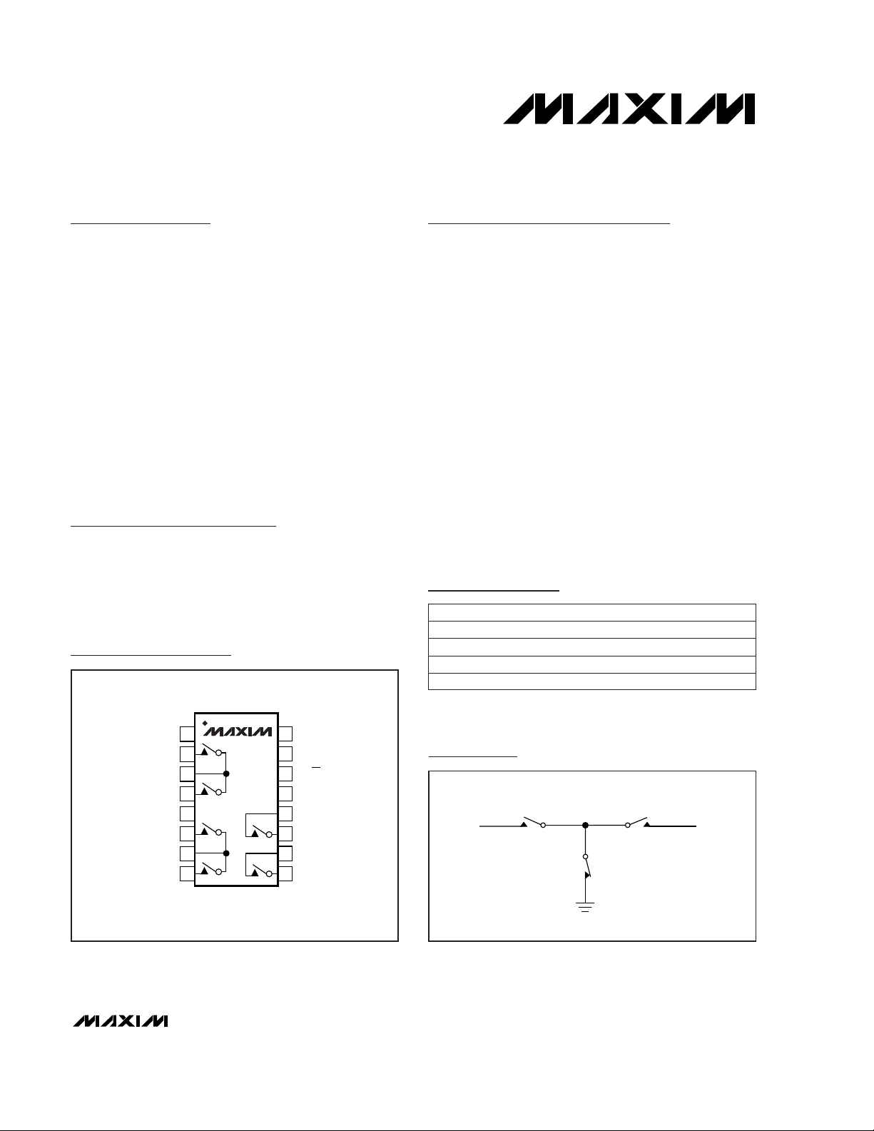
SCL (SCLK)
SDA (DIN)
A1 (DOUT)
COM4
( ) ARE FOR MAX4563
NO3
NO4
COM3NO2B
COM2
NO2A
GND
NO1B
COM1
NO1A
V+
QSOP
TOP VIEW
MAX4562
MAX4563
A0 (CS)
19-1461; Rev 0; 4/99
PART
MAX4562CEE
MAX4562EEE
MAX4563CEE
0°C to +70°C
-40°C to +85°C
0°C to +70°C
TEMP. RANGE PIN-PACKAGE
16 QSOP
16 QSOP
16 QSOP
Pin Configuration
Ordering Information
MAX4563EEE -40°C to +85°C 16 QSOP
Typical Operating Circuit
SIGNAL OUTSIGNAL IN
COM3
NO3
NO2B
NO2A
COM2
MAX4562/MAX4563
Serially Controlled, Clickless
Audio/Video Switches
2 _______________________________________________________________________________________
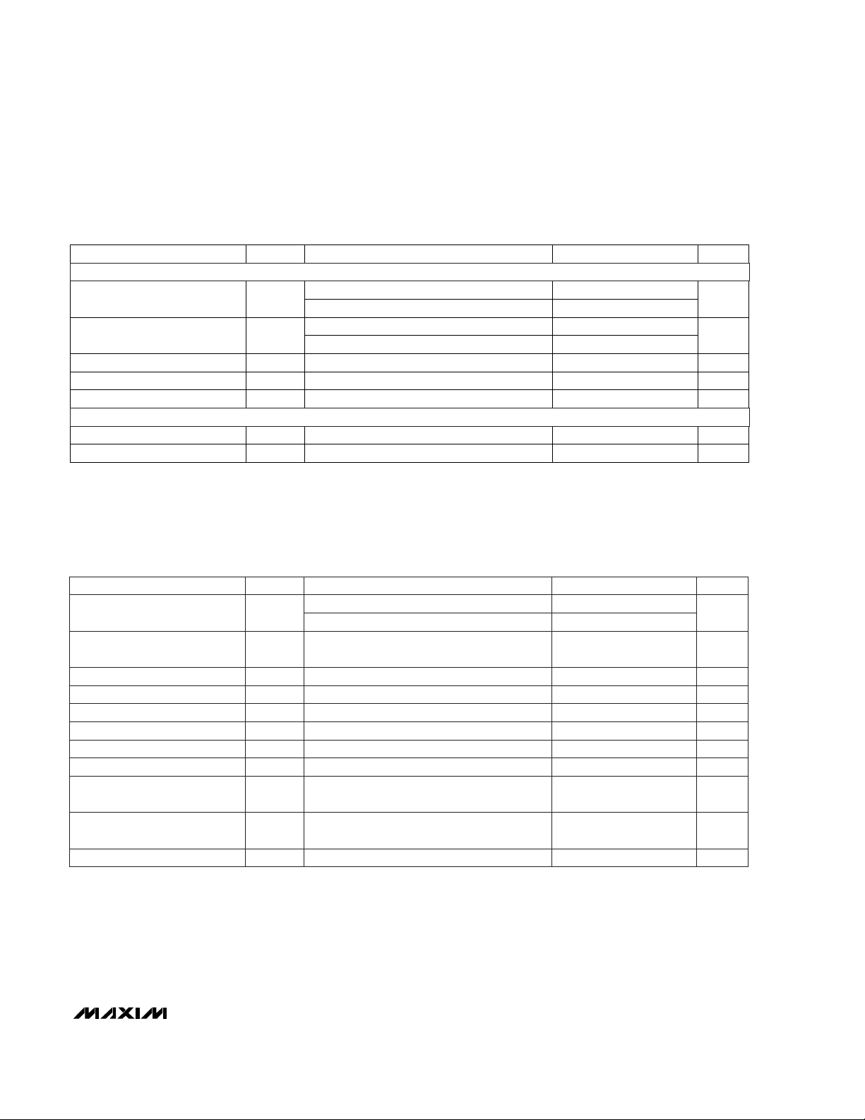
ABSOLUTE MAXIMUM RATINGS
ELECTRICAL CHARACTERISTICS—Single +5V Supply
(V+ = +5V ±5%, TA= T
MIN
to T
MAX
, unless otherwise noted. Typical values are at TA= +25°C.) (Note 2)
Stresses beyond those listed under “Absolute Maximum Ratings” may cause permanent damage to the device. These are stress ratings only, and functional
operation of the device at these or any other conditions beyond those indicated in the operational sections of the specifications is not implied. Exposure to
absolute maximum rating conditions for extended periods may affect device reliability.
V+ to GND................................................................-0.3V to +6V
NO_ _, COM_, DOUT to GND (Note 1) ........-0.3V to (V+ + 0.3V)
SCL, SDA,
CS, SCLK, DIN, A0, A1 to GND..............-0.3V to +6V
Continuous Current into Any Terminal..............................±20mA
Peak Current (NO_ _, COM_ pulsed at 1ms,
10% duty cycle max).....................................................±50mA
Continuous Power Dissipation (T
A
= +70°C)
16-Pin QSOP (derate 8.3mW/°C above +70°C)............667mW
Operating Temperature Ranges
MAX456_CEE....................................................0°C to +70°C
MAX456_EEE.................................................-40°C to +85°C
Storage Temperature Range.............................-65°C to +150°C
Lead Temperature (soldering, 10sec).............................+300°C
VNO_ _ = 4.5V, 1V;
V
COM
_ = 1V, 4.5V;
V+ = 5.25V
I
COM
_ = 4mA;
VNO_ _ = 1V, 2V, 3V;
V+ = 4.75V
I
COM
_ = 4mA,
V
NO
_ _ = 3V,
V+ = 4.75V
CONDITIONS
V0V+
VNO_ _,
V
COM
_
ANALOG SWITCHES
Analog Signal Range (Note 3)
nA
-1 0.001 1
INO_ _
(OFF)
NO_ _ Off-Leakage
Current (Note 6)
Ω
2 5
R
FLAT
On-Resistance
Flatness (Note 5)
Ω
20 30
R
ON
On-Resistance
40
Ω
35
∆R
ON
On-Resistance Match
Between Channels (Note 4)
UNITSMIN TYP MAXSYMBOLPARAMETER
COM_ Off-Leakage
Current (Note 6)
I
COM_(OFF)
V
COM
_ = 1V, 4.5V;
V
NO
_ _ = 4.5V, 1V;
V+ = 5.25V
-1 0.001 1
nA
COM_ On-Leakage
Current (Note 6)
I
COM_(ON)
V
COM
_ = 4.5V, 1V;
VNO_ _ = 4.5V, 1V, or
floating; V+ = 5.25V
-1 0.002 1
nA
Total Harmonic Distortion
plus Noise
THD+N
fIN= 1kHz, VNO_ _ =
1V
RMS
, V
NO_ _
= 2.5V
0.07
%
Channel-to-Channel Crosstalk V
CT(A)
VNO_ _ = 1V
RMS
, fIN= 20kHz, RS= 600Ω,
Figure 1
-85 dB
I
COM
_ = 4mA,
V
NO
_ _ = 3V,
V+ = 4.75V
TA= +25°C
TA= T
MIN
to T
MAX
TA= +25°C
TA= +25°C
TA= +25°C
TA= +25°C
TA= +25°C
7
TA= T
MIN
to T
MAX
TA= T
MIN
to T
MAX
7
TA= T
MIN
to T
MAX
TA= T
MIN
to T
MAX
TA= T
MIN
to T
MAX
-10 10
-10 10
-10 10
Note 1: Signals on NO_ _ or COM_ exceeding V+ or ground are clamped by internal diodes. Limit forward-diode current to maxi-
mum current rating.
Off-Isolation (Note 7) V
ISO(A)
VNO_ _ = 1V
RMS
, fIN= 20kHz, RL= 600Ω,
Figure 1
-85 dB
RL= 600Ω
ANALOG SWITCHES
RL=10kΩ 0.006
AUDIO PERFORMANCE
MAX4562/MAX4563
Serially Controlled, Clickless
Audio/Video Switches
_______________________________________________________________________________________ 3
ELECTRICAL CHARACTERISTICS—Single +5V Supply (continued)
(V+ = +5V ±5%, TA= T
MIN
to T
MAX
, unless otherwise noted. Typical values are at TA= +25°C.) (Note 2)
ELECTRICAL CHARACTERISTICS—Single +3V Supply
(V+ = +3V ±10%, TA= T
MIN
to T
MAX
, unless otherwise noted. Typical values are at TA= +25°C.) (Note 2)
I
COM
_ = 4mA,
V
NO
_ _ = 1V,
V+ = 2.7V
TA= +25°C
TA= T
MIN
to T
MAX
TA= +25°C
7TA= T
MIN
to T
MAX
I
COM
_ = 4mA,
V
NO
_ _ = 1V,
V+ = 2.7V
CONDITIONS
V0V+
VNO_ _,
V
COM
_
ANALOG SWITCHES
Analog Signal Range (Note 3)
Ω
30 60
R
ON
On-Resistance
80
Ω
35
∆R
ON
On-Resistance Match
Between Channels (Note 4)
UNITSMIN TYP MAXSYMBOLPARAMETER
ANALOG SWITCHES
VNO_ _ = 2.5V,
RL= 5kΩ,
CL= 35pF
TA= +25°C
TA= T
MIN
to T
MAX
TA= +25°C
200
fIN= 1MHz
All logic inputs = 0 or V+, TA= T
MIN
to T
MAX
VNO_ _ = 2.5V, TA= T
MIN
to T
MAX
TA= T
MIN
to T
MAX
VNO_ _ = 2.5V,
RL= 300Ω,
CL= 35pF
CONDITIONS
pF10C
OFF(NO)
Off-Capacitance
µA610I+Supply Current (Note 9)
ns10 50t
BBM
Break-Before-Make Time
ns
200 400
t
ONSD
Turn-On Time
500
ns
100 160
t
OFFSD
Turn-Off Time
UNITSMIN TYP MAXSYMBOLPARAMETER
TA= T
MIN
to T
MAX
V2.7 5.5V+Supply Voltage Range
VNO_ _ = 2.5V, RL= 300Ω, CL= 35pF ms3t
OFFSE
Turn-Off Time
VNO_ _ = 2.5V, RL= 5kΩ, CL= 35pF ms12t
ONSE
Turn-On Time
R
SOURCE
= 50Ω, RL= 50Ω MHz300BW-3dB Bandwidth
VNO_ _ = 1V
RMS
, fIN= 10MHz, RS= 50Ω,
Figure 1
dB-55V
CT(V)
Channel-to-Channel Crosstalk
VNO_ _ = 1V
RMS
, fIN= 10MHz, RL= 50Ω,
Figure 1
dB-55V
ISO(V)
Off-Isolation (Note 7)
DYNAMIC TIMING WITH CLICKLESS MODE DISABLED (Note 8, Figure 2)
DYNAMIC TIMING WITH CLICKLESS MODE ENABLED (Note 8, Figure 2)
POWER SUPPLY
VIDEO PERFORMANCE
MAX4562/MAX4563
Serially Controlled, Clickless
Audio/Video Switches
4 _______________________________________________________________________________________
ELECTRICAL CHARACTERISTICS—Single +3V Supply (continued)
(V+ = +3V ±10%, TA= T
MIN
to T
MAX
, unless otherwise noted. Typical values are at TA= +25°C.) (Note 2)
ns
TA= +25°C
TA= +25°C
TA= T
MIN
to T
MAX
-10 10
TA= T
MIN
to T
MAX
CONDITIONS
COM _ On-Leakage
Current (Notes 6, 10)
I
COM_(ON)
V
COM_
= 3V, 0.5V;
VNO_ _ = 3V, 0.5V,
or floating;
V+ = 3.6V
-1 0.002 1
nA
Total Harmonic Distortion
plus Noise
THD+N
fIN= 1kHz, VNO_ _ =
0.5V
RMS
, V
NO_ _
= 1.5V
0.1
%
Off-Isolation (Note 7) V
ISO(A)
V
NO_ _
= 0.5V
RMS
, fIN= 20kHz, RL= 600Ω,
Figure 1
80 dB
Channel-to-Channel Crosstalk V
CT(A)
V
NO_ _
= 0.5V
RMS
, fIN= 20kHz, RS= 600Ω,
Figure 1
85 dB
UNITSMIN TYP MAXSYMBOLPARAMETER
Off-Isolation (Note 7) V
ISO(V)
V
NO_ _
= 0.5V
RMS
, fIN= 10MHz, RL= 50Ω,
Figure 1
-50 dB
Channel-to-Channel Crosstalk V
CT(V)
V
NO_ _
= 0.5V
RMS
, fIN= 10MHz, RS= 50Ω,
Figure 1
-55 dB
-3dB Bandwidth BW R
SOURCE
= 50Ω, RL= 50Ω 200 MHz
Off-Capacitance C
OFF(NO)fIN
= 1MHz 10 pF
Turn-On Time t
ONSD
V
NO_ _
= 1.5V,
RL= 5kΩ, CL= 35pF
400 800
ns
1000
TA= +25°C
TA= T
MIN
to T
MAX
8
On-Resistance
Flatness (Note 5)
R
FLAT
I
COM_
= 4mA;
V
NO_ _
= 1V, 1.5V, 2V;
V
+ = 2.7V
36
Ω
TA= +25°C
TA= T
MIN
to T
MAX
Turn-Off Time t
OFFSD
V
NO_ _
= 1.5V,
RL= 300Ω, CL= 35pF
200 350
500
V
NO_ _
= 1.5V, TA= T
MIN
to T
MAX
Break-Before-Make Time t
BBM
10 100 ns
V
NO_ _
= 1.5V, RL= 5kΩ, CL= 35pFTurn-On Time t
ONSE
12 ms
V
NO_ _
= 1.5V, RL= 300Ω, CL= 35pFTurn-Off Time t
OFFSE
3 ms
TA= +25°C
TA= T
MIN
to T
MAX
-10 10
COM_ Off-Leakage
Current (Notes 6, 10)
I
COM_(OFF)
V
COM
_ = 0.5V, 3V;
V
NO_ _
= 3V, 0.5V;
V+ = 3.6V
-1 0.001 1
nA
TA= +25°C
TA= T
MIN
to T
MAX
-10 10
NO_ _ Off-Leakage
Current (Notes 6, 10)
I
NO_ _(OFF)
V
COM
_ = 0.5V, 3V;
V
NO_ _
= 3V, 0.5V;
V+ = 3.6V
-1 0.001 1
nA
RL = 600Ω
AUDIO PERFORMANCE
VIDEO PERFORMANCE
DYNAMIC TIMING WITH CLICKLESS MODE DISABLED (Notes 8, 12, and Figure 2)
DYNAMIC TIMING WITH CLICKLESS MODE ENABLED (Notes 8, 12, and Figure 2)
RL = 10kΩ 0.01
MAX4562/MAX4563
Serially Controlled, Clickless
Audio/Video Switches
_______________________________________________________________________________________ 5
pF5f = 1MHzC
IN
Input Capacitance
V0.2V
HYST
Input Hysteresis
UNITSMIN TYP MAXCONDITIONSSYMBOLPARAMETER
µA-1 0.001 1Digital inputs = 0 or V+I
LEAK
Input Leakage Current
V+ = 3V
V+ = 3V 0.6
2
V
3V+ = 5V
V
IH
Input High Voltage
V
0.8V+ = 5V
V
IL
Input Low Voltage
VV+ - 0.5 I
SOURCE
= 0.5mAV
OH
DOUT Output High Voltage
I/O INTERFACE CHARACTERISTICS
(V+ = +2.7V to +5.25V, TA= T
MIN
to T
MAX
, unless otherwise noted. Typical values are at TA= +25°C.)
2-WIRE TIMING CHARACTERISTICS
(Figure 3, V+ = +2.7V to +5.25V, f
SCL
= 100kHz, TA= T
MIN
to T
MAX
, unless otherwise noted. Typical values are at TA= +25°C.)
V0.4I
SINK
= 6mAV
OL
Output Low Voltage
DIGITAL INPUTS (SCLK, DIN, CS, SCL, SDA, A0, A1)
DIGITAL OUTPUTS (DOUT, SDA)
UNITSMIN TYP MAXCONDITIONSSYMBOLPARAMETER
ns050Pulse Width of Suppressed Spike
ns
20 +
300
0.1C
b
t
R
SCL/SDA Rise Time
µs4.0t
HIGH
Clock High Period
µs4.7t
LOW
Clock Low Period
ns250t
SU:DAT
Data Setup Time
µs0t
HD:DAT
Data Hold Time
µs4.0t
SU:STO
Stop Condition Setup Time
µs4.7t
BUF
Bus Free Time between Stop
and Start Conditions
0 100V+ = 2.7V to 5.25V
f
SCL
SCL Clock Frequency
ns
20 +
300
0.1C
b
t
F
SCL/SDA Fall Time
µs4.0The first clock is generated after this period t
HD:STA
Hold Time After Start Condition
kHz
400V+ = 4.75V to 5.25V

MAX4562/MAX4563
Serially Controlled, Clickless
Audio/Video Switches
6 _______________________________________________________________________________________
Note 2: The algebraic convention is used in this data sheet; the most negative value is shown in the minimum column.
Note 3: Guaranteed by design. Not subject to production testing.
Note 4: ∆R
ON
= R
ON(MAX)
- R
ON(MIN)
.
Note 5: Resistance flatness is defined as the difference between the maximum and minimum on-resistance values, as measured
over the specified analog signal range.
Note 6: Leakage parameters are 100% tested at maximum rated temperature and guaranteed by correlation at T
A
= +25°C.
Note 7: Off-isolation = 20 log (V
COM
_ / VNO_ _ ), V
COM
_ = output, VNO_ _ = input to off switch.
Note 8: All timing is measured from the clock’s falling edge preceding the ACK signal for 2-wire and from the rising edge of CS for
3-wire. Turn-off time is defined at the output of the switch for a 0.5V change, tested with a 300Ω load to ground. Turn-on
time is defined at the output of the switch for a 0.5V change and measured with a 5kΩ load resistor to GND. All timing is
shown with respect to 20% V+ and 70% V+, unless otherwise noted.
Note 9: Supply current can be as high as 2mA per switch during switch transitions in the clickless mode, corresponding to a 12mA
total supply transient current requirement.
Note 10: Leakage testing is guaranteed by testing with a +5.25V supply.
Note 11: C
b
= capacitance of one bus line in pF. Tested with Cb= 400pF.
Note 12: Typical values are for MAX4563 devices.
15
19
17
21
27
29
25
23
31
012345
ON-RESISTANCE vs. COM_ VOLTAGE
MAX4562 otc01
V
COM
_ (V)
ON-RESISTANCE (Ω)
V+ = 2.7V
V+ = 3.3V
V+ = 5.0V
12
14
13
16
15
17
18
20
19
21
012345
ON-RESISTANCE vs. COM_ VOLTAGE
AND TEMPERATURE
MAX4562 TOC02
V
COM_
(V)
ON-RESISTANCE (Ω)
TA = +70°C
TA = +85°C
TA = +25°C
TA = -40°C
0.1
1
100
10
1000
-40 -15 10 35 60 85
LEAKAGE CURRENT vs. TEMPERATURE
MAX4562/3toc03
TEMPERATURE (°C)
CURRENT (pA)
COM_ON
NO_ _OFF
COM_OFF
Typical Operating Characteristics
(V+ = +5V, TA = +25°C, unless otherwise noted.)
3-WIRE TIMING CHARACTERISTICS
(Figure 5, V+ = +2.7V to +5.25V, fOP= 2.1MHz, TA= T
MIN
to T
MAX
, unless otherwise noted. Typical values are at TA= +25°C.)
SCLK Pulse Width High t
CH
200
V+ = 4.75V to 5.25V 10
ns
Fall Time (SCLK, DIN, CS)
t
F
2 µs
SCLK Pulse Width Low t
CL
200 ns
CS Fall to SCLK Rise Hold
t
CSH
0 ns
Rise Time (SCLK, DIN, CS)
t
R
DIN to SCLK Setup t
DS
100 ns
Operating Frequency f
OP
V+ = 2.7V to 5.25V 0 2.1
MHz
DIN to SCLK Hold t
DH
0 ns
2 µs
CS Fall to SCLK Rise Setup
t
CSS
100 ns
PARAMETER SYMBOL CONDITIONS MIN TYP MAX UNITS
CS Pulse Width High
t
CSW
40 ns
SCLK Fall to Output Data Valid t
DO
C
LOAD
= 50pF 200 ns

MAX4562/MAX4563
Serially Controlled, Clickless
Audio/Video Switches
_______________________________________________________________________________________
7
10 1000100 10,000 100,000
TOTAL HARMONIC DISTORTION PLUS
NOISE vs. FREQUENCY
MAX4562 toc07
FREQUENCY (Hz)
THD+N (%)
1
0.01
0.1
600Ω IN AND OUT
SIGNAL = 1V
RMS
10 1k100 10k 100k
AUDIO FREQUENCY RESPONSE
MAX4526 toc08
FREQUENCY (Hz)
LOSS (dB)
0
-20
-120
-100
-60
-80
-40
600Ω IN AND OUT
OFF-ISOLATION
CROSSTALK
0
-20
-100
0.1 10 100
VIDEO FREQUENCY RESPONSE
-40
-60
-80
MAX4562 toc09
FREQUENCY (MHz)
LOSS (dB)
1
INSERTION LOSS
OFF-ISOLATION
CROSSTALK
50Ω IN AND OUT
5ms/div
TURN-ON AND TURN-OFF TIMES
(SOFT MODE)
MAX4562 toc10
CS
(5V/div)
t
OFF
(1V/div)
t
ON
(1V/div)
Typical Operating Characteristics (continued)
(V+ = +5V, TA= +25°C, unless otherwise noted.)
100ns/div
TURN-ON AND TURN-OFF TIMES
(HARD MODE)
MAX4562 toc13
CS
(5V/div)
t
ON
(1V/div)
t
OFF
(1V/div)
5.1
5.3
5.2
5.5
5.4
5.6
5.7
-40 10-15 35 60 85
SUPPLY CURRENT vs. TEMPERATURE
MAX4562/3toc04
TEMPERATURE (°C)
SUPPLY CURRENT (µA)
-3
-1
-2
1
0
2
3
021 345
CHARGE INJECTION vs. COM_ VOLTAGE
MAX4562 toc05
V
COM_
(V)
Q (pC)
0
100
50
200
150
250
300
-40 10-15 35 60 85
TURN-ON AND TURN-OFF TIMES
vs. TEMPERATURE (HARD MODE)
MAX4562/3toc06
TEMPERATURE (°C)
TIME (ns)
tON, V+ = +3V
tON, V+ = +5V
t
OFF
, V+ = +3V
t
OFF
, V+ = +5V

MAX4562/MAX4563
Serially Controlled, Clickless
Audio/Video Switches
8 _______________________________________________________________________________________
Pin Description
NO1A, NO1B,
NO2A, NO2B,
NO3, NO4
2, 4, 6, 8,
10, 12
Normally Open Terminals
COM1–COM43, 7, 9, 11 Common Terminals
A113
A0
SDA
SCL
GND5
LSB + 2 of 2-Wire Serial Interface Address Field
LSB + 1 of 2-Wire Serial Interface Address Field
Data Input of 2-Wire Serial Interface
Clock Input of 2-Wire Serial Interface
Ground
V+1 Positive Supply Voltage
NAME FUNCTION
Typical Operating Characteristics (continued)
(V+ = +5V, TA= +25°C, unless otherwise noted.)
DOUT Data Input of 3-Wire Serial Interface
CS
14
Chip-Select of 3-Wire Serial Interface
DIN
15
Data Input of 3-Wire Serial Interface
SCLK Clock Input of 3-Wire Serial Interface
1
2, 4, 6, 8,
10, 12
3, 7, 9, 11
5
–
–
–
–
PIN
13–
14–
MAX4562 MAX4563
15–
–
16
16
SOFT-MODE RISE TIME
AMPLITUDE (500mV/div)
500µs/div
MAX4562 toc11
AMPLITUDE (500mV/div)
SOFT-MODE FALL TIME
MAX4562 toc12
500µs/div

MAX4562/MAX4563
Serially Controlled, Clickless
Audio/Video Switches
_______________________________________________________________________________________ 9
Figure 2. Switching Time
DECODER/
CONTROLLER
DECODER/
CONTROLLER
2/3
SIGNAL
GENERATOR 0dBm
V+
10nF
ANALYZER
NO_ _
R
L
GND
COM_
V+
2/3
SIGNAL
GENERATOR 0dBm
V+
10nF
ANALYZER
a) OFF-ISOLATION
b) CROSSTALK
NO2A
R
L
GND
COM1
NO1
B
50Ω
COM2
N.C.
V+
MAX4562
MAX4563
Figure 1. Off-Isolation and Crosstalk
ACKNOWLEDGE
BIT
tR < 20ns
t
< 20ns
F
MAX4562
SCL
3V
50%
0
MAX4563
V
CS
V
V
V
OUT
0
OUT
0
3V
0
OUT
0
OUT
0
50%
-0.5V
t
ON
V
0.5V
OUT -
t
OFF
•
0.9
V
OUT
t
ON
0.1 • V
t
OFF
OUT
V+
10nF
V+
µP
V
NO_ _
NO_ _
2 OR 3
SERIAL
INTERFACE
DECODER/
CONTROLLER
GND
COM _
R
L
300Ω
C
L
35pF
V
OUT
INCLUDES FIXTURE AND STRAY CAPACITANCE.
C
L
= V
OUT
[RL / (RL + RON)]
COM
V
2-WIRE
3-WIRE

MAX4562/MAX4563
Serially Controlled, Clickless
Audio/Video Switches
10 ______________________________________________________________________________________
Detailed Description
The MAX4562/MAX4563 are serial-interface controlled
switches with soft-mode “clickless” and hard-mode operating capability. The MAX4562/MAX4563 contain two
SPST switches and two SPDT switches. The SPDT
switches are actually 2-to-1 multiplexers, in that each
SPDT is really two independent SPST switches with a
common node, as shown in the
Pin Configuration
. Each
switch is controlled independently by either the 2-wire
I2C-compatible or 3-wire SPI/QSPI/MICROWIRE-compatible serial interface.
Audio off-isolation and crosstalk is -85dB at 20kHz.
Video off-isolation and crosstalk is at least -55dB at
10MHz.
Each switch of either device may be set to operate in
either soft or hard mode. In soft mode, the switching
transition is slowed to avoid the audible “clicking” that
can occur when switches are used to route audio signals. In hard mode, the switches are not slowed down,
making this mode useful when a faster response is
required. If a new command is issued while any softmode switch is transitioning, the switch transition time is
decreased so it reaches its final state before the new
command is executed. Soft mode and open are the
power-up default states for all switches. Switches in the
same mode are guaranteed to be break-before-make
relative to each other. Break-before-make does not apply
between switches operating in different modes.
These devices operate from a +2.7V to +5.5V single
supply. The MAX4562 features a 2-wire I2C-compatible
serial interface, and the MAX4563 features a 3-wire
SPI/QSPI/MICROWIRE-compatible serial interface.
SCL
SDA
t
LOW
t
HIGH
t
F
t
R
tHD,
STA
tHD,
DAT
tHD,
STA
tSU,
DAT
tSU,
STA
t
BUF
tSU,
STO
START CONDITIONSTOP CONDITIONREPEATED START CONDITIONSTART CONDITION
20%
70%
20%
70%
20%
70%
20%
70%
20%
70%
20%
70%
20%
70% 70%
20%
70% 70% 70%
Figure 3. 2-Wire Serial-Interface Timing Diagram
START CONDITION STOP CONDITION
COMMAND BYTE
SLAVE ADDRESS BYTE
SCL
SDA
MSB
MSB
LSB LSBACK ACK
Figure 4. A Complete 2-Wire Serial-Interface Transmission

MAX4562/MAX4563
Serially Controlled, Clickless
Audio/Video Switches
______________________________________________________________________________________ 11
Table 1. Command-Bit Mapping
C1 C0 COMMAND DESCRIPTION
0 0 NO_OP No Operation
0 1 NO_OP No Operation
1 0 SWITCHSET Sets specified switches open or closed.
1 1 MODESET Sets specified switches to soft or hard mode.
Applications Information
Switch Control
The MAX4562/MAX4563 have a common commandand control-bit structure; the only difference is the interface type (2-wire or 3-wire).
The SWITCHSET command controls the open/closed
states of the various switches. MODESET controls
soft/hard-mode switch states. The NO_OP command is
useful for daisy-chaining multiple 3-wire parts.
Table 1 shows the command bits’ configuration and their
related commands. Table 2 shows the configuration of
the data bits and their related switches. After a SWITCHSET command is issued, a logic “1” in any data-bit location closes the associated switch, while a logic “0”
opens it. After a MODESET command, a logic “1” in any
data-bit location sets the associated switch into soft
mode, while a logic “0” sets it into hard mode.
2-Wire Serial Interface
The MAX4562 uses a 2-wire I2C-compatible serial interface, requiring only two I/O lines of a standard microprocessor port for communication. These devices use
a SendByte™ protocol. The SendByte protocol consists
of one byte of address field followed by one byte of
command field.
The first byte of any 2-wire serial-interface transaction is
always the address byte. To address a given chip, the
A0 and A1 bits in the address byte (Table 3) must duplicate the values present at the A0 and A1 pins of that
chip, and the rest of the address bits must be configured
as shown in Table 3. Connect the A0 and A1 pins to V+
or GND or drive them with CMOS logic levels.
The second byte is the command byte, which sets the
command being written to the device. The possible
commands are MODESET and SWITCHSET. Figures 3
and 4 and the
I/O Interface Characteristics
detail the timing of the 2-wire serial-interface protocol. All bytes of the
transmission, whether address or command, are sent
MSB first.
The MAX4562/MAX4563 are receive-only devices and
must be controlled by a bus master device. A bus master signals the beginning of a transmission with a start
condition by transitioning SDA from high to low while
SCL is high. The slave devices monitor the serial bus
continuously, waiting for the start condition followed by
an address byte. When a device recognizes its address
byte, it acknowledges by pulling the SDA line low for one
clock period; it is then ready to accept the command
byte. The device also issues a similar acknowledgment
after the command byte. When the master has finished
communicating with the slave, it issues a stop condition
by transitioning SDA from low to high while SCL is high.
The bus is then free for another transmission.
3-Wire Serial Interface
The MAX4563 uses a 3-wire SPI/QSPI/MICROWIRE-compatible serial interface. An active-low chip select (CS) pin
enables the device to receive data from the serial input
pin, DIN. Command and data information are clocked in
on the rising edge of the serial clock signal (SCLK) MSB
first. A total of eight bits is needed in each write cycle.
The command code is contained in the two MSBs of the
8-bit word. The remaining bits control the switches as
shown in Table 4. While shifting in the serial data, the
device remains in its original configuration. A rising edge
on CS latches the data into the MAX4563’s internal regis-
ter, initiating the device’s change of state. Table 4 shows
the details of the 3-wire interface structure.
Table 2. Control-Bit Mapping
CONTROL BIT SWITCH SWITCH TERMINAL
D1
D5 SW1A 2, 3
SW3
D4 SW1B 3, 4
9, 10
D3 SW2A 6, 7
D0 (LSB)
D2 SW2B 7, 8
SW4 11, 12
SendByte is a trademark of Philips Corp.

Figures 5 and 6 and the
I/O Interface Characteristics
show the timing details of the 3-wire interface. If the two
command bits initiate a SWITCHSET command, a logic
“1” in a switch control location closes the associated
switch, while a logic “0” opens it. If the command bits initiate a MODESET command, a logic “1” in a switch control location sets the associated switch into soft
“clickless” mode, while a logic “0” sets it into hard mode.
For command-bit configurations, see Table 1.
Using Multiple Devices
There are two ways to connect multiple devices to the
same 3-wire serial interface. The first involves using the
DOUT pin. DOUT presents a copy of the last bit of the
internal shift register, useful for daisy-chaining multiple
devices. Data at DOUT are simply the input data
delayed by eight clock cycles, appearing synchronous
with SCLK’s falling edge. After CS goes high, DOUT
holds the last bit in the shift register until new data are
shifted into DIN. For a simple interface using several
MAX4563 devices, daisy-chain the shift registers by
connecting DOUT of the first device to DIN of the second, etc. Connect the CS pins of all devices together.
Data are shifted through the MAX4563 in series. When
CS is brought high, all devices are updated simultaneously. If any of the devices in the chain are to be left
unchanged, use a NO_OP command for that device, as
shown in Table 1.
An alternate way of connecting multiple devices is to
decode the CS line. In this case, do not use the DOUT
pin and connect the DIN pins of all devices together.
Address decode logic individually controls the CS line
of each device. When a device is to be selected, its CS
line is brought low, data are shifted in, and its CS line is
then brought high to execute the command.
For command bit configuration see Table 1.
T-Switches
Configure the MAX4562/MAX4563 as a T-switch to
improve off-isolation. As the signal frequency is increased, parasitic capacitance significantly degrades
the off-isolation. Figure 7 shows a typical T-switch configuration using the MAX4562/MAX4563 to improve offisolation. COM2 and COM3 are tied together to create
a single common node. NO2A and NO2B act as the
input and output of the T-switch, while NO3 is tied to
ground. When both SW2A and SW2B are closed, SW3
should be open to allow the signal to pass into NO2A
and out of NO2B. However, when SW2A and SW2B are
open, energy that is coupled through the open switches is shunted to ground through SW3, which should
now be closed. This increases the off-isolation to typically -68dB at 10MHz (Figure 8).
MAX4562/MAX4563
Serially Controlled, Clickless
Audio/Video Switches
12 ______________________________________________________________________________________
Table 3. MAX4562 2-Wire Serial-Interface Data Format
Table 4. MAX4563 3-Wire Serial-Interface
Data Format
SWITCH CONTROLCOMMAND
D1D3 D0
MSB LSB
D2D5 D4D6D7
SW3SW2A SW4SW3BSW1A SW1BC0C1
1SRT
STP = Stop Condition
Logic “0” in any data bit location places the associated switch open or in hard switching mode.
Logic “1” in any data bit location places the associated switch closed or in soft (clickless) switching mode.
See Table 1 for command-bit configuration.
1 0 0 1 C1A1 A0 0 ACK C0 SW2A SW1B SW2B SW3 SW4 ACK STPSW2A
ADDRESS BYTE COMMAND BYTE
MSB LSB MSB LSB

MAX4562/MAX4563
Serially Controlled, Clickless
Audio/Video Switches
______________________________________________________________________________________ 13
SCLK
DIN
DOUT
t
CSS
t
CL
t
CH
t
CSW
t
CSO
t
DO
t
CSH
t
DH
t
DS
D7
D6
D1 D0
CS
20%
20% 20% 20% 20% 20%
20%
70%
70%
70%
70%
Figure 5. 3-Wire Serial-Interface Timing Diagram
D7 D6 D5 D4
MSB
LSB
D3 D2 D1 D0
DATA BITS FROM PREVIOUS DATA INPUT
DOUT POWER-UP DEFAULT: D7–D0 = 0
D6 D5 D4 D3 D2 D1 D0
D7
DOUT
DIN
SCLK
SWITCHES UPDATED
DATA CLOCKED IN
DATA CLOCKED OUT
CS
D7
INPUT DATA BITS
Figure 6. A Complete 3-Wire Serial-Interface Transmission
-20
-40
-120
0.1 10 100
-100
-60
-80
FREQUENCY (MHz)
OFF-ISOLATION (dB)
1
T-SWITCH
SPST
SWITCH
Figure 8. Off-Isolation vs. Frequency
SIGNAL OUTSIGNAL IN
COM3
NO3
NO2B
NO2A
COM2
Figure 7. T-Switch Configuration
TRANSISTOR COUNT: 3518
___________________Chip Information

MAX4562/MAX4563
Serially Controlled, Clickless
Audio/Video Switches
14 ______________________________________________________________________________________
Package Information
QSOP.EPS

MAX4562/MAX4563
Serially Controlled, Clickless
Audio/Video Switches
______________________________________________________________________________________ 15
NOTES

MAX4562/MAX4563
Serially Controlled, Clickless
Audio/Video Switches
Maxim cannot assume responsibility for use of any circuitry other than circuitry entirely embodied in a Maxim product. No circuit patent licenses are
implied. Maxim reserves the right to change the circuitry and specifications without notice at any time.
16
____________________Maxim Integrated Products, 120 San Gabriel Drive, Sunnyvale, CA 94086 408-737-7600
© 1999 Maxim Integrated Products Printed USA is a registered trademark of Maxim Integrated Products.
NOTES
 Loading...