

Page 1
For free samples & the latest literature: http://www.maxim-ic.com, or phone 1-800-998-8800.
For small orders, phone 1-800-835-8769.
General Description
The MAX4558/MAX4559/MAX4560 are low-voltage,
CMOS analog ICs configured as an 8-to-1 multiplexer
(MAX4558), a dual 4-to-1 multiplexer (MAX4559), and a
triple single-pole/double-throw (SPDT) switch
(MAX4560). Each switch is protected against ±15kV
electrostatic discharge (ESD) shocks, without latchup
or damage.
These CMOS devices can operate continuously from
dual supplies of ±2V to ±6V or from a +2V to +12V single supply. Each switch can handle Rail-to-Rail®analog signals. The off-leakage current is only 1nA at
+25°C or 10nA at +85°C max.
All digital inputs have +0.8V to +2.4V logic thresholds,
ensuring TTL/CMOS-logic compatibility when using a
single +5V supply or dual ±5V supplies.
Applications
Battery-Operated Equipment
Audio and Video Signal Routing
Low-Voltage Data-Acquisition Systems
Communications Circuits
High-ESD Environments
Features
♦ ESD-Protected X, Y, Z and X_, Y_, Z_ Pins
±15kV (Human Body Model)
±12kV (IEC 1000-4-2, Air-Gap Discharge)
±8kV (IEC 1000-4-2, Contact Discharge)
♦ Pin-Compatible with Industry-Standard
74HC4051/74HC4052/74HC4053
♦ Guaranteed On-Resistance
220Ω with Single +5V Supply
160Ω with ±5V Supply
♦ R
ON
Match Between Channels: 2Ω (typ)
♦ Guaranteed Low leakage Currents
1nA Off-Leakage (at +25°C)
1nA On-Leakage (at +25°C)
♦ TTL-Compatible Inputs with +5V/±5V Supplies
♦ Low Distortion: < 0.02% (600Ω)
♦ Low Crosstalk: < -93dB (50Ω)
♦ High Off-Isolation: < -96dB (50Ω)
MAX4558/MAX4559/MAX4560
±15kV ESD-Protected, Low-Voltage, CMOS
Analog Multiplexers/Switches
________________________________________________________________
Maxim Integrated Products
1
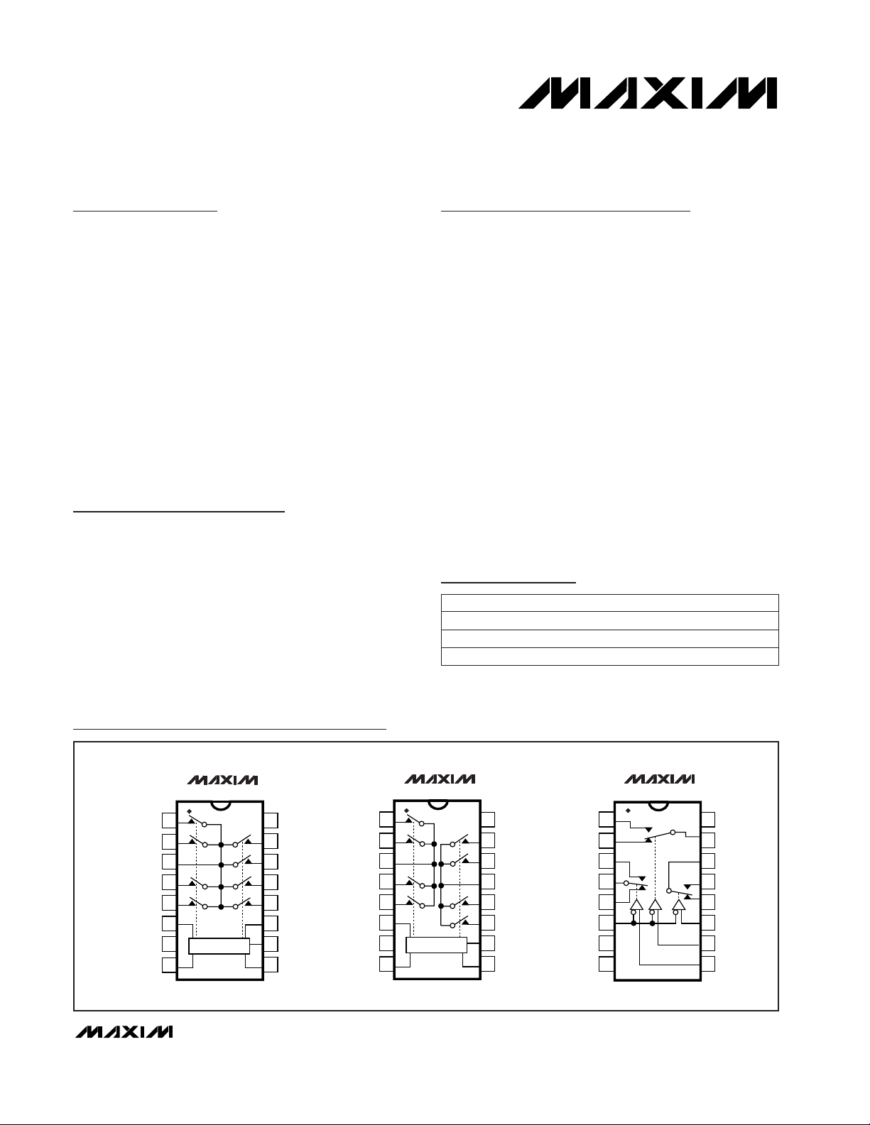
16
15
14
13
12
11
10
9
1
2
3
4
5
6
7
8
V
CC
X2
X1
X0
X3
A
B
C
X4
X6
X
X7
X5
ENABLE
V
EE
GND
TOP VIEW
MAX4558
DIP/SO/QSOP
LOGIC
16
15
14
13
12
11
10
9
1
2
3
4
5
6
7
8
V
CC
Y
X
X1
X0
A
B
C
Y1
Y0
Z1
Z
Z0
ENABLE
V
EE
GND
MAX4560
DIP/SO/QSOP
16
15
14
13
12
11
10
9
1
2
3
4
5
6
7
8
V
CC
X2
X1
X
X0
X3
A
B
Y0
Y2
Y
Y3
Y1
ENABLE
V
EE
GND
MAX4559
DIP/SO/QSOP
LOGIC
19-1443; Rev 0; 4/99
PART
MAX4558CEE
MAX4558CSE
MAX4558CPE 0°C to +70°C
0°C to +70°C
0°C to +70°C
TEMP. RANGE PIN-PACKAGE
16 QSOP
16 Narrow SO
16 Plastic DIP
Ordering Information continued at end of data sheet.
Pin Configurations/Functional Diagrams
Ordering Information
Rail-to-Rail is a registered trademark of Nippon Motorola, Ltd.
Page 2
MAX4558/MAX4559/MAX4560
±15kV ESD-Protected, Low-Voltage, CMOS
Analog Multiplexers/Switches
2 _______________________________________________________________________________________
ABSOLUTE MAXIMUM RATINGS
ELECTRICAL CHARACTERISTICS—Dual ±5V Supplies
(VCC= +4.5V to +5.5V, VEE= -4.5V to -5.5V, V_H= +2.4V, V_L= +0.8V, TA= T
MIN
to T
MAX
, unless otherwise noted. Typical values
are at T
A
= +25°C.)
Stresses beyond those listed under “Absolute Maximum Ratings” may cause permanent damage to the device. These are stress ratings only, and functional
operation of the device at these or any other conditions beyond those indicated in the operational sections of the specifications is not implied. Exposure to
absolute maximum rating conditions for extended periods may affect device reliability.
Note 1: Signals on any terminal exceeding VCCor VEEare clamped by internal diodes. Limit forward diode current to maximum cur-
rent rating.
(Voltages referenced to V
EE
)
V
CC
........................................................................ -0.3V to +13V
Voltage into Any Terminal (Note 1).... (V
EE
- 0.3V) to (VCC+ 0.3V)
Continuous Current into Any Terminal .............................±10mA
Peak Current, X, Y, Z, X_, Y_, Z_
(pulsed at 1ms, 10% duty cycle) ..................................±30mA
ESD per Method IEC 1000-4-2 (X, Y, Z, X_, Y_, Z_)
Air-Gap Discharge......................................................... ±12kV
Contact Discharge............................................................±8kV
ESD per Method 3015.7
V
CC
, VEE, A, B, C, ENABLE, GND ................................ ±2.5kV
X, Y, Z, X_, Y_, Z_............................................................±15kV
Continuous Power Dissipation (T
A
= +70°C)
QSOP (derate 8.00mW/°C above +70°C).................... 640mW
Narrow SO (derate 8.70mW/°C above +70°C) .............696mW
DIP (derate 10.53mW/°C above +70°C).......................842mW
Operating Temperature Ranges
MAX45_ _C_E ......................................................0°C to +70°C
MAX45_ _E_E ...................................................-40°C to +85°C
Storage Temperature Range.............................-65°C to +150°C
Lead Temperature (soldering, 10sec).............................+300°C
VV- V+
VX_, VY_,
VZ_, VX,
VY, V
Z
Analog Signal Range
VCC= 4.5V; VEE= -4.5V;
IX, IY, IZ= 1mA; VX_, VY_, VZ_= ±3V
Ω
180
R
ON
On-Resistance
110 160
VCC= 4.5V; V
EE
= -4.5V;
IX, IY, IZ= 1mA; VX_, VY_, VZ_= -3V, 0V, 3V
VCC= 4.5V; V
EE
= -4.5V;
IX, IY, IZ= 1mA; VX_, VY_, VZ_= ±3V
38
On-Resistance Flatness
(Note 4)
Ω
26
∆R
ON
On-Resistance Match
Between Channels (Note 3)
VCC= 5.5V; VEE= -5.5V;
VX_, VY_, VZ_= 4.5V, -4.5V;
VX, VY, VZ= -4.5V, 4.5V
-20 20
-2 0.002 2
VCC= 5.5V; VEE= -5.5V;
VX_, VY_, VZ_= 4.5V, -4.5V;
VX, VY, VZ= -4.5V, 4.5V
nA
-1 0.002 1
I
X_(OFF)
,
I
Y_(OFF)
,
I
Z_(OFF)
X_, Y_ , Z_ Off-Leakage
Current (Note 5)
nA
-10 0.002 10
I
X(OFF)
,
I
Y(OFF)
,
I
Z(OFF)
X, Y, Z Off-Leakage Current
(Note 5)
-1 0.002 1
Ω
10
C, E
C, E
+25°C
+25°C
+25°C
+25°C
C, E
+25°C
C, E
C, E
+25°C
CONDITIONS UNITS
MIN TYP MAX
(Note 2)
SYMBOLPARAMETER T
A
C, E
R
FLAT(ON)
C, E -10 10
MAX4558
MAX4559
MAX4560
MAX4558
MAX4559
MAX4560
-20 20
-2 0.002 2
VCC= 5.5V; VEE= -5.5V;
VX_, VY_, VZ_= 4.5V, 4.5V;
VX, VY, VZ= 4.5V, -4.5V
nA
-10 0.002 10
I
X(ON)
,
I
Y(ON)
,
I
Z(ON)
X, Y, Z On-Leakage Current
(Note 5)
-1 0.002 1
C, E
+25°C
C, E
+25°C
8
ANALOG SWITCH
Page 3
MAX4558/MAX4559/MAX4560
±15kV ESD-Protected, Low-Voltage, CMOS
Analog Multiplexers/Switches
_______________________________________________________________________________________ 3
ELECTRICAL CHARACTERISTICS—Dual ±5V Supplies (continued)
(VCC= +4.5V to +5.5V, VEE= -4.5V to -5.5V, V_H= +2.4V, V_L= +0.8V, TA= T
MIN
to T
MAX
, unless otherwise noted. Typical values
are at T
A
= +25°C.)
V
0.8
VA_, VB_,
VC_, V
EN
Input Logic High 2.4
CONDITIONS UNITS
MIN TYP MAX
(Note 2)
SYMBOLPARAMETER T
A
C, E
C, E
VA_, VB_,
VC_, V
EN
Input Logic Low V
VA, VB, VC, VEN= VCCor 0 µA
VA_, VB_,
VC_, V
EN
Input Current Logic
High or Low
-1 1C, E
VCC, V
EE
±2 ±6
VCC= 5.5V; VEE= -5.5V;
VA, VB, VC, VEN= 0 or V
CC
µAI
CC
Supply Current,
VCCor V
EE
Power-Supply Range
-1 1+25°C
VC, E
90 150
VX, VY, VZ= 0; RS= 0; CL= 1nF;
Figure 3
pC
Q
Charge Injection 2.4+25°C
VX_, VY_, VZ_= 0; f = 1MHz;
Figure 5
pF
C
X_(OFF)
,
C
Y_(OFF)
,
C
Z_(OFF)
VX_, VY_, VZ_Off-Capacitance 2.5
6
10
+25°C
+25°C
VX, VY, VZ= GND; f = 1MHz;
Figure 5
pF
C
X(OFF
),
C
Y(OFF
),
C
Z(OFF)
VX, VY, VZOff-Capacitance
4
+25°C
VX_, VY_, VZ_= 3V; RL= 300Ω; CL= 35pF;
Figure 1
175
t
ON
Turn-On Time ns
C, E
VX_, VY_, VZ_= 3V; RL= 300Ω; CL= 35pF;
Figure 1
150
t
OFF
Turn-Off Time ns
C, E
55 120+25°C
VX_, VY_, VZ_= 3V; RL= 300Ω; CL= 35pF;
Figure 1
175
t
TRANS
Address Transition Time ns
C, E
VX_, VY_, VZ_= 3V; RL= 300Ω; CL= 35pF;
Figure 2
415t
OPEN
Break-Before-Make Delay ns
90 150
+25°C
+25°C
MAX4558
MAX4559
MAX4560
11
15
VX_, VY_, VZ_= GND;
f = 1MHz; Figure 5
pFC
ON
Switch On-Capacitance
9
+25°C
MAX4559
MAX4558
MAX4560
C, E -10 10
DIGITAL I/O
POWER SUPPLY
SWITCH DYNAMIC CHARACTERISTICS
Page 4
C, E ΩTotal Harmonic Distortion THD 180
RL= 600Ω, TBD = 5Vp-p, f = 20Hz to
MAX4558/MAX4559/MAX4560
±15kV ESD-Protected, Low-Voltage, CMOS
Analog Multiplexers/Switches
4 _______________________________________________________________________________________
ELECTRICAL CHARACTERISTICS—Dual ±5V Supplies (continued)
(VCC= +4.5V to +5.5V, VEE= -4.5V to -5.5V, V_H= +2.4V, V_L= +0.8V, TA= T
MIN
to T
MAX
, unless otherwise noted. Typical values
are at T
A
= +25°C.)
mA
110+25°C
CL= 15pF; RL= 50Ω; f = 100kHz;
VX_, VY_, VZ_= 1V
RMS
; Figure 4
-96
CONDITIONS UNITS
MIN TYP MAX
(Note 2)
SYMBOLPARAMETER T
A
V
ISO
Off-Isolation dB+25°C
CL= 15pF; RL= 50Ω; f = 100kHz;
VX_, VY_, VZ_= 1V
RMS
; Figure 4
dBV
CT
Channel-to-Channel Crosstalk -93+25°C
I
H+
ESD SCR Positive Holding
Current
70+85°C
I
H-
ESD SCR Negative Holding
Current
65+85°C
mA
95+25°C
RL= 600Ω; VX_, VY_, VZ_= 5Vp-p;
f = 20Hz to 20kHz
0.02THDTotal Harmonic Distortion %+25°C
ELECTRICAL CHARACTERISTICS—Single +5V Supply
(VCC= +4.5V to +5.5V, VEE= 0, V_H= +2.4V, V_L= +0.8V, TA= T
MIN
to T
MAX
, unless otherwise noted. Typical values are at
T
A
= +25°C.)
C, E
VCC= 4.5V; IX, IY, IZ= 1mA;
VX, VY, VZ= 3V
Ω
350
R
ON
On-Resistance
150 220
C, E -10 10
VCC= 4.5V; IX, IY, IZ= 1mA;
VX, VY, VZ= 3V
MAX4558
Ω
MAX4558
310
∆R
ON
MAX4559
MAX4560
MAX4559
MAX4560
V0V+
VX_, VY_,
VZ_, VX,
VY, V
Z
Analog Signal Range
-20 20
-2 0.002 2
VCC= 5.5V;
VX_, VY_, VZ_= 1V, 4.5V;
VX, VY, VZ= 1V, 4.5V
On-Resistance Match
Between Channels
(Note 3, 6)
nA
-10 0.002 10
I
X(ON)
,
I
Y(ON)
,
I
Z(ON)
X, Y, Z On-Leakage Current
(Note 6)
VCC= 5.5V; VX, VY, VZ= 1V, 4.5V,
VX, VY, VZ= 4.5V, 1V
-1 0.002 1
C, E
+25°C
-20 20
C, E
+25°C
12
-2 0.002 2
VCC= 5.5V;
VX_, VY_, VZ_= 1V, 4.5V;
VX, VY, VZ= 4.5V, 1V
nA
-1 0.002 1
I
X_(OFF)
,
I
Y_(OFF)
,
I
Z_(OFF)
X_, Y_ , Z_ Off-Leakage
Current (Note 6)
nA
-10 10
I
X(OFF)
,
I
Y(OFF)
,
I
Z(OFF)
X, Y, Z Off-Leakage Current
(Note 6)
-1 0.002 1
CONDITIONS UNITS
MIN TYP MAX
(Note 2)
SYMBOLPARAMETER T
A
C, E
C, E
+25°C
+25°C
+25°C
C, E
+25°C
C, E
+25°C
ANALOG SWITCH
Page 5
MAX4558/MAX4559/MAX4560
±15kV ESD-Protected, Low-Voltage, CMOS
Analog Multiplexers/Switches
_______________________________________________________________________________________ 5
ELECTRICAL CHARACTERISTICS—Single +5V Supply (continued)
(VCC= +4.5V to +5.5V, VEE= 0, V_H= +2.4V, V_L= +0.8V, TA= T
MIN
to T
MAX
, unless otherwise noted. Typical values are at
T
A
= +25°C.)
VX_, VY_, VZ_= 3V; RL= 300Ω; CL= 35pF;
Figure 1
V
0.8
VA_, VB_,
VC_, V
EN
Input Logic High
VA_, VB_,
VC_, V
EN
2.4
VA, VB, VC,V
EN
= VCCor 0 µA
300
VA_, VB_,
V
C_
, V
EN
Input Current Logic
High or Low
Input Logic Low
t
ON
-1 1
Turn-On Time ns
C, E
C, E
VX_, VY_, VZ_= 3V; RL= 300Ω; CL= 35pF;
Figure 1
V
200
t
OFF
Turn-Off Time ns
C, E
50 150
110 250
VX, VY, VZ= 2.5V; RS= 0; CL= 1nF;
Figure 3
pCQCharge Injection
+25°C
1+25°C
+25°C
CONDITIONS UNITS
MIN TYP MAX
(Note 2)
SYMBOLPARAMETER T
A
VX_, VY_, VZ_= 3V; RL= 300Ω; CL= 35pF;
Figure 1
300
t
TRANS
Address Transition Time ns
C, E
VX_, VY_, VZ_= 3V; RL= 300Ω; CL= 35pF;
Figure 3
10t
OPEN
Break-Before-Make Delay ns
110 250
C, E
+25°C
C, E
C, E
VCC, V
EE
VPower-Supply Range +2 +12C, E
VCC= 5.5V; VAH, VBH, VCH, V
EN
= 0 or V
CC
µAI
CC
V
CC
Supply Current
-1 1+25°C
C, E -10 10
DIGITAL I/O
POWER SUPPLY
SWITCH DYNAMIC CHARACTERISTICS (Note 6)
Page 6

MAX4558/MAX4559/MAX4560
±15kV ESD-Protected, Low-Voltage, CMOS
Analog Multiplexers/Switches
6 _______________________________________________________________________________________
ELECTRICAL CHARACTERISTICS—Single +3V Supply
(VCC= +2.7V to +3.6V, V_H= +2.0V, V_L= +0.8V, TA= T
MIN
to T
MAX
, unless otherwise noted. Typical values are at TA= +25°C.)
Note 2: The algebraic convention is used in this data sheet; the most negative value is shown in the minimum column.
Note 3: ∆R
ON
= R
ON(MAX)
- R
ON(MIN)
.
Note 4: Flatness is defined as the difference between the maximum and minimum value of on-resistance as measured over the
specified analog signal ranges; i.e., V
ON
= 3V to 0 and 0 to -3V.
Note 5: Leakage parameters are 100% tested at the maximum-rated hot operating temperature and are guaranteed by correlation
at T
A
= +25°C.
Note 6: Guaranteed by design, not production tested.
VX_, VY_, VZ_= 1.5V; RL= 1kΩ;
CL= 35pF; Figure 1
VCC= 2.7V; IX, IY, IZ= 0.1mA;
VX, VY, VZ= 1.5V
Ω
0.5
R
ON
On-Resistance
VA_, VB_,
VC_, V
EN
220 400
VA, VB, VC, VEN= VCCor 0 µA
400
VA_, VB_,
VC_, V
EN
Input Current Logic
High or Low
Input Logic Low
t
ON
-1 1
Turn-On Time ns
C, E
C, E
VX_, VY_, VZ_= 1.5V; RL= 1kΩ;
CL= 35pF; Figure 1
V
300
t
OFF
Turn-Off Time ns
C, E
90 250
180 350
VX, VY, VZ= 1.5V; RS= 0; CL= 1nF;
Figure 3
pCQCharge Injection
+25°C
0.5+25°C
+25°C
CONDITIONS UNITS
MIN TYP MAX
(Note 2)
SYMBOLPARAMETER T
A
VX_, VY_, VZ_= 1.5V; RL= 1kΩ;
CL= 35pF; Figure 1
400
t
TRANS
Address Transition Time ns
C, E
VX_, VY_, VZ_= 1.5V; RL= 1kΩ;
CL= 35pF; Figure 2
1.5t
OPEN
Break-Before-Make Delay ns
180 350
C, E
+25°C
C, E
+25°C
V
VA_, VB_,
VC_, V
EN
Input Logic High 1.5C, E
C, E 450
VCC= 3.6V; VA_, VB_, VC_, VEN= 0 or V
CC
µAI
CC
V
CC
Supply Current
1 0.5 1+25°C
ANALOG SWITCH
DIGITAL I/O
SWITCH DYNAMIC CHARACTERISTICS (Note 6)
POWER SUPPLY
C, E -10 10
Page 7

MAX4558/MAX4559/MAX4560
±15kV ESD-Protected, Low-Voltage, CMOS
Analog Multiplexers/Switches
_______________________________________________________________________________________
7
0
40
20
80
60
100
120
160
140
180
-5 -3 -2 -1-4 012345
ON-RESISTANCE vs. VX, VY, VZ
(DUAL SUPPLIES)
MAX4558-01
VX, VY, VZ (V)
R
ON
(Ω)
VCC = +2V
V
EE
= -2V
VCC = +3V
V
EE
= -3V
VCC = +5V
V
EE
= -5V
0
120
60
240
180
300
360
420
480
0 1.0 1.5 2.00.5 2.5 3.0 3.5 4.0 4.5 5.0
ON-RESISTANCE vs. VX, VY, VZ
(SINGLE SUPPLY)
MAX4558-02
VX, VY, VZ (V)
R
ON
(Ω)
VCC = +2V
VCC = +2.7V
VCC = +3.3V
VCC = +5V
VEE = 0
ON-RESISTANCE vs. VX, VY, VZ AND
TEMPERATURE (DUAL SUPPLIES)
TA = +85°C
TA = +70°C
VCC = +5V
V
EE
= -5V
TA = +25°C
TA = -40°C
TA = 0°C
40
60
50
80
70
100
90
110
130
120
140
R
ON
(Ω)
-5 -3 -2 -1-4 012345
V
X
, VY, VZ (V)
MAX4558-03
40
70
60
50
100
90
80
120
110
130
160
150
140
170
0 1.0 1.5 2.00.5 2.5 3.0 3.5 4.0 4.5 5.0
ON-RESISTANCE vs. VX, VY, VZ AND
TEMPERATURE (SINGLE SUPPLY)
MAX4558-04
VX, VY, VZ (V)
R
ON
(Ω)
VCC = +5V
V
EE
= 0
TA = +85°C
TA = +25°C
TA = -40°C
TA = +70°C
TA = 0°C
10
0.0001
-50 -10-30 30 50 70 10090
POWER-SUPPLY CURRENT
vs. TEMPERATURE
0.001
0.01
0.1
1
MAX4558-07
TEMPERATURE (°C)
I
CC
, I
EE
(nA)
10
I
EE
I
CC
VA, VB, VC, V
ENABLE
= 0.5V
VCC = +5V
V
EE
= -5V
1000
0.01
-50 -20 -5-35 25 55 70 10085
ON/OFF-LEAKAGE CURRENT
vs. TEMPERATURE
0.1
1
10
100
MAX4558-05
TEMPERATURE (°C)
LEAKAGE CURRENT (pA)
10 40
ON_LEAKAGE IX, IY, I
Z
OFF_LEAKAGE IX, IY, I
Z
OFF_LEAKAGE IX_, IY_, I
Z_
VCC = +5V
V
EE
= -5V
-10
-6
-4
-8
0
-2
2
4
10
8
6
12
-5 -3 -2 -1-4 012345
CHARGE INJECTION vs.
V
X
, VY, V
Z
MAX4558-06
VX, VY, VZ (V)
Q(pC)
VCC = +5V
V
EE
= -5V
VCC = +3V
V
EE
= 0
VCC = +5V
V
EE
= 0
0
40
20
80
60
120
100
140
180
160
200
-60 -20 0-40 20 40 60 80 100
SCR HOLDING CURRENT
vs. TEMPERATURE
MAX4558-08
TEMPERATURE (°C)
HOLDING CURRENT (mA)
IH+
IH-
30
50
90
70
110
130
150
170
±2.0 ±3.0 ±3.5±2.5 ±4.0 ±4.5 ±5.0 ±5.5 ±6.0
TURN-ON/TURN-OFF TIME
vs. SUPPLY VOLTAGE
MAX4558-09
SUPPLY VOLTAGE (VCC, VEE)
t
ON
, t
OFF
(ns)
t
ON
t
OFF
Typical Operating Characteristics
(VCC= +5V, VEE= -5V, TA= +25°C, unless otherwise noted.)
Page 8

MAX4558/MAX4559/MAX4560
±15kV ESD-Protected, Low-Voltage, CMOS
Analog Multiplexers/Switches
8 _______________________________________________________________________________________
Typical Operating Characteristics (continued)
(VCC= +5V, VEE= -5V, TA= +25°C, unless otherwise noted.)
Pin Description
40
50
70
60
80
90
100
110
-40 0-20 20 40 60
80
TURN-ON/TURN-OFF TIME
vs. TEMPERATURE
MAX4558-10
TEMPERATURE (°C)
t
ON
, t
OFF
(ns)
t
ON
t
OFF
V
CC
= +5V
V
EE
= -5V
10 1k100 10k 100k
TOTAL HARMONIC DISTORTION
vs. FREQUENCY
MAX4558-11
FREQUENCY (Hz)
THD (%)
0.025
0.024
0.018
0.019
0.022
0.021
0.020
0.023
V
CC
= +5V
V
EE
= -5V
600Ω IN AND OUT
10k 100k 1M 10M 100M 1G
FREQUENCY RESPONSE
MAX4558 toc12
FREQUENCY (Hz)
RESPONSE (dB)
0
-100
-70
-40
-20
-10
-60
-90
-50
-80
-30
INSERTION LOSS
CROSSTALK
OFF-ISOLATION
V
CC
= +5V
V
EE
= -5V
X0–X7— Analog Switch Inputs 0–7—
1, 2, 4, 5,
12–15
X—
X0, X1, X2, X3— Analog Switch “X” Inputs 0–311, 12, 14, 15—
Analog Switch Output—3
X14
X113 Analog Switch “X” Normally Open Input——
X012
Y11 Analog Switch “C” Normally Open Input——
Analog Switch “X” Normally Closed Input——
Analog Switch “X” Output 13—
Y02
ENABLE
6
Digital Enable Input. Connect to GND to enable device. Drive
high to set all switches off.
66
V
EE
7
GND8 Ground88
Negative Analog Supply Voltage Input. Connect to GND for
single-supply operation.
77
A11
B10 Digital Address “B” Input910
C9
Y0, Y1, Y2, Y3— Analog Switch “Y” Inputs 0–3
Analog Switch “C” Normally Closed Input——
1, 2, 4, 5—
Digital Address “C” Input—9
Digital Address “A” Input1011
Y15 Analog Switch “Y” Output 3—
Z13 Analog Switch “Z” Normally Open Input——
Z05 Analog Switch “Z” Normally Closed Input——
V
CC
16 Positive Analog and Digital Supply Voltage Input1616
Z4 Analog Switch “Z” Output——
PIN
MAX4558 MAX4559 MAX4560
NAME FUNCTION
Page 9

_______________Detailed Description
The MAX4558/MAX4559/MAX4560 are ESD protected
(per IEC 1000-4-2) at their X, Y, Z output pins and X_,
Y_, Z_ input pins. These ICs feature on-chip bidirectional silicon-controlled rectifiers (SCRs) between the protected pins and GND. The SCRs are normally off and
have a negligible effect on the switches’ performance.
During an ESD strike, the voltages at the protected pins
go Beyond-the-Rails™, causing the corresponding
SCR(s) to turn on in a few nanoseconds. This bypasses
the surge current safely to ground. This protection
method is superior to using diode clamps to the supplies. Unless the supplies are very carefully decoupled
through low-ESR capacitors, the ESD current through a
diode clamp could cause a significant spike in the supplies, which might damage or compromise the reliability of any other chip powered by those same supplies.
In addition to the SCRs at the ESD-protected pins,
these devices provide internal diodes connected to the
supplies. Resistors placed in series with these diodes
limit the current flowing into the supplies during an ESD
strike. The diodes protect the X, Y, Z and X_, Y_, Z_
pins from overvoltages due to improper power-supply
sequencing.
Once the SCR turns on because of an ESD strike, it
remains on until the current through it falls below its
“holding current.” The holding current is typically
110mA in the positive direction (current flowing into the
pin) and 95mA in the negative direction at room temperature (see SCR Holding Current vs. Temperature in
the
Typical Operating Characteristics
). The system
should be designed so that any sources connected to
the X, Y, Z or X_, Y_, Z_ pins are current limited to a
value below the holding current. This ensures that the
SCR turns off and normal operation resumes after an
ESD event.
Keep in mind that the holding currents vary significantly
with temperature; they drop to 70mA (typ) in the positive direction and 65mA (typ) in the negative direction,
at +85°C worst case. To guarantee turn-off of the SCRs
under all conditions, current limit the sources connected to these pins to not more than half of these typical
values. When the SCR is latched, the voltage across it
is about ±3V, depending on the polarity of the pin current. The supply voltages do not affect the holding currents appreciably. When one or more SCRs turn on
because of an ESD event, all switches in the part turn
off to prevent current through the switch(es) from sustaining latchup.
Even though most of the ESD current flows to GND
through the SCRs, a small portion of it goes into the
supplies. Therefore, it is a good idea to bypass the
supply pins with 100nF capacitors to the ground plane.
__________Applications Information
ESD Protection
The MAX4558/MAX4559/MAX4560 are characterized
for protection to the following:
• ±15kV using the Human Body Model
• ±8kV using the Contact Discharge method specified
in IEC 1000-4-2 (formerly IEC 801-2)
• ±12kV using the Air-Gap Discharge method specified in IEC 1000-4-2 (formerly IEC 801-2).
MAX4558/MAX4559/MAX4560
±15kV ESD-Protected, Low-Voltage, CMOS
Analog Multiplexers/Switches
_______________________________________________________________________________________ 9
Table 1. Truth Table/Switch Programming
ENABLE
INPUT
C* B A
SELECT INPUTS
XX
LLLL
XH
HL
LHLL
HH
LLHL
LL
LL
HLHL
LHHL
HHHL
X-X0, Y-Y1, Z-Z1
MAX4558 MAX4559 MAX4560
X-X2, Y-Y2X-X6
ON SWITCHES
X-X1, Y-Y1, Z-Z1X-X3, Y-Y3X-X7
All switches openAll switches open
X-X0, Y-Y0, Z-Z0X-X0, Y-Y0X-X0
All switches open
X-X1, Y-Y0, Z-Z0X-X1, Y-Y1
X-X0, Y-Y1, Z-Z0X-X2, Y-Y2X-X2
X-X1, Y-Y1, Z-Z0X-X3, Y-Y3
X-X0, Y-Y0, Z-Z1X-X0, Y-Y0X-X4
X-X3
X-X1
X-X1, Y-Y0, Z-Z1X-X1, Y-Y1X-X5
X = Don’t care * C not present on MAX4559.
Note: Input and output pins are identical and interchangeable. Either may be considered an input or output; signals pass equally well in
either direction.
Beyond-the-Rails is a trademark of Maxim Integrated Products.
Page 10

MAX4558/MAX4559/MAX4560
ESD Test Conditions
ESD performance depends on several conditions.
Contact Maxim for a reliability report that documents
test setup, methodology, and results.
Human Body Model
Figure 6 shows the Human Body Model, and Figure 7
shows the current waveform it generates when discharged into a low impedance. This model consists of
a 100pF capacitor charged to the ESD voltage of interest, which is then discharged into the test device
through a 1.5kΩ resistor.
Power-Supply Considerations
The MAX4558/MAX4559/MAX4560 are typical of most
CMOS analog switches. They have three supply pins:
VCC, VEE, and GND. VCCand VEEdrive the internal
CMOS switches and set the limits of the analog voltage
on every switch. Internal reverse ESD-protection diodes
connect between each analog signal pin and both V
CC
and VEE. If any analog signal exceeds VCCor VEE, one
of these diodes conducts. The only currents drawn
from VCCor VEEduring normal operation are the leakage currents of these ESD diodes.
Although the ESD diodes on a given signal pin are
identical and therefore fairly well balanced, they are
reverse biased differently. Each is biased by either V
CC
or VEEand the analog signal. Their leakage currents
vary as the signal varies. The difference in the two
diode leakages to the VCCand VEEpins constitutes the
analog signal-path leakage current. All analog leakage
current flows between each input and one of the supply
terminals, not to the other switch terminal. This is why
both sides of a given switch can show leakage currents
of either the same or opposite polarity.
V
CC
and GND power the internal logic and logic-level
translators, and set the input logic limits. The logic-level
translators convert the logic levels into switched V
CC
and VEEsignals to drive the gates of the analog switch.
This drive signal is the only connection between the
logic supplies and logic signals and the analog supplies. VCCand VEEhave ESD-protection diodes to
GND.
The logic-level thresholds are TTL/CMOS compatible
when VCCis +5V. As V
CC
rises, the threshold increases
slightly. When V
CC
reaches +12V, the threshold is
about 3.1V (above the TTL-guaranteed high-level minimum of 2.4V, but still compatible with CMOS outputs).
High-Frequency Performance
In 50Ω systems, signal response is reasonably flat up
to 50MHz (see
Typical Operating Characteristics
).
Above 20MHz, the on response has several minor
peaks that are highly layout dependent. The problem is
not turning the switch on, but turning it off. The off-state
switch acts like a capacitor and passes higher frequencies with less attenuation. At 1MHz, off-isolation is
about -68dB in 50Ω systems, becoming worse (approximately 20dB per decade) as the frequency increases.
Higher circuit impedance also degrades off-isolation.
Adjacent channel attenuation is about 3dB above that
of a bare IC socket and is entirely due to capacitive
coupling.
±15kV ESD-Protected, Low-Voltage, CMOS
Analog Multiplexers/Switches
10 ______________________________________________________________________________________
Page 11

MAX4558/MAX4559/MAX4560
±15kV ESD-Protected, Low-Voltage, CMOS
Analog Multiplexers/Switches
______________________________________________________________________________________ 11
Test Circuits/Timing Diagrams
50%
t
OFF
V
CC
0V
V
X0
V
OUT
V
ENABLE
0V
90%
90%
t
ON
50%
t
OFF
V
CC
0V
V
X0
,
V
Y0
V
OUT
V
ENABLE
0V
90%
90%
t
ON
50%
t
OFF
V
CC
0V
V
X0
,
V
Y0
,
V
Z0
V
OUT
V
ENABLE
0V
90%
90%
t
ON
V
CC
V
OUT
V
ENABLE
V
ENABLE
V
ENABLE
V
EE
GND
V
CC
B
V
EE
A
C
ENABLE
X0
X1–X7
X
V
CC
MAX4558
300Ω
50Ω
35pF
V
CC
V
OUT
V
EE
GND
V
CC
B
V
EE
A
ENABLE
X0, Y0
X1–X3, Y1–Y3
X, Y
V
CC
MAX4559
300Ω
50Ω
35pF
V
CC
V
OUT
V
EE
GND
V
CC
V
EE
ENABLE
X1, Y1, Z1
X0, Y0, Z0
X, Y, Z
V
CC
V
EE
MAX4560
300Ω
35pF
B
A
C
50Ω
V- = 0 FOR SINGLE-SUPPLY OPERATION.
REPEAT TEST FOR EACH SECTION.
Figure 1. Switching Times
Page 12

MAX4558/MAX4559/MAX4560
±15kV ESD-Protected, Low-Voltage, CMOS
Analog Multiplexers/Switches
12 ______________________________________________________________________________________
50%
V+
0V
V
X
, VY, V
Z
V
OUT
VA, VB, V
C
0V
80%
t
BBM
V
CC
V
OUT
VA, V
B
,
V
C
VA, V
B
VA, V
B
,
V
C
V
EE
GND
V
CC
B
V
EE
A
C
ENABLE
X0–X7
X
V
CC
MAX4558
300Ω
50Ω
35pF
V
CC
V
OUT
V
EE
GND
V
CC
B
V
EE
A
ENABLE
X0–X3,
Y0–Y3
X, Y
V
CC
MAX4559
300Ω
35pF
V
CC
V
OUT
V
EE
GND
V
CC
V
EE
A, B, C
ENABLE
X0, X1, Y0,
Y1, Z0, Z1
X, Y, Z
V
CC
MAX4560
300Ω
35pF
50Ω
50Ω
VEE = 0 FOR SINGLE-SUPPLY OPERATION.
TEST EACH SECTION INDIVIDUALLY.
t
R
< 20ns
t
F
< 20ns
Figure 2. Break-Before-Make Interval
0V
V
CC
V
ENABLE
∆ V
OUT
IS THE MEASURED VOLTAGE DUE TO CHARGE
TRANSFER ERROR Q WHEN THE CHANNEL TURNS OFF.
∆ V
OUT
V
EE
= 0V FOR SINGLE-SUPPLY OPERATION.
TEST EACH SECTION INDIVIDUALLY.
Q = ∆ V
OUT
• C
L
V
OUT
V
CC
V
OUT
V
ENABLE
V
EE
GND
V
CC
B
V
EE
A
CHANNEL
SELECT
C
ENABLE
X_, Y_, Z_
X, Y, Z
MAX4558
MAX4559
MAX4560
50Ω
C
L
= 1000pF
Figure 3. Charge Injection
Test Circuits/Timing Diagrams (continued)
Page 13

MAX4558/MAX4559/MAX4560
±15kV ESD-Protected, Low-Voltage, CMOS
Analog Multiplexers/Switches
______________________________________________________________________________________ 13
MEASUREMENTS ARE STANDARDIZED AGAINST SHORTS AT SOCKET TERMINALS.
OFF-ISOLATION IS MEASURED BETWEEN COM AND "OFF" NO TERMINAL ON EACH SWITCH.
ON-LOSS IS MEASURED BETWEEN COM AND "ON" NO TERMINAL ON EACH SWITCH.
CROSSTALK (MAX4559/MAX4560) IS MEASURED FROM ONE CHANNEL X_, Y_, Z_ TO ALL OTHER CHANNELS.
SIGNAL DIRECTION THROUGH SWITCH IS REVERSED; WORST VALUES ARE RECORDED.
V+
V
OUT
V
IN
V
EE
GND
V+
V
IN
V
OUT
MEAS.
NETWORK
ANALYZER
50Ω 50Ω
50Ω
OFF-ISOLATION = 20log
ON-LOSS = 20log
CROSSTALK = 20log
50Ω
REF.
B
V
EE
V
OUT
V
IN
V
OUT
V
IN
A
CHANNEL
SELECT
C
ENABLE
X_, Y_, Z_
X, Y, Z
10nF
10nF
MAX4558
MAX4559
MAX4560
Figure 4. Off-Isolation/On-Channel Bandwidth and Crosstalk
V
CC
V
EE
GND
V
CC
B
V
EE
A
CHANNEL
SELECT
1MHz
CAPACITANCE
ANALYZER
C
ENABLE
X_, Y_, Z_
X, Y, Z
MAX4558
MAX4559
MAX4560
Figure 5. Channel Off/On-Capacitance
Test Circuits/Timing Diagrams (continued)
Page 14

MAX4558/MAX4559/MAX4560
±15kV ESD-Protected, Low-Voltage, CMOS
Analog Multiplexers/Switches
14 ______________________________________________________________________________________
___________________Chip Information
TRANSISTOR COUNT: 221
CHARGE-CURRENT
LIMIT RESISTOR
DISCHARGE
RESISTANCE
STORAGE
CAPACITOR
C
s
100pF
R
C
1M
R
D
1500Ω
HIGH-
VOLTAGE
DC
SOURCE
DEVICE
UNDER
TEST
Figure 6. Human Body ESD Test Model
IP 100%
90%
36.8%
t
RL
TIME
t
DL
CURRENT WAVEFORM
PEAK-TO-PEAK RINGING
(NOT DRAWN TO SCALE)
I
r
10%
0
0
AMPERES
Figure 7. Human Body Model Current Waveform
Test Circuits/Timing Diagrams (continued)
Ordering Information (continued)
PART
MAX4558EEE
MAX4558ESE
MAX4558EPE -40°C to +85°C
-40°C to +85°C
-40°C to +85°C
TEMP. RANGE PIN-PACKAGE
16 QSOP
16 Narrow SO
16 Plastic DIP
MAX4559CEE
MAX4559CSE
MAX4559CPE 0°C to +70°C
0°C to +70°C
0°C to +70°C 16 QSOP
16 Narrow SO
16 Plastic DIP
MAX4559EEE
MAX4559ESE
MAX4559EPE -40°C to +85°C
-40°C to +85°C
-40°C to +85°C 16 QSOP
16 Narrow SO
16 Plastic DIP
MAX4560CEE
MAX4560CSE
MAX4560CPE 0°C to +70°C
0°C to +70°C
0°C to +70°C 16 QSOP
16 Narrow SO
16 Plastic DIP
MAX4560EEE
MAX4560ESE
MAX4560EPE -40°C to +85°C
-40°C to +85°C
-40°C to +85°C 16 QSOP
16 Narrow SO
16 Plastic DIP
Page 15

MAX4558/MAX4559/MAX4560
±15kV ESD-Protected, Low-Voltage, CMOS
Analog Multiplexers/Switches
______________________________________________________________________________________ 15
Package Information
QSOP.EPS
Page 16

MAX4558/MAX4559/MAX4560
±15kV ESD-Protected, Low-Voltage, CMOS
Analog Multiplexers/Switches
Maxim cannot assume responsibility for use of any circuitry other than circuitry entirely embodied in a Maxim product. No circuit patent licenses are
implied. Maxim reserves the right to change the circuitry and specifications without notice at any time.
16
____________________Maxim Integrated Products, 120 San Gabriel Drive, Sunnyvale, CA 94086 408-737-7600
© 1999 Maxim Integrated Products Printed USA is a registered trademark of Maxim Integrated Products.
Package Information (continued)
PDIPN.EPS
SOICN.EPS
 Loading...