

For free samples & the latest literature: http://www.maxim-ic.com, or phone 1-800-998-8800.
For small orders, phone 408-737-7600 ext. 3468.
General Description
The MAX4554/MAX4555/MAX4556 are CMOS analog ICs
configured as force-sense switches for Kelvin sensing in
automated test equipment (ATE). Each part contains
high-current, low-resistance switches for forcing current,
and higher resistance switches for sensing a voltage or
switching guard signals. The MAX4554 contains two
force switches, two sense switches, and two guard
switches configured as two triple-pole/single-throw
(3PST) normally open (NO) switches. The MAX4555 contains four independent single-pole/single-throw (SPST)
normally closed (NC) switches, two force switches, and
two sense switches. The MAX4556 contains three independent single-pole/double-throw (SPDT) switches, of
which one is a force switch and two are sense switches.
These devices operate from a single supply of +9V to
+40V or dual supplies of ±4.5V to ±20V. On-resistance
(6Ω max) is matched between switches to 1Ω max.
Each switch can handle Rail-to-Rail®analog signals.
The off-leakage current is only 0.25nA at +25°C and
2.5nA at +85°C. The MAX4554 is also fully specified for
+20V and -10V operation.
All digital inputs have +0.8V and +2.4V logic thresholds, ensuring both TTL- and CMOS-logic compatibility.
Applications
Automated Test Equipment (ATE)
Calibrators
Precision Power Supplies
Automatic Calibration Circuits
Asymmetric Digital Subscriber Line (ADSL)
with Loopback
Features
♦ 6Ω Force Signal Paths (±15V Supplies)
1Ω Force Signal Matching (±15V Supplies)
♦ 60Ω Sense-Guard Signal Paths (±15V Supplies)
8Ω Sense-Guard Signal Matching (±15V Supplies)
♦ Rail-to-Rail Signal Handling
♦ Break-Before-Make Switching (MAX4556)
♦ t
ON
and t
OFF
= 275ns (±15V Supplies)
♦ Low 1µA Power Consumption
♦ >2kV ESD Protection per Method 3015.7
♦ TTL/CMOS-Compatible Inputs
MAX4554/MAX4555/MAX4556
Force-Sense Switches
________________________________________________________________
Maxim Integrated Products
1
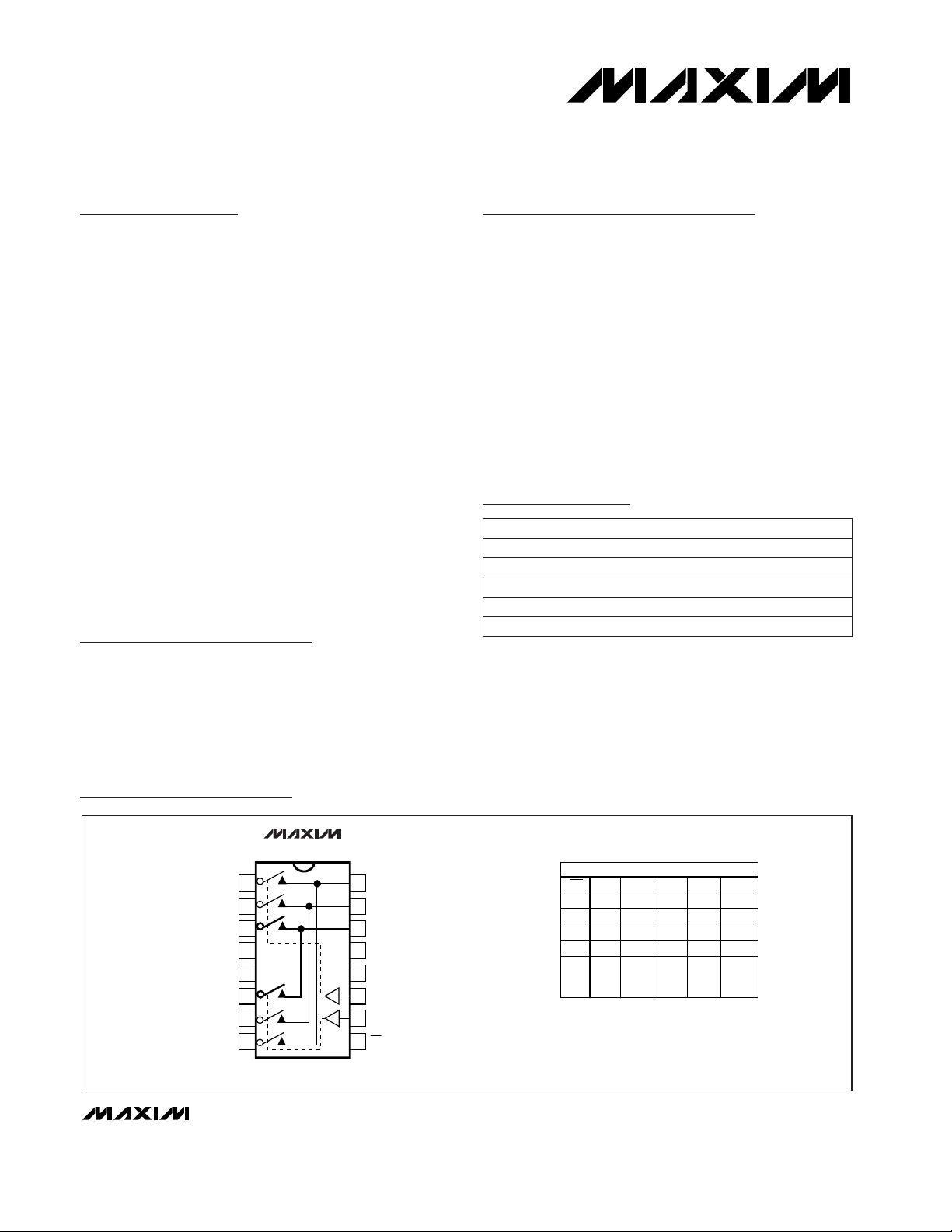
TOP VIEW
16
15
14
13
12
11
10
9
1
2
3
4
5
6
7
8
MAX4554
DIP/SO
COMG
COMS
COMF*
V+
VL
IN1
IN2
EN
V-
NOF1*
NOS1
NOG1
NOG2
NOS2
NOF2*
GND
MAX4554
NOTE: SWITCH POSITIONS SHOWN WITH IN_ = LOW
*INDICATES HIGH-CURRENT, LOW-RESISTANCE FORCE SWITCH
X = DON’T CARE
EN
IN1 IN2 COMG COMS COMF*
1
0
0
0
X
0
0
1
X
0
1
0
OFF
OFF
NOG2
NOG1
OFF
OFF
NOS2
NOS1
OFF
OFF
NOF2*
NOF1*
NOG1
&
NOG2
NOS1
&
NOS2
NOF1*
&
NOF2*
1
10
19-1358; Rev 0; 4/98
PART
MAX4554CPE
MAX4554CSE 0°C to +70°C
0°C to +70°C
TEMP. RANGE PIN-PACKAGE
16 Plastic DIP
16 Narrow SO
Ordering Information continued at end of data sheet.
*
Contact factory for availability.
Pin Configurations/Functional Diagrams/Truth Tables
Ordering Information
Rail-to-Rail is a registered trademark of Nippon Motorola Ltd.
MAX4554C/D
MAX4554EPE -40°C to +85°C
0°C to +70°C Dice*
16 Plastic DIP
MAX4554ESE -40°C to +85°C 16 Narrow SO
MAX4555/MAX4556 shown at end of data sheet.
MAX4554/MAX4555/MAX4556
Force-Sense Switches
2 _______________________________________________________________________________________
ABSOLUTE MAXIMUM RATINGS
ELECTRICAL CHARACTERISTICS—MAX4554 (+20V, -10V Supplies)
(V+ = +20V, V- = -10V, VL = 5V, GND = 0V, V
IN_H
= 2.4V, V
IN_L
= 0.8V, TA= T
MIN
to T
MAX
, unless otherwise noted. Typical values
are at T
A
= +25°C.)
Stresses beyond those listed under “Absolute Maximum Ratings” may cause permanent damage to the device. These are stress ratings only, and functional
operation of the device at these or any other conditions beyond those indicated in the operational sections of the specifications is not implied. Exposure to
absolute maximum rating conditions for extended periods may affect device reliability.
Note 1: Signals on analog or digital pins exceeding V+ or V- are clamped by internal diodes. Limit forward diode current to maxi-
mum current rating.
(Voltages referenced to GND)
V+...........................................................................-0.3V to +44V
V-............................................................................-25V to +0.3V
V+ to V-...................................................................-0.3V to +44V
All Other Pins (Note 1)..........................(V- - 0.3V) to (V+ + 0.3V)
Continuous Current into Force Terminals.......................±100mA
Continuous Current into Any Other Terminal....................±30mA
Peak Current into Force Terminals
(pulsed at 1ms, 10% duty cycle).................................±300mA
Peak Current into Any Other Terminal
(pulsed at 1ms, 10% duty cycle).................................±100mA
ESD per Method 3015.7 ..................................................>2000V
Continuous Power Dissipation (T
A
= +70°C)
Plastic DIP (derate 10.53mW/°C above +70°C) ...........842mW
Narrow SO (derate 8.7mW/°C above +70°C) ...............696mW
Operating Temperature Ranges
MAX455_C_ E......................................................0°C to +70°C
MAX455_E_ E ...................................................-40°C to +85°C
Storage Temperature Range.............................-65°C to +150°C
Lead Temperature (soldering, 10sec).............................+300°C
60Ω ANALOG SWITCH (SENSE-GUARD)
6Ω ANALOG SWITCH (FORCE)
+25°C
+25°C
C, E
+25°C
C, E
+25°C
3.5 6
On-Resistance Match
(Note 4)
0.4 1
∆R
ON
1.5
Ω
On-Resistance Flatness
(Note 5)
0.5 1.5
R
FLAT(ON)
2.0
Ω
NOF_ Off-Leakage Current
-0.25 0.03 0.25
V
COMF
= 10V, I
COMF
= 10mA
V
COMF
= +5V, 0V, -5V;
I
COMF
= 10mA
T
A
C, E
PARAMETER SYMBOL
MIN TYP MAX
(Note 2)
UNITS
C, E
On-Resistance R
ON
7
+25°C
C, E
+25°C
C, E
Analog Signal Range
V
COMF
,
V
NOF_
V- V+ V
34 60
On-Resistance R
ON
70
Ω
5 8
On-Resistance Match
(Note 4)
∆R
ON
10
Ω
V
COM_
= 10V, I
COM_
= 1mA
V
COM_
= 10V, I
COM_
= 1mA
C, E
+25°C
C, E
C, E
C, E
Ω
I
COMF(OFF)
-2.5 2.5
nA
COMF On-Leakage Current
-0.5 0.06 0.5
V
COMF
= 10V, I
COMF
= 10mA
I
COMF(ON)
-10 10
nA
Charge Injection Q 80 pC
CONDITIONS
Analog Signal Range
V
COMS
,
V
COMG
,
V
NOS_
,
V
NOG_
V- V+ V
V+ = 22V, V- = -11V,
V
COMF
= ±10V, V
NOF_
= 10V
V+ = 22V, V- = -11V,
V
COMF
= ±10V
V
COMF
= 0, Figure 13
(Note 3)
C, E
+25°C
COMF Off-Leakage Current
I
NOF_(OFF)
-2.5 2.5
(Note 3)
nA
-0.5 0.03 0.5
V+ = 22V, V- = -11V,
V
COMF
= ±10V, V
NOF_
= 10V
±
±
MAX4554/MAX4555/MAX4556
Force-Sense Switches
_______________________________________________________________________________________ 3
ELECTRICAL CHARACTERISTICS—MAX4554 (+20V, -10V Supplies) (continued)
(V+ = +20V, V- = -10V, VL = 5V, GND = 0V, V
IN_H
= 2.4V, V
IN_L
= 0.8V, TA= T
MIN
to T
MAX
, unless otherwise noted. Typical values
are at T
A
= +25°C.)
SWITCH DYNAMIC CHARACTERISTICS
LOGIC INPUT
+25°C
COMS, COMG
On-Capacitance
C
ON
30 pF
V
COMS, VCOMG
= GND; f = 1MHz;
Figure 14
+25°CCOMF On-Capacitance C
ON
130 pFV
COMF
= GND, f = 1MHz, Figure 14
+25°COff Isolation (Force) V
ISO
-30 dB
R
IN_
= 50Ω, R
OUT
= 50Ω, f = 1MHz,
V
COM_
= 100mV
RMS
, Figure 15
+25°C
C, E
170 275
Enable Time Off
+25°C
C, E
t
EN
350
375 500
ns
Enable Time On t
EN
600
ns
V
COM_
= 10V, Figure 11
V
COM_
= 10V, Figure 11
+25°C
C, E
130 300
Turn-Off Time
(Sense-Guard)
+25°C
C, E
t
OFF
350
130 300
ns
Turn-Off Time (Force) t
OFF
350
ns
V
COMS, VCOMG
= 10V; RL= 1kΩ;
Figure 10
V
COMF
= 3V, RL= 300Ω,
Figure 10
+25°C
C, E
150 300
Turn-On Time
(Sense-Guard)
t
ON
350
ns
V
COMS, VCOMG
= 10V; RL= 1kΩ;
Figure 10
+25°C
+25°C
COMS, COMG
Off-Capacitance
C
OFF
15 pF
Total Harmonic Distortion
(Force)
THD 0.007 %
V
COMS, VCOMG
= GND; f = 1MHz;
Figure 14
C, E
IN_, EN Input Current Logic
High or Low
I
IN_H
, I
IN_L
,
I
ENH
, I
ENL
-0.5 0.03 0.5 µAV
IN_
= VEN= 0 or VL
C, E
IN_, EN Input Logic
Threshold Low
V
IN_L
,
V
ENL
0.8 1.6 V
+25°C
C, E
+25°C
+25°C
+25°C
150 300
Turn-On Time (Force) t
ON
350
ns
NOF_ Off-Capacitance C
OFF
22 pF
NOS_, NOG_
Off-Capacitance
C
OFF
7 pF
COMF Off-Capacitance C
OFF
50 pF
V
COMF
= 3V, RL= 300Ω,
Figure 10
V
NOF
= GND, f = 1MHz, Figure 14
V
NOS_, VNOG_
= GND; f = 1MHz;
Figure 14
V
COMF
= GND, f = 1MHz, Figure 14
C, E
+25°C
C, E
+25°C
C, E
I
COMS(OFF)
,
I
COMG(OFF)
-2.5 2.5
nA
COMS, COMG On-Leakage
Current
-0.5 0.04 0.5
I
COMS(ON)
,
I
COMG(ON)
-5.0 5.0
nA
Charge Injection Q 6 pC
IN_, EN Input Logic
Threshold High
V
IN_H
,
V
ENH
1.6 2.4 V
V+ = 22V; V- = -11V; V
COM_
= ±10V;
V
NOS_, VNOG_
= ±10V
V+ = 22V, V- = -11V, V
COM_
= ±10V
V
COM_
= 0, Figure 13
C, E
+25°C
COMS, COMG Off-Leakage
Current
I
NOS_(OFF)
,
I
NOG_(OFF)
-2.5 2.5
nA
-0.25 0.02 0.25
V+ = 22V; V- = -11V; V
COM_
= ±10V;
V
NOS_, VNOG_
= ±10V
+25°C
C, E
+25°C
On-Resistance Flatness
(Note 5)
3.5 9
R
FLAT(ON)
10
Ω
NOS_, NOG_ Off-Leakage
Current
-0.25 0.02 0.25
V
COM_
= +5V, 0V, -5V;
I
COM_
= 10mA
T
A
PARAMETER SYMBOL
MIN TYP MAX
(Note 2)
UNITSCONDITIONS
SWITCH DYNAMIC CHARACTERISTICS
MAX4554/MAX4555/MAX4556
Force-Sense Switches
4 _______________________________________________________________________________________
ELECTRICAL CHARACTERISTICS—MAX4554 (+20V, -10V Supplies) (continued)
(V+ = +20V, V- = -10V, VL = 5V, GND = 0V, V
IN_H
= 2.4V, V
IN_L
= 0.8V, TA= T
MIN
to T
MAX
, unless otherwise noted. Typical values
are at T
A
= +25°C.)
ELECTRICAL CHARACTERISTICS—MAX4554 (±15V Supplies)
(V+ = +15V, V- = -15V, VL = 5V, GND = 0V, V
IN_H
= 2.4V, V
IN_L
= 0.8V, TA= T
MIN
to T
MAX
, unless otherwise noted. Typical values
are at T
A
= +25°C.)
POWER SUPPLY
+25°C
+25°C
C, E
+25°C
C, E
+25°C
-1.0 1.0
V- Supply Current
-1.0 1.0
I-
-5.0 5.0
µA
VL Supply Current
-1.0 1.0
I
L+
-5.0 5.0
µA
Ground Current
-1.0 1.0
V+ = 22V; V- = -11V;
V
EN, VIN_
= 0 or VL
V+ = 22V; V- = -11V;
V
EN, VIN_
= 0 or VL
T
A
C, E
PARAMETER SYMBOL
MIN TYP MAX
(Note 2)
UNITS
C, E
V+ Supply Current I+
-5.0 5.0
Power-Supply Range V+, VL, V-
±4.5 ±20 V
µA
V+ = 22V; V- = -11V;
V
EN, VIN_
= 0 or VL
CONDITIONS
C, E
I
GND
-5.0 5.0
VL ≥ 4.5V
µA
V+ = 22V; V- = -11V;
V
EN, VIN_
= 0 or VL
60Ω ANALOG SWITCH (SENSE-GUARD)
6Ω ANALOG SWITCH (FORCE)
+25°C
+25°C
C, E
+25°C
C, E
+25°C
4 6
On-Resistance Match
(Note 4)
0.5 1
∆R
ON
1.5
Ω
On-Resistance Flatness
(Note 5)
0.1 1
R
FLAT(ON)
1.5
Ω
NOF_ Off-Leakage Current
-0.25 0.03 0.25
V
COMF
= ±10V, I
COMF
= 10mA
V
COMF
= +5V, 0V, -5V;
I
COMF
= 10mA
T
A
C, E
PARAMETER SYMBOL
MIN TYP MAX
(Note 2)
UNITS
C, E
On-Resistance R
ON
7
+25°C
C, E
Analog Signal Range
V
COMF
,
V
NOF_
V- V+ V
38 60
On-Resistance R
ON
70
ΩV
COM_
= ±10V, I
COM_
= 1mA
C, E
+25°C
C, E
+25°C
C, E
Ω
I
COMF(OFF)
-5.0 5.0
nA
COMF On-Leakage Current
-0.5 0.06 0.5
V
COMF
= ±10V, I
COMF
= 10mA
I
COMF(ON)
-10 10
nA
Charge Injection Q 100 pC
CONDITIONS
Analog Signal Range
V
COMS
,
V
COMG
,
V
NOS_
,
V
NOG_
V- V+ V
V+ = 16.5V, V- = -16.5V,
V
COMF
= ±10V, V
NOF_
= 10V
V+ = 16.5V, V- = -16.5V,
V
COMF
= ±10V
V
COMF
= 0, Figure 13
(Note 3)
C, E
+25°C
COMF Off-Leakage Current
I
NOF_(OFF)
-2.5 2.5
(Note 3)
nA
-0.5 0.03 0.5
V+ = 16.5V, V- = -16.5V,
V
COMF
= ±10V, V
NOF_
= 10V
±
±
MAX4554/MAX4555/MAX4556
Force-Sense Switches
_______________________________________________________________________________________ 5
ELECTRICAL CHARACTERISTICS—MAX4554 (±15V Supplies) (continued)
(V+ = +15V, V- = -15V, VL = 5V, GND = 0V, V
IN_H
= 2.4V, V
IN_L
= 0.8V, TA= T
MIN
to T
MAX
, unless otherwise noted. Typical values
are at T
A
= +25°C.)
SWITCH DYNAMIC CHARACTERISTICS
LOGIC INPUT
+25°C
C, E
On-Resistance Flatness
(Note 5)
1.5 5
R
FLAT(ON)
6
ΩV
COM_
= +5V, 0V, -5V; I
COM_
= 1mA
+25°C
C, E
+25°C
On-Resistance Match
(Note 4)
5 9
∆R
ON
10
Ω
NOS_, NOG Off-Leakage
Current
-0.25 0.01 0.25
V
COM_
= ±10V, I
COM_
= 1mA
T
A
+25°C
C, E
170 300
Enable Time Off
+25°C
C, E
t
EN
400
310 500
ns
Enable Time On t
EN
600
ns
V
COM_
= ±10V, RL= 300Ω,
Figure 11
PARAMETER SYMBOL
MIN TYP MAX
(Note 2)
UNITS
V
COM_
= ±10V, RL= 300Ω,
Figure 11
+25°C
C, E
135 225
Turn-Off Time
(Sense-Guard)
+25°C
C, E
t
OFF
275
170 275
ns
Turn-Off Time (Force) t
OFF
325
ns
V
COM_
= ±10V, RL= 1kΩ,
Figure 10
V
COM_
= ±10V, RL= 300Ω,
Figure 10
+25°C
C, E
135 225
Turn-On Time
(Sense-Guard)
+25°C
COMS, COMG
Off-Capacitance
C
OFF
9 pF
+25°C
C, E
+25°C
+25°C
V
COMS_, VCOMG
_= GND; f = 1MHz;
Figure 14
C, E
IN_, EN Input Current Logic
High or Low
+25°C
t
ON
275
135 275
ns
Turn-On Time (Force) t
ON
325
ns
NOF_ Off-Capacitance C
OFF
22 pF
NOS_, NOG_
Off-Capacitance
C
OFF
9 pF
COMF Off-Capacitance C
OFF
29 pF
V
COM_
= ±10V, RL= 1kΩ,
Figure 10
V
COM_
= ±10V, RL= 300Ω,
Figure 10
V
NOF
= GND, f = 1MHz, Figure 14
V
NOS_, VNOG_
= GND; f = 1MHz;
Figure 14
C, E
+25°C
C, E
+25°C
C, E
I
IN_H
, I
IN_L
,
I
ENH
, I
ENL
I
COMS(OFF)
,
I
COMG(OFF)
-2.5 2.5
nA
COMS, COMG On-Leakage
Current
-0.5 0.03 0.5
-0.5 0.02 0.5
µAVEN= 0 or VL
I
COMS(ON)
,
I
COMG(ON)
-5.0 5.0
nA
Charge Injection Q 4 pC
CONDITIONS
IN_, EN Input Logic
Threshold High
V
IN_H
,
V
ENH
1.6 2.4 V
V+ = 16.5V; V- = -16.5V;
V
COM_
= ±10V; V
NOS_, VNOG_
= 10V
C, E
V+ = 16.5V, V- = -16.5V,
V
COM_
= ±10V
V
COM_
= 0, Figure 13
C, E
+25°C
COMS, COMG Off-Leakage
Current
V
COMF
= GND, f = 1MHz, Figure 14
I
NOS_(OFF)
,
I
NOG_(OFF)
IN_, EN Input Logic
Threshold Low
-2.5 2.5
V
IN_L
,
V
ENL
nA
0.8 1.6
-0.25 0.01 0.25
V
V+ = 16.5V; V- = -16.5V;
V
COM_
= ±10V; V
NOS_, VNOG_
= 10V
±
±
MAX4554/MAX4555/MAX4556
Force-Sense Switches
6 _______________________________________________________________________________________
ELECTRICAL CHARACTERISTICS—MAX4554 (±15V Supplies) (continued)
(V+ = +15V, V- = -15V, VL = 5V, GND = 0V, V
IN_H
= 2.4V, V
IN_L
= 0.8V, TA= T
MIN
to T
MAX
, unless otherwise noted. Typical values
are at T
A
= +25°C.)
ELECTRICAL CHARACTERISTICS—MAX4555 (±15V Supplies)
(V+ = +15V, V- = -15V, VL = 5V, GND = 0V, V
IN_H
= 2.4V, V
IN_L
= 0.8V, TA= T
MIN
to T
MAX
, unless otherwise noted. Typical values
are at T
A
= +25°C.)
V+ = 16.5V, V- = -16.5V,
V
COM_
= ±10V, V
NO_
= 10V
-0.5 0.03 0.5
nA
(Note 3)
-2.5 2.5
I
NC_(OFF)
COM_ Off-Leakage Current
+25°C
C, E
V
COM_
= 0, Figure 13
V+ = 16.5V, V- = -16.5V,
V
COM_
= ±10V
V+ = 16.5V, V- = -16.5V,
V
COM_
= ±10V, V
NO_
= 10V
CONDITIONS
pC100QCharge Injection
nA
-10 10
I
COM_(ON)
V
COM_
= ±10V, I
COM_
= 10mA
-0.5 0.06 0.5
COM_ On-Leakage Current
nA
-5.0 5.0
I
COM_(OFF)
Ω
+25°C
C, E
+25°C
C, E
VV- V+V
COM_
, V
NO_
Analog Signal Range
7
R
ON
On-Resistance
C, E
UNITS
MIN TYP MAX
(Note 2)
SYMBOLPARAMETER
C, E
T
A
V
COM_
= +5V, 0V, -5V;
I
COM_
= 10mA
V
COM_
= ±10V, I
COM_
= 10mA
-0.25 0.03 0.25
NC_ Off-Leakage Current
Ω
1.5
R
FLAT(ON)
0.05 1
On-Resistance Flatness
(Note 5)
Ω
1.5
∆R
ON
0.3 1
On-Resistance Match
(Note 4)
3.8 6
+25°C
C, E
+25°C
C, E
+25°C
+25°C
6Ω ANALOG SWITCH (FORCE)
±
±
POWER SUPPLY
µA
-5.0 5.0C, E
V+ = 16.5V; V- = -16.5V;
V
EN, VIN_
= 0 or V+
µA
-5.0 5.0C, E
V+ = 16.5V; V- = -16.5V;
V
EN, VIN_
= 0 or V+
I
L+
VL Supply Current
I
GND
-1.0 0.001 1.0+25°C
Ground Current
-1.0 1.0+25°C
µA
-5.0 5.0C, E
V+ = 16.5V; V- = -16.5V;
V
EN, VIN_
= 0 or V+
I-V- Supply Current
-1.0 0.001 1.0+25°C
µA
-5.0 5.0C, E
V+ = 16.5V; V- = -16.5V;
V
EN, VIN_
= 0 or V+
I+V+ Supply Current
-1.0 0.001 1.0+25°C
V±4.5 ±20
C, EVL ≥ 4.5VV+, VL, V-Power-Supply Range
+25°CCOMF On-Capacitance C
ON
107 pF
V
COMF
= GND, f = 1MHz,
Figure 14
T
A
+25°COff Isolation (Force) V
ISO
-30 dB
R
IN_
= 50Ω, R
OUT
= 50Ω, f = 1MHz,
V
COM_
= 100mV
RMS
, Figure 15
PARAMETER SYMBOL
MIN TYP MAX
(Note 2)
UNITS
+25°C
COMS, COMG
On-Capacitance
C
ON
29 pF
V
COMS, VCOMG_
= GND; f = 1MHz;
Figure 14
CONDITIONS
+25°C
Total Harmonic Distortion
(Force)
THD 0.007 %
MAX4554/MAX4555/MAX4556
Force-Sense Switches
_______________________________________________________________________________________ 7
ELECTRICAL CHARACTERISTICS—MAX4555 (±15V Supplies) (continued)
(V+ = +15V, V- = -15V, VL = 5V, GND = 0V, V
IN_H
= 2.4V, V
IN_L
= 0.8V, TA= T
MIN
to T
MAX
, unless otherwise noted. Typical values
are at T
A
= +25°C.)
V+ = 16.5V, V- = -16.5V,
V
COM_
= ±10V, V
NO_
= 10V
-0.3 0.01 0.3
nA
(Note 3)
-2.5 2.5
I
NC_(OFF)
COM_ Off-Leakage Current
+25°C
C, E
V
COM_
= 0, Figure 13
V+ = 16.5V, V- = -16.5V,
V
NC_
= ±10V
V+ = 16.5V, V- = -16.5V,
V
COM_
= ±10V, V
NO_
= 10V
CONDITIONS
pC4QCharge Injection
nA
-5.0 5.0
I
NC_(ON)
V
COM_
= ±10V, I
COM_
= 10mA
-0.6 0.02 0.6
COM_ On-Leakage Current
nA
-2.5 2.5
I
COM_(OFF)
Ω
+25°C
C, E
+25°C
C, E
VV- V+V
COM_
, V
NO_
Analog Signal Range
45
R
ON
On-Resistance
C, E
UNITS
MIN TYP MAX
(Note 2)
SYMBOLPARAMETER
C, E
T
A
V
COM_
= +5V, 0V, -5V;
I
COM_
= 10mA
V
COM_
= ±10V, I
COM_
= 10mA
-0.3 0.01 0.3
NC_ Off-Leakage Current
Ω
6
R
FLAT(ON)
0.6 5
On-Resistance Flatness
(Note 5)
Ω
5
∆R
ON
0.6 4
On-Resistance Match
(Note 4)
15 30
+25°C
C, E
+25°C
C, E
+25°C
+25°C
V1.6 2.4V
IN_H
IN_ Input Logic Threshold
High
C, E
V0.8 1.6V
IN_L
IN_ Input Logic Threshold
Low
C, E
V
IN_
= 0.8V or 2.4V µA-0.5 0.03 0.5
I
IN_H
,
I
IN_L
IN_ Input Current Logic
High or Low
C, E
155 275+25°C
V
COM_
= ±3V, RL= 300Ω,
Figure 10
ns
325
t
ON
Turn-On Time (Force)
C, E
125 225+25°C
V
COM_
= ±10V, RL= 1kΩ,
Figure 10
ns
275
t
ON
Turn-On Time
(Sense-Guard)
C, E
125 225+25°C
190 275
V
COM_
= ±10V, RL= 1kΩ,
Figure 10
ns
+25°C
V
COM_
= ±3V, RL= 300Ω,
Figure 10
ns
325
t
OFF
Turn-Off Time (Force)
C, E
275
t
OFF
Turn-Off Time
(Sense-Guard)
C, E
29+25°C
V
COM_, VNO_
= GND; f = 1MHz;
Figure 14
pF
9
C
OFF
COM_ Off-Capacitance
(Force)
+25°C
COM_ On-Capacitance
(Sense-Guard)
C
ON
V
COM_, VNO_
= GND; f = 1MHz;
Figure 14
pF
107+25°C
V
COM_, VNO_
= GND; f = 1MHz;
Figure 14
pF
29
C
ON
COM_ On-Capacitance
(Force)
+25°C
COM_ Off-Capacitance
(Sense-Guard)
C
OFF
V
COM_, VNO_
= GND; f = 1MHz;
Figure 14
pF
30Ω ANALOG SWITCH (SENSE-GUARD)
LOGIC INPUT
SWITCH DYNAMIC CHARACTERISTICS
±
±
MAX4554/MAX4555/MAX4556
Force-Sense Switches
8 _______________________________________________________________________________________
ELECTRICAL CHARACTERISTICS—MAX4555 (±15V Supplies) (continued)
(V+ = +15V, V- = -15V, VL = 5V, GND = 0V, V
IN_H
= 2.4V, V
IN_L
= 0.8V, TA= T
MIN
to T
MAX
, unless otherwise noted. Typical values
are at T
A
= +25°C.)
ELECTRICAL CHARACTERISTICS—MAX4556 (±15V Supplies)
(V+ = +15V, V- = -15V, VL = 5V, GND = 0V, V
IN_H
= 2.4V, V
IN_L
= 0.8V, TA= T
MIN
to T
MAX
, unless otherwise noted. Typical values
are at T
A
= +25°C.)
6Ω ANALOG SWITCH (FORCE)
+25°C
+25°C
C, E
+25°C
C, E
+25°C
3.8 6
On-Resistance Match
(Note 4)
0.3 1
∆R
ON
1.5
Ω
On-Resistance Flatness
(Note 5)
0.05 1
R
FLAT(ON)
1.5
Ω
NO1, NC1 Off-Leakage
Current
-0.25 0.03 0.25
V
COM1
= ±10V, I
COM1
= 10mA
V
COM1
= +5V, 0V, -5V;
I
COM1
= 10mA
T
A
C, E
PARAMETER SYMBOL
MIN TYP MAX
(Note 2)
UNITS
C, E
On-Resistance R
ON
7
Analog Signal Range
V
COM1
,
V
NO1
, V
NC1
V- V+ V
C, E
+25°C
C, E
+25°C
Ω
I
COM1(OFF)
-5.0 5.0
nA
COM1 On-Leakage Current
-0.5 0.06 0.5
V
COM1
= ±10V, I
COM1
= 10mA
I
COM1(ON)
-10 10
nA
Charge Injection Q 100 pC
CONDITIONS
V+ = 16.5V, V- = -16.5V,
V
COM1
= ±10V, V
NO1
= 10V
V+ = 16.5V, V- = -16.5V,
V
COM1
= ±10V
V
COM1
= 0, Figure 13
C, E
+25°C
COM1 Off-Leakage Current
I
NO1(OFF)
,
I
NC1(OFF)
-2.5 2.5
(Note 3)
nA
-0.5 0.03 0.5
V+ = 16.5V; V- = -16.5V;
V
COM1
= ±10V; V
NO1, VNC1
= 10V
±
±
Power-Supply Range V+, VL, V- C, E ±4.5 ±20 V
+25°C -1.0 0.001 1.0
V- Supply Current
+25°C -1.0 0.001 1.0
I-
V+ Supply Current I+
V+ = 16.5V; V- = -16.5V;
V
EN, VIN_
= 0 or V+
C, E -5.0 5.0
µA
CONDITIONS
V+ = 16.5V; V- = -16.5V;
V
EN, VIN_
= 0 or V+
C, E -5.0 5.0
µA
+25°C -1.0 0.001 1.0
Ground Current
+25°C -1.0 0.001 1.0
I
GND
VL Supply Current I
L+
V+ = 16.5V; V- = -16.5V;
V
EN, VIN_
= 0 or V+
C, E -5.0 5.0
µA
V+ = 16.5V; V- = -16.5V;
V
EN, VIN_
= 0 or V+
C, E -5.0 5.0
µA
%0.007THD
Total Harmonic Distortion
(Force)
+25°C
UNITS
MIN TYP MAX
(Note 2)
SYMBOLPARAMETER
R
IN
= 50Ω, R
OUT
= 50Ω, f = 1MHz,
V
COM_
= 100mV
RMS
, Figure 15
dB-38V
ISO
Off Isolation (Force)
(Note 6)
+25°C
T
A
V
COM_, VNO_
= GND; f = 1MHz;
Figure 14
pF9C
OFF
NC_ Off-Capacitance
(Sense-Guard)
+25°C
V
COM_, VNO_
= GND; f = 1MHz;
Figure 14
pF22C
OFF
NC_ Off-Capacitance
(Force)
+25°C
POWER SUPPLY
MAX4554/MAX4555/MAX4556
Force-Sense Switches
_______________________________________________________________________________________ 9
ELECTRICAL CHARACTERISTICS—MAX4556 (±15V Supplies) (continued)
(V+ = +15V, V- = -15V, VL = 5V, GND = 0V, V
IN_H
= 2.4V, V
IN_L
= 0.8V, TA= T
MIN
to T
MAX
, unless otherwise noted. Typical values
are at T
A
= +25°C.)
SWITCH DYNAMIC CHARACTERISTICS
LOGIC INPUT
60Ω ANALOG SWITCH (SENSE-GUARD)
dB
R
IN
= 50Ω, R
OUT
= 50Ω, f = 1MHz,
V
COM_
= 100mV
RMS
, Figure 15
V
ISO
Off Isolation (Force) +25°C -30
%THD
Total Harmonic Distortion
(Force)
+25°C 0.007
+25°C
+25°C
C, E
+25°C
C, E
+25°C
36 60
On-Resistance Match
(Note 4)
5 9
∆R
ON
10
Ω
On-Resistance Flatness
(Note 5)
0.6 5
R
FLAT(ON)
6
Ω
NO_, NC Off-Leakage
Current
-0.25 0.01 0.25
V
COM_
= ±10V, I
COM_
= 10mA
V
COM_
= +5V, 0V, -5V;
I
COM_
= 10mA
T
A
pF
V
COM_
= GND, f = 1MHz,
Figure 14
C
ON
C, E
COM_ On-Capacitance
(Sense-Guard)
+25°C
NO_, NC_ Off-Capacitance
(Sense-Guard)
C
OFF
30
pF
PARAMETER SYMBOL
MIN TYP MAX
(Note 2)
UNITS
V
NO_, VNC_
= GND; f = 1MHz;
Figure 14
+25°C 7
pF
V
COM1
= GND, f = 1MHz,
Figure 14
C
ON
COM1 On-Capacitance
(Force)
+25°C
NO1, NC1 Off-Capacitance
(Force)
C
OFF
137
pF
V
NO1, VNC1
= GND; f = 1MHz;
Figure 14
+25°C 21
Break-Before-Make Time t
BBM
C, E
On-Resistance R
ON
70
nsV
COM_
= ±10V, RL= 1kΩ, Figure 12 +25°C
Analog Signal Range
V
COM_
,
V
NO_
, V
NC_
V- V+ V
1 15
C, E
Transition Time
(Sense-Guard)
t
TRANS
275
C, E
Transition Time (Force) t
TRANS
300
ns
V
COM_
= ±10V, RL= 300Ω,
Figure 10
+25°C
ns
V
COM_
= ±10V, RL= 1kΩ,
Figure 10
150 250
+25°C 125 225
C, E
IN_ Input Current Logic
High or Low
I
IN_H
,
I
IN_L
-0.5 0.03 0.5 µA
C, E
+25°C
C, E
+25°C
V
IN_
= 0 or VL
C, E
Ω
I
COM_(OFF)
-2.5 2.5
nA
COM_ On-Leakage Current
IN_ Input Logic Threshold
Low
-0.5 0.02 0.5
V
IN_L
V
COM_
= ±10V, I
COM_
= 10mA
I
COM_(ON)
-5.0 5.0
nA
Charge Injection Q 5 pC
0.8 1.6 V
C, E
CONDITIONS
IN_ Input Logic Threshold
High
V
IN_H
1.6 2.4 V
V+ = 16.5V; V- = -16.5V;
V
COM_
= ±10V; V
NO_, VNC_
= 10V
V+ = 16.5V, V- = -16.5V,
V
COM_
= ±10V
V
COM_
= 0, Figure 13
C, E
+25°C
COM_ Off-Leakage Current
I
NO_(OFF)
,
I
NC_(OFF)
-2.5 2.5
(Note 3)
nA
-0.25 0.01 0.25
V+ = 16.5V; V- = -16.5V;
V
COM_
= ±10V; V
NO_, VNC_
= 10V
±
±

MAX4554/MAX4555/MAX4556
Force-Sense Switches
10 ______________________________________________________________________________________
ELECTRICAL CHARACTERISTICS—MAX4556 (±15V Supplies) (continued)
(V+ = +15V, V- = -15V, VL = 5V, GND = 0V, V
IN_H
= 2.4V, V
IN_L
= 0.8V, TA= T
MIN
to T
MAX
, unless otherwise noted. Typical values
are at T
A
= +25°C.)
Note 2: The algebraic convention is used in this data sheet; the most negative value is shown in the minimum column.
Note 3: Guaranteed by design.
Note 4: ∆R
ON
= ∆R
ON(MAX)
- ∆R
ON(MIN)
.
Note 5: Resistance flatness is defined as the difference between the maximum and the minimum value of on-resistance as
measured over the specified analog signal range.
POWER SUPPLY
T
A
PARAMETER SYMBOL
MIN TYP MAX
(Note 2)
UNITS
µA
-5.0 5.0C, E
V+ = 16.5V, V- = -16.5V,
V
IN_
= 0 or VL
µA
-5.0 5.0C, E
V+ = 16.5V, V- = -16.5V,
V
IN_
= 0 or VL
I
L+
VL Supply Current
I
GND
-1.0 0.001 1.0+25°C
Ground Current
-1.0 0.001 1.0+25°C
µA
-5.0 5.0C, E
V+ = 16.5V, V- = -16.5V,
V
IN_
= 0 or VL
CONDITIONS
µA
-5.0 5.0C, E
V+ = 16.5V, V- = -16.5V,
V
IN_
= 0 or VL
I+V+ Supply Current
I-
-1.0 0.001 1.0+25°C
V- Supply Current
-1.0 0.001 1.0+25°C
V±4.5 ±20
C, EVL ≥ 4.5VV+, VL, V-Power-Supply Range

MAX4554/MAX4555/MAX4556
Force-Sense Switches
______________________________________________________________________________________
11
0
5
10
15
20
25
30
35
40
-15 -5-10 0 5 10 15
SWITCH ON-RESISTANCE vs. V
COM
(DUAL SUPPLIES)
MAX4554/5/6-01
V
COM
(V)
SWITCH ON-RESISTANCE (Ω)
MAX4554/MAX4556
SENSE & GUARD
MAX4555 SENSE
FORCE
0
2
1
4
3
5
6
-10 0 5-5 10 15 20
MAX4554
FORCE SWITCH ON-RESISTANCE
vs. V
COM
AND TEMPERATURE
MAX4554/5/6-02
V
COM
(V)
R
DS(ON)
(Ω)
TA = +85°C
TA = +25°C
TA = -40°C
10
25
20
15
30
35
40
45
50
55
60
-15 -5-10 0 5 10 15
SENSE/GUARD SWITCH ON-RESISTANCE
vs. V
COM
AND TEMPERATURE
MAX4554/5/6-03
V
COM
(V)
R
DS(ON)
(Ω)
TA = +85°C
TA = +25°C
TA = -40°C
100
1
0 1 32 4 6 8 12 145 7 9 111013 15
SWITCH ON-RESISTANCE vs. V
COM
(SINGLE +15V SUPPLY)
MAX4554/5/6-04
V
COM
(V)
SWITCH ON-RESISTANCE (Ω)
10
MAX4554/MAX4556
SENSE & GUARD
MAX4555 SENSE
FORCE
-40
0
-20
40
20
80
60
100
-10 0 5-5 10 15 20
MAX4554
CHARGE INJECTION vs. V
COM
(+20V, -10V SUPPLIES)
MAX4554/5/6-07
V
COM
(V)
Q (pC)
SENSE & GUARD
FORCE
100
10
0.0001
-50 125
ON-LEAKAGE CURRENT
vs. TEMPERATURE
1
MAX4554/5/6-05
TEMPERATURE (°C)
ON-LEAKAGE (nA)
25
0.01
0.001
-25 0 75
0.1
50
100
V+ = 15V,
V- = -15V,
V
COM
= 10V
±
FORCE
SENSE & GUARD
100
10
0.0001
-50 125
OFF-LEAKAGE CURRENT
vs. TEMPERATURE
1
MAX4554/5/6-06
TEMPERATURE (°C)
OFF-LEAKAGE (nA)
25
0.01
0.001
-25 0 75
0.1
50
100
V+ = 15V,
V- = -15V,
V
NC
OR VNO = ±10V
V
COM
= 10V
±
FORCE
SENSE & GUARD
__________________________________________Typical Operating Characteristics
(V+ = +15V, V- = -15V, GND = 0V, TA= +25°C, unless otherwise noted.)

MAX4554/MAX4555/MAX4556
Force-Sense Switches
12 ______________________________________________________________________________________
____________________________________Typical Operating Characteristics (continued)
(V+ = +15V, V- = -15V, GND = 0V, TA= +25°C, unless otherwise noted.)
-40
0
-20
40
20
80
60
100
-15 -5 0-10 5 10 15
MAX4555/MAX4556
CHARGE INJECTION vs. V
COM
(+15V SUPPLIES)
MAX4554/5/6-08
V
COM
(V)
Q (pC)
SENSE & GUARD
FORCE
0
150
100
50
200
250
300
350
400
450
500
-40 10 35 60-15 85
MAX4554
ON/OFF/ENABLE TIMES vs.
TEMPERATURE (+20V, -10V SUPPLIES)
MAX4554/5/6-09
TEMPERATURE (°C)
TIME (ns)
t
EN(ON)
t
EN(OFF)
t
ON
t
OFF
0
60
40
20
80
100
120
140
160
180
-40 -15 10 35 60 85
MAX4555/4556
ON/OFF/TRANSITION TIMES vs.
TEMPERATURE (+20V/-10V SUPPLIES)
MAX4554/5/6-10
TEMPERATURE (°C)
TIME (ns)
MAX4556 t
TRANS
MAX4555 tON/t
OFF
100
10
0.0001
-55
-75 100
1
MAX4554/5/6-11
TEMPERATURE (°C)
I+, I-, I
L
(µA)
0.01
0.001
-50
-25 0 75
50
0.1
25
85
A: I+ = 16.5V
B: I- = -16.5V
C: I
L
= 5.5V
SUPPLY CURRENT
vs. TEMPERATURE
A
B
C
100
0.001
FORCE SWITCH TOTAL HARMONIC
DISTORTION vs. FREQUENCY
0.01
MAX4554/5/6-14
FREQUENCY (Hz)
THD (%)
0.1
1
10
10 1k 10k100 100k
V+ = +15V
V- = -15V
5Vp-p, 600Ω IN & OUT
0
2
1
4
3
5
6
0 105 15 20 25
LOGIC-LEVEL THRESHOLD
vs. LOAD VOLTAGE
MAX4554/5/6-12
VL (V)
LOGIC-LEVEL THRESHOLD (V)
0
-120
0.1 10 1001 1000
FORCE SWITCH FREQUENCY RESPONSE
-40
-50
-60
-70
-80
-90
-100
-110
MAX4554/5/6-13
FREQUENCY (MHz)
SWITCH LOSS (dB)
PHASE (degrees)
-30
-20
-10
180
-180
60
30
0
-30
-60
-90
-120
-150
90
120
150
ON LOSS
OFF LOSS
ON PHASE

MAX4554/MAX4555/MAX4556
Force-Sense Switches
______________________________________________________________________________________ 13
Pin Description
Analog Guard Channel 1 Normally Open Terminal—1
Analog Signal Normally Open Terminals——
Analog Signal Common Terminals. COM2 and COM3 are low-resistance (force) switches on the MAX4555. COM1 is a low-resistance
(force) switch on the MAX4556.
2, 15*,
10*, 7
—
Analog Sense Channel 1 Normally Open Terminal—2
Analog Signal Normally Closed Pins. NC2 and NC3 are low-resistance
(force) switches.
3, 14, 11, 6—
Negative Analog Supply Voltage Input. Connect to GND for singlesupply operation.
44
Analog Force Signal Normally Open Terminal ——
Analog Force Channel 1 Normally Open Terminal—3*
Analog Force Channel 2 Normally Open Terminal—6*
Analog Sense Channel 2 Normally Open Terminal—7
Analog Force Signal Normally Closed Terminal——
Analog Guard Channel 2 Normally Open Terminal—8
Logic-Level Digital Inputs. See
Truth Tables.
1, 16, 9, 811, 10
Enable Logic-Level Digital Input. Connect to GND to enable all switches.—9
Analog Signal Normally Closed Terminal——
Ground. Connect to digital ground. (Analog signals have no ground
reference; they are limited to V+ and V-.)
55
Logic-Level Positive Supply Input. Connect to logic (+5V) supply. Can
be connected to V+ for single-supply operation.
1212
Analog Force Channel Common Terminal—14*
Analog Guard Channel Common Terminal—16
Analog Sense Channel Common Terminal—15
Positive Analog Supply Voltage Input. Internally connected to substrate.
1313
1, 2
14*, 15, 16
—
—
4
3*
—
—
—
6*
—
9, 10, 11
—
—
7, 8
5
12
—
—
—
13
NO3, NO2
COM1, COM2
COM3, COM4
NOS1
NC1, NC2,
NC3, NC4
V-
NO1*
NOF1*
NOF2*
NOS2
NC1*
NOG2
IN1, IN2,
IN3, IN4
NOG1
EN
NC2, NC3
GND
VL
COMF*
COMG
COMS
V+
NAME FUNCTION
PIN
MAX4554 MAX4555 MAX4556
* Indicates high-current, low-resistance (force) switch terminal.
Note: NO_, NC_, and COM_ pins are identical and interchangeable. Any may be considered as an input or output; signals pass
equally well in either direction.

MAX4554/MAX4555/MAX4556
Force-Sense Switches
14 ______________________________________________________________________________________
______________Force-Sense Philosophy
When a precise voltage must be applied to a load that
draws appreciable current, the resistance of the conductors connecting the source and the load can
degrade the load voltage. The resistance of the conductors forms a voltage divider with the load, so that
the load voltage is lower than the source voltage. The
greater the distance between the source and the load,
and the greater the current or conductor resistance, the
greater the degradation. The resulting signal reduction
can be overcome and the signal at the load guaranteed
by using a 4-wire technique known as Kelvin sensing,
or force-sense.
The basic idea behind the force-sense philosophy is to
use four wires, forcing a voltage or current through two
high-current wires to the load, and measuring (sensing)
the voltage with two separate wires that carry very low
or negligible current. One of two basic configurations is
used, depending on whether or not feedback is employed:
1) The sensed voltage can be completely independent
of the forced voltage or current, as in the case of a
4-wire ohmmeter, where a constant current is forced
through one pair of wires and the voltage at the
resistor is measured by another pair.
2) The sensed voltage can be part of a feedback circuit to force the load voltage to the desired value,
as in the case of a 4-wire power supply. (In rare
cases, this method is also used to measure resistance; the source is forced to produce a desired
voltage in the resistor, and the source current
required to achieve this voltage is measured.)
In all cases, the resistance of the high-current conductors can be ignored and the sensed voltage is an accurate measure of the load (or resistor’s) voltage, despite
appreciable voltage loss in the wires connecting the
source and load.
There are two limitations to this scheme. First, the maximum source voltage (compliance) must be able to
overcome the combined voltage loss of the load and
the connecting wires. In other words, the conductors in
the force circuit can have significant resistance, but
there is a limit. Second, the impedance of the sensing
circuit (typically a voltmeter, A/D converter, or feedback
amplifier) must be very high compared to the load
resistance and the sense wire resistance. These limitations are usually simple to overcome. The source compliance is usually required to be only a volt more than
the load voltage, and the sense circuit usually has a
multimegohm impedance. Typical 4-wire force-sense
configurations are shown in Figure 1.
VOLTAGE
MEASUREMENT
MEASURED
RESISTANCE
CURRENT SOURCE
FORCE CURRENT
FORCE CURRENT
SENSE VOLTAGE
SENSE VOLTAGE
WIRE AND TERMINAL RESISTANCE
4-WIRE RESISTANCE MEASUREMENT (CONSTANT CURRENT)
VOLTAGE
MEASUREMENT
MEASURED
RESISTANCE
VOLTAGE SOURCE
FORCE VOLTAGE
FORCE VOLTAGE
SENSE VOLTAGE
SENSE VOLTAGE
WIRE AND TERMINAL RESISTANCE
4-WIRE RESISTANCE MEASUREMENT (CONSTANT VOLTAGE)
VOLTAGE
MEASUREMENT
LOAD
CURRENT SOURCE
FORCE CURRENT
FORCE CURRENT
SENSE VOLTAGE
SENSE VOLTAGE
WIRE AND TERMINAL RESISTANCE
4-WIRE POWER SUPPLY
FEEDBACK
V
V
V
V
FEEDBACK
ARROWS INDICATE SIGNAL DIRECTION, NOT POLARITY
Figure 1. 4-Wire Force-Sense Measurements

__________________Guard Philosophy
When measuring a precise voltage from a high-resistance source, or when measuring a very small current
or forcing it into a load, unwanted leakage currents can
degrade the results. These leakage currents may exist
in the insulation of wires connecting the source and the
measuring device. Higher source voltages, higher
source impedances, longer wires, lower currents, and
higher temperatures further degrade the measurement.
The effect has both DC and low-frequency AC components; AC signals are generally capacitively coupled
into the high-impedance source and wiring. The AC
and DC effects are hard to separate, and are generally
grouped under the designation “low-frequency noise.”
This signal degradation can be overcome and the measured signal guaranteed by using a 3-wire technique
known as guarding.
A “guard,” “guard channel,” or “driven guard” is formed
by adding a third wire to a 2-wire measurement. It consists of a physical barrier (generally the surrounding
shield of a coaxial cable) that is actively forced to the
same voltage as is being measured on its inner conductor. The forcing of the driven guard is from the output of
a low-impedance buffer amplifier whose high-impedance input is connected to the source. The idea is not
just to buffer or shield the signal with a low-impedance
source but, by forcing the shield to the same potential
as the signal, to also force the leakage currents
between the signal and the outside world to extremely
small values. Any unwanted leakage current from the
source must first go through the coaxial-cable insulation
to the shield. Since the shield is at the same potential,
there is virtually no unwanted leakage current, regard less of the insulation resistance. The shield itself can
have significant leakage currents to the outside world,
but it is separated from the measured signal.
The physical positioning of the guard around the signal
is extremely important in maintaining low leakage.
Since the guard can be at potentials far from ground,
conventional coaxial cable is often replaced by triaxial
cable (i.e., cable with a center conductor and two separate inner and outer shields). The signal is the center
conductor, the inner shield is the guard, and the outer
shield is the chassis ground. The outer shield isolates
the inner driven guard from ground, physically protects
the driven guard, and acts as a secondary Faraday
shield for external noise.
The physical guard must be maintained continuously
from the source to the measuring device, including
paths on printed circuit boards, where the guard
becomes extra traces surrounding the signal traces on
both sides (and above and below the signal traces on
multilevel boards.) This is one case where a ground
plane is
not
appropriate. In extreme cases, such as
with nano-voltmeters and femto-ammeters, printed circuit boards cannot be adequately shielded and are
eliminated from the guarded signal paths altogether.
Figure 2 shows both the basic 3-wire guarded measurement and a 5-wire variation, used for balanced signals that are elevated from ground potential. The 5-wire
configuration is really two 3-wire circuits sharing a common ground. Figure 2 also shows the configuration
using triaxial cable.
____Force-Sense-Guard Philosophy
Force-sense measurements are combined with guarded measurements when a wide range of voltages and
currents are encountered, or when voltage and current
must be accurately measured or controlled simultaneously. This frequently occurs in automatic test equipment (ATE) and in some critical physical or chemical
sensor applications where voltage and/or current measurements can span many decades. Two techniques
are used: 8-wire and 12-wire.
8-Wire Measurements
Figure 3 shows an 8-wire guarded force-sense power
supply. A precise voltage is forced to the load, and
load current is sensed without interacting with the output voltage, and without unwanted leakage currents.
Separate twin-axial, or “twinax” cable is used for each
of the positive and negative wires. Each cable has a
twisted-pair of wires surrounded by a common shield,
which is connected as the driven guard. Since the
force and sense wires are at approximately the same
potential, they can be protected by the same driven
guard. In critical applications, two special 4-wire cables
and connectors are substituted for the two twinax
cables and separate ground wire. These cables add a
second shield, which replaces the chassis-to-chassis
ground wire and reduces noise.
Figure 3 shows current sensing with a fixed precision
resistor and voltmeter, but other methods (such as op
amps with feedback) are frequently employed, particularly if current limiting is required. One of the advantages
of Figure 3’s circuit is that leakage in the current-sensing
path has no effect on the output voltage.
The two diodes in the force-sense feedback path protect the force-sense amplifier from operating open loop
if either the force or sense wires are disconnected from
the load. These diodes must have both lower forward
voltage and lower reverse leakage than the current
being measured.
MAX4554/MAX4555/MAX4556
Force-Sense Switches
______________________________________________________________________________________ 15

MAX4554/MAX4555/MAX4556
Force-Sense Switches
16 ______________________________________________________________________________________
Figure 2. 3-Wire and 5-Wire Guarded Measurements
GUARD AMPLIFIER
DRIVEN GUARD
(COAX CABLE SHIELD)
VOLTAGE OR
CURRENT SOURCE
SENSE
VOLTAGE OR
CURRENT
GUARD AMPLIFIER
VOLTAGE OR
CURRENT SOURCE
SENSE
VOLTAGE OR
CURRENT
BASIC 3-WIRE GUARD CIRCUIT
SIGNAL
GUARD
GROUND
TRIAX CABLE
LEAKAGE
CURRENT
3-WIRE GUARD CIRCUIT USING TRIAX
TRIAX CABLE/CONNECTOR
CENTER WIRE
INNER SHEILD
OUTER SHEILD
LEAKAGE
CURRENT
LEAKAGE
CURRENT
LEAKAGE
CURRENT
GUARD AMPLIFIER
GUARD AMPLIFIER
DRIVEN GUARD
(COAX CABLE SHIELD)
DRIVEN GUARD
(COAX CABLE SHIELD)
VOLTAGE OR
CURRENT SOURCE
SENSE
VOLTAGE
OR CURRENT
BALANCED 5-WIRE GUARD CIRCUIT

MAX4554/MAX4555/MAX4556
Force-Sense Switches
______________________________________________________________________________________ 17
LEAKAGE CURRENT
LEAKAGE CURRENT
GUARD AMPLIFIER
GUARD AMPLIFIER
VOLTAGE SOURCE
V
V+
V-
V+
V-
V+
V-
V+
V-
V+
V-
CURRENT SENSE
FORCE-SENSE AMPLIFIER
-DRIVEN GUARD
-SENSE
-FORCE
+FORCE
+SENSE
+DRIVEN GUARD
TWINAX CABLE
TWINAX CABLE
FORCE-SENSE AMPLIFIER
CURRENT SENSE
8-WIRE PRECISION SOURCE-MONITOR
LOAD
V
Figure 3. 8-Wire Guarded Force-Sense Measurements
Note that although the positive and negative circuits are
identical, they are not redundant. Both are always used,
even when one side of the load is grounded, because
maintaining a precision output voltage requires losses in
the ground leads to be corrected by a force-sense
amplifier. If more than one power supply and load are
operated together, and they have a common connection, this requirement becomes even more critical.
Separate 8-wire connections prevent current changes in
one load from changing voltage in the other load.
12-Wire Measurements
Figure 4 shows a 12-wire circuit, which is an elaboration of the 8-wire system using separate driven guards
for the force and sense wires. Four sets of triaxial
cables and connectors are used. The extra wires are
used for two reasons: 1) They provide better shielding
by having separate chassis grounds on each cable,
rather than separate ground wires external to the signal
cables; 2) In test equipment, where connection
changes are frequent, it is very convenient to use four
triax connectors or two quadrax (dual triax) connectors
for each load.
In addition, this method is slightly better for power supplies or measurements that switch between constant
voltage and constant current, since separate driven
guards reduce circuit capacitance. Also, when troubleshooting, it is convenient to be able to interchange
force and sense leads.

MAX4554/MAX4555/MAX4556
Force-Sense Switches
18 ______________________________________________________________________________________
+SENSE
GUARD AMPLIFIER
V+
V-
V+
V-
V+
V+
V-
CURRENT SENSE
LEAKAGE CURRENT
LOAD
V+
V-
V+
V-
TRIAX CABLE
+ FORCE-GUARD AMPLIFIER
- FORCE-GUARD AMPLIFIER
V+
V-
V+
V-
TRIAX CABLE/CONNECTOR
CENTER WIRE (FORCE/SENSE)
INNER SHEILD (GUARD)
OUTER SHEILD (GROUND)
+ FORCE-SENSE AMPLIFIER
12-WIRE PRECISION SOURCE-MONITOR
VOLTAGE SOURCE
- SENSE-GUARD AMPLIFIER
CURRENT SENSE
- FORCE-SENSE AMPLIFIER
LEAKAGE CURRENT
LEAKAGE CURRENT
GROUND
- GUARD
- FORCE
GROUND
- GUARD
-SENSE
TRIAX CABLE
TRIAX CABLE
(OPTIONAL GROUND)
LEAKAGE CURRENT
+SENSE
+GUARD
GROUND
+FORCE
+GUARD
GROUND
TRIAX CABLE
V
V
Figure 4. 12-Wire Guarded Force-Sense Measurements

MAX4554/MAX4555/MAX4556
Force-Sense Switches
______________________________________________________________________________________ 19
Switching Guarded and
Force-Sense Signals
When a precision source or measurement must be connected sequentially to several circuits, all sense and
guard connections must be switched simultaneously,
and at least one of the force connections must be
switched. To maintain safety and low noise levels, the
ground (or chassis) connection should never be disconnected.
The force circuit switch should have low-resistance,
high-current capability, but the sense and guard circuit
switches require only moderate resistance and current
capability. The sense and guard switches should have
lower leakage than the lowest measured current.
CMOS switches should also be operated from power
supplies higher than the highest circuit voltage to be
switched.
_______________Detailed Description
The MAX4554/MAX4555/MAX4556 are CMOS analog
ICs configured as force-sense switches. Each part contains low-resistance switches for forcing current, and
higher resistance switches for sensing a voltage or driving guard wires. Analog signals on the force, sense, or
guard circuits can range from V- to V+. Each switch is
completely symmetrical and signals are bidirectional;
any switch terminal can be an input or output. The
switches’ open or closed states are controlled by
TTL/CMOS-compatible input (IN_) pins.
The MAX4555 and MAX4556 are characterized and
guaranteed only with ±15V supplies, but they can operate from a single supply up to +44V or non-symmetrical
supplies with a voltage totaling less than +44V. The
MAX4554 is fully characterized for operation from ±15V
supplies, and it is also fully specified for operation with
+20V and -10V supplies. A separate logic supply pin,
VL, allows operation with +5V or +3V logic, even with
unusual V+ values. The negative supply pin, V-, must
be connected to GND for single-supply operation.
The MAX4554 contains two force switches, two sense
switches, and two guard switches configured as two
3PST switches. The two switches operate independently of one another, but they have a common connection,
allowing one source to be connected simultaneously to
two loads, or two sources to be connected to one load.
An enable pin, EN, turns all switches off when driven to
logic high. The MAX4554 is also fully specified for operation with +20V and -10V supplies. The MAX4555 contains four independent SPDT, NC switches; two are
force switches and two are sense switches. The
MAX4556 contains three independent SPDT switches;
one is a force switch and two are sense switches.
Switch Resistances
Each IC contains four internal switches: four low-current
sense-guard switches and two high-current force
switches. Each sense-guard switch has an on-resistance of approximately 60Ω, while each force switch
has an on-resistance of approximately 6Ω. The
MAX4555’s two low-current sense-guard switches are
connected in parallel to produce lower on-resistance
and allow higher current.
Power-Supply Considerations
Overview
The MAX4554/MAX4555/MAX4556’s construction is typical of most CMOS analog switches. They have four supply pins: V+, V-, VL, and GND. V+ and V- are used to
drive the internal CMOS switches and set the analog voltage limits on any switch. Reverse ESD protection diodes
are internally connected between each analog and digital
signal pin and both V+ and V-. If any signal exceeds V+
or V-, one of these diodes will conduct. During normal
operation these reverse-biased ESD diodes leak, forming
the only current drawn from the signal paths.
Virtually all the analog leakage current comes through
the ESD diodes to V+ or V-. Although the ESD diodes on
a given signal pin are identical, and therefore fairly well
balanced, they are reverse biased differently. Each is
biased by either V+ or V- and the analog signal. This
means their leakages vary as the signal varies. The
dif-
ference
in the two diode leakages from the signal path
to the V+ and V- pins constitutes the analog-signal-path
leakage current. All analog leakage current flows to the
supply terminals, not to the other switch terminal. This
explains how both sides of a given switch can show
leakage currents of either the same or opposite polarity.
There is no connection between the analog signal
paths and GND or VL. The analog signal paths consist
of an N-channel and P-channel MOSFET with their
sources and drains paralleled, and their gates driven
out of phase to V+ and V- by the logic-level translators.
VL and GND power the internal logic and logic-level
translator and set the input logic threshold. The logiclevel translator converts the logic levels to switched V+
and V- signals for driving the gates of the analog
switches. This drive signal is the only connection
between GND and the analog supplies. V+ and V- have
ESD-protection diodes to GND. The logic-level inputs
(IN_, and EN) have ESD protection to V+ and V-, but
not to GND; therefore, the logic signal can go below
GND (as low as V-) when bipolar supplies are used.
The logic-level threshold VINis CMOS and TTL compatible when VL is between 4.5V and 36V (see
Typical
Operating Characteristics
).

MAX4554/MAX4555/MAX4556
Force-Sense Switches
20 ______________________________________________________________________________________
Increasing V- has no effect on the logic-level thresholds, but it does increase the drive to the internal Pchannel switches, reducing the overall switch
on-resistance. V- also sets the negative limit of the analog signal voltage.
Bipolar-Supply Operation
The MAX4554/MAX4555/MAX4556 operate with bipolar
supplies between ±4.5V and ±18V. However, since all
factory characterization is done with ±15V supplies
(and +20V, -10V for MAX4554), operation at other supplies is not guaranteed. The V+ and V- supplies need
not be symmetrical, but their sum cannot exceed the
absolute maximum rating of 44V (see
Absolute Max-
imum Ratings
). VL must not exceed V+.
Single-Supply Operation
The MAX4554/MAX4555/MAX4556 operate from a single supply between +4.5V and +44V when V- is con-
nected to GND. All of the bipolar precautions must be
observed.
__________Applications Information
Switching 4-Wire
Force-Sense Circuits
Figure 5 shows how to switch a single voltage or current source between two loads using two MAX4555s. A
single CMOS inverter ensures that only one switch is on
at a time. On each MAX4555, switches 2 and 3 are the
high-current switches, so they should be used for force
circuits. By interchanging loads and sources, the circuit
can be reversed to switch two sources to a single load.
Additional MAX4555s and loads or sources can be
added to expand the circuit, but additional IN_ address
decoding must be incorporated.
NC3
GND
GND
LOAD1
LOAD2
NC1
FEEDBACK
SENSE
SENSE
FORCE
CMOS INVERTER
IN
FORCE
COM2
V-
COM1
COM4
COM3
IN2
IN1
IN4
IN3
VOLTAGE/CURRENT SOURCE
NC2
NC4
MAX4555
V+
VL
NC3
NC1
COM2
V-
COM1
COM4
COM3
IN2
IN1
IN4
IN3
NC2
NC4
MAX4555
V+
VL
LOGIC
LOAD
2
1
0
1
IN
V
Figure 5. Using the MAX4555 to Switch 4-Wire Force-Sense Circuits from One Source to Two Loads

MAX4554/MAX4555/MAX4556
Force-Sense Switches
______________________________________________________________________________________ 21
Figure 6 shows how to switch a single voltage or current source between two loads using the MAX4554 or
MAX4556. By interchanging loads and sources, the circuits can be reversed so that they switch two sources
to a single load. The two loads are electrically connected together at one point, but may be physically separated. This means that one force wire does not need to
be switched, but the corresponding sense wires do.
The MAX4554 has independent 3PST, NO switches driven out of phase by an external CMOS inverter, so that
one switch is on while the other is off. If both switches
were turned on at the same time, both loads would be
connected, and the resulting voltage at either load
would be close to (but not exactly equal to) the desired
value; this would not cause any damage to the device.
Switching 3-Wire Guarded Circuits
Figure 7 shows how to switch a single guarded voltage
or current source between two loads using the
MAX4554 or MAX4556. By interchanging loads and
sources, the circuits can be reversed to switch two
sources to a single load. If the loads have a common
connection, the switch to that node can be eliminated.
Note that these circuits use sense (high-resistance)
switches to switch the common wire. This is permissible
only if the load currents are very low. If the currents are
high, the common connection should not be switched
unless another force switch is substituted.
GND
LOAD2
LOAD1
NO2
NC3
NC2
FEEDBACK
SENSE
SENSE
FORCE
FORCE
COM1
V-
COM2
COM3
IN1
IN2
IN3
IN
VOLTAGE/CURRENT SOURCE
NC1
NO1
NO3
MAX4556
V+
VL
LOGIC
LOAD
1
2
0
1
IN
EN
LOAD2
LOAD1
NOS1
NOS2
NOF2
FEEDBACK
SENSE
SENSE
FORCE
FORCE
FCOM
V-
SCOM
GCOM
IN1
IN2
IN
CMOS INVERTER
VOLTAGE/CURRENT SOURCE
NOF1
NOG2
NOG1
MAX4554
GND
V+
VL
LOGIC
LOAD
1
2
0
1
IN
V
V
Figure 6. Using the MAX4554/MAX4556 to Switch 4-Wire Force-Sense Circuits from One Source to Two Loads

MAX4554/MAX4555/MAX4556
Force-Sense Switches
22 ______________________________________________________________________________________
GUARD AMPLIFIER
VOLTAGE OR
CURRENT SOURCE
GND
LOAD2
LOAD1
NO2
NC3
NC2
COM1
V-
COM2
COM3
IN1
IN2
IN3
IN
NC1
NO1
NO3
MAX4556
V+
VL
LOGIC
LOAD
1
2
0
1
IN
GUARD AMPLIFIER
VOLTAGE OR
CURRENT SOURCE
LOGIC
LOAD
1
2
0
1
IN
EN
LOAD2
LOAD1
NOF1
NOF2
NOG2
GCOM
V-
FCOM
SCOM
IN1
IN
IN2
CMOS INVERTER
NOG1
NOS1
NOS2
MAX4554
GND
V+
VL
Figure 7. Using the MAX4554/MAX4556 to Switch 3-Wire Guarded Circuits from One Source to Two Loads

MAX4554/MAX4555/MAX4556
Force-Sense Switches
______________________________________________________________________________________ 23
GUARD AMPLIFIER
VOLTAGE OR
CURRENT SOURCE
LOGIC
LOAD
2
1
0
1
IN
NC4
GND
LOAD2
LOAD1
NC2
COM1
V-
COM2
IN
COM3
COM4
IN1
IN2
IN3
IN4
NC1
NC3
MAX4555
V+
VL
Figure 8. Using the MAX4555 to Switch 3-Wire Guarded Circuits from One Source to Two Loads
Figure 8 shows how to switch a single guarded voltage
or current source between two grounded loads using a
MAX4555. By interchanging loads and sources, the circuits can be reversed so that two sources are switched
to a single load.
Switching 8-Wire Guarded Circuits
Figure 9 shows how to switch a single 8-wire guarded
force-sense voltage or current source between two
loads using two MAX4556s or two MAX4554s. By interchanging loads and sources, the circuits can be
reversed so that they switch two sources to a single
load. The two loads are shown isolated from each
another, but if they have a common connection then the
circuit must remain as shown in order to maintain accurate load voltage.
High-Frequency Performance
Although switching speed is restricted, once a switch is
in a steady state it exhibits good RF performance. In
50Ω systems, signal response is reasonably flat up to
50MHz (see
Typical Operating Characteristics
). The
force switches have lower on-resistance, so their insertion loss in 50Ω systems is lower. Above 20MHz, the
on-response has several minor peaks that are highly
layout dependent. The problem with high-frequency
operation is not turning the switches on, but turning
them off. The off-state switches act like capacitors and
pass higher frequencies with less attenuation. At
10MHz, off-isolation between input or output signals is
approximately -30dB in 50Ω systems, degrading
(approximately 20dB per decade) as frequency
increases. Higher circuit impedances also degrade offisolation.

MAX4554/MAX4555/MAX4556
Force-Sense Switches
24 ______________________________________________________________________________________
V+
V-
V+
V-
GUARD AMPLIFIER
FORCE-SENSE AMPLIFIER
VOLTAGE SOURCE
V+
V-
V+
V-
V-
GUARD AMPLIFIER
NO1
NO2
NO3
NC1
NC2
NC3
MAX4556
COM1
COM2
COM3
GND
IN1 IN2 IN3
INA
GND
MAX4556
COM1
COM2
COM3
NO1
NO2
NO3
NC1
NC2
NC3
TWINAX CABLE
LOAD 1
LOAD 2
V+
CURRENT SENSE
+FORCE
+SENSE
+DRIVEN GUARD
TWINAX CABLE
-FORCE
-SENSE
-DRIVEN GUARD
LOGIC
IN A,B LOAD
0
1
1
2
V+
V-
VL
LEAKAGE
CURRENT
LEAKAGE
CURRENT
FORCE-SENSE
AMPLIFIER
NC1
NO1
NC2
NC3
NO3
GND
NO2
IN
IN1
COM1
COM2
COM3
IN2
IN3
MAX4556
V+
V-
V+
V-
GUARD AMPLIFIER
VOLTAGE SOURCE
V+
V-
V+
V-
V-
GUARD AMPLIFIER
NO1
NO2
NO3
NC1
NC2
NC3
MAX4554
COMF
COMS
COMG
IN1 IN2 IN3
INA
EN
GND
IN1 IN2
MAX4554
COMG
COMS
COMF
NOG2
NOS2
NOF2
INB
NOG1
NOS1
NOF1
TWINAX CABLE
LOAD 1
LOAD 2
V+
CURRENT SENSE
CURRENT SENSE
+FORCE
+SENSE
+DRIVEN GUARD
TWINAX CABLE
-FORCE
-SENSE
-DRIVEN GUARD
V+ V- VL
V+ V- VL
V+ V- VL
V+ V-
VL
LEAKAGE
CURRENT
LEAKAGE
CURRENT
FORCE-SENSE
AMPLIFIER
NOG1
NOG2
NOF1
NOS1
NOS2
EN
NOF2
IN
IN1
COMG
COMF
COMS
IN2
MAX4554
EN
GND
IN1 IN2
INB
V+ V- VL
LOGIC
IN A,B LOAD
0
1
2
1
LOGIC
IN A,B LOAD
0
1
2
1
GND
CURRENT SENSE
CMOS INVERTER
V
V
V
V
Figure 9. Switching 8-Wire Guarded Force-Sense Measurements from One Precision Source-Monitor to Two Loads

MAX4554/MAX4555/MAX4556
Force-Sense Switches
______________________________________________________________________________________ 25
tR < 5ns
t
F
< 5ns
V-
COM_
NC_
NO_
V+
V-
300Ω
50Ω
GND
V- IS CONNECTED TO GND (0V) FOR SINGLE-SUPPLY OPERATION.
IN_
V
IN_
t
OPEN
35pF
VL
VL
V+
V+
V
OUT
MAX4556
0V
0V
80%
50%
V
IN_
V
OUT
V
NO_, NC_
V+
Figure 12. Break-Before-Make Interval
______________________________________________Test Circuits/Timing Diagrams
50%
0V
V
IN_
V
OUT
V+
0V
V-
COM_
NO_ OR NC_
V+
V-
300Ω
GND
V- IS CONNECTED TO GND (0V) FOR SINGLE-SUPPLY OPERATION.
IN_
VL
V
IN_
50Ω
90%
90%
t
ON
t
OFF
35pF
EN
V+
V+
VL
VL
V
OUT
MAX4554
MAX4555
MAX4556
Figure 10. Address Transition Time
Figure 11. Enable Transition Time
VL
ADDRESS
SELECT
V
V- IS CONNECTED TO GND (0V) FOR SINGLE-SUPPLY OPERATION.
EN
50Ω
IN_
EN
V+
V+
MAX4554
GND
VL
VL
NO_
COM_
V-
V-
V+
300Ω
35pF
VL
V
EN
0V
OUT
V+
0V
t
TRANS
V
OUT
V
50%
90%
90%
t
TRANS

V-
NO_, NC_
COM_
V-
GND
EN
ADDRESS
SELECT
MEASUREMENTS ARE STANDARDIZED AGAINST SHORT AT SOCKET TERMINALS. OFF ISOLATION IS MEASURED BETWEEN COM_ AND "OFF" NO_ OR NC_ TERMINALS.
ON LOSS IS MEASURED BETWEEN COM_ AND "ON" NO_ OR NC_ TERMINALS. CROSSTALK IS MEASURED BETWEEN COM_ TERMINALS WITH ALL SWITCHES ON.
SIGNAL DIRECTION THROUGH SWITCH IS REVERSED; WORST VALUES ARE RECORDED. V- IS CONNECTED TO GND (0V) FOR SINGLE-SUPPLY OPERATION.
V
OUT
V
IN
MEAS. REF
50Ω
50Ω 50Ω
50Ω
IN_
VL
10nF
VL
10nF
VL
MAX4554
MAX4555
MAX4556
NETWORK
ANALYZER
V+
10nF
V+
OFF ISOLATION = 20 log
VOUT
VIN
ON LOSS = 20 log
VOUT
VIN
CROSSTALK = 20 log
VOUT
VIN
Figure 15. Frequency Response, Off-Isolation, and Crosstalk
MAX4554/MAX4555/MAX4556
Force-Sense Switches
26 ______________________________________________________________________________________
V-
COM_
NO_ OR NC_
∆V
OUT
V
OUT
V
IN
VL
0V
V-
GND
∆V
OUT
IS THE MEASURED VOLTAGE DUE TO CHARGE TRANSFER
ERROR Q WHEN THE CHANNEL TURNS OFF.
V- IS CONNECTED TO GND (0V) FOR SINGLE-SUPPLY OPERATION.
IN_
V
IN_
C
L
1000pF
50Ω
EN
VL
VL
V+
V+
V
OUT
MAX4554
MAX4555
MAX4556
Q = ∆V
OUT
x C
L
_________________________________Test Circuits/Timing Diagrams (continued)
Figure 13. Charge Injection
V-
COM_
NC_
NO_
V-
GND
ADDRESS
SELECT
IN_
VL
EN
V+
V+
VL
VL
MAX4554
MAX4555
MAX4556
1MHz
CAPACITANCE
ANALYZER
Figure 14. COM_, NO_, NC_ Capacitance

MAX4554/MAX4555/MAX4556
Force-Sense Switches
______________________________________________________________________________________ 27
TOP VIEW
16
15
14
13
12
11
10
9
1
2
3
4
5
6
7
8
MAX4555
DIP/SO
IN2
COM2*
NC2*
V+
VL
NC3*
COM3
IN3
V-
NC1
COM1
IN1
IN4
COM4
NC4
GND
16
15
14
13
12
11
10
9
1
2
3
4
5
6
7
8
MAX4556
DIP/SO
COM3
COM2
COM1*
V+
VL
IN1
IN2
IN3
V-
NO1*
N02
NO3
NC3
NC2
NC1*
GND
SWITCH POSITIONS SHOWN WITH IN_ = LOW
*INDICATES HIGH-CURRENT, LOW-RESISTANCE FORCE SWITCH
MAX4555
SWITCH
ON
OFF
0
1
IN_
MAX4556
COM_
NC_
NO_
0
1
IN_
__________Pin Configurations/Functional Diagrams/Truth Tables (continued)
Ordering Information (continued)
*
Contact factory for availability.
PART
MAX4555CPE
MAX4555CSE 0°C to +70°C
0°C to +70°C
TEMP. RANGE PIN-PACKAGE
16 Plastic DIP
16 Narrow SO
MAX4555C/D
MAX4555EPE -40°C to +85°C
0°C to +70°C Dice*
16 Plastic DIP
MAX4555ESE -40°C to +85°C 16 Narrow SO
MAX4556CPE
MAX4556CSE 0°C to +70°C
0°C to +70°C 16 Plastic DIP
16 Narrow SO
MAX4556C/D
MAX4556EPE -40°C to +85°C
0°C to +70°C Dice*
16 Plastic DIP
MAX4556ESE -40°C to +85°C 16 Narrow SO

MAX4554/MAX4555/MAX4556
Force-Sense Switches
Maxim cannot assume responsibility for use of any circuitry other than circuitry entirely embodied in a Maxim product. No circuit patent licenses are
implied. Maxim reserves the right to change the circuitry and specifications without notice at any time.
28
____________________Maxim Integrated Products, 120 San Gabriel Drive, Sunnyvale, CA 94086 408-737-7600
© 1998 Maxim Integrated Products Printed USA is a registered trademark of Maxim Integrated Products.
TRANSISTOR COUNT: 197
SUBSTRATE IS INTERNALLY CONNECTED TO V+
COMS
V+
VL
IN1
IN2
COMF
0.190"
(4.83mm)
0.086"
(2.18mm)
NOG2 EN
NOG1
NOS1
COMG
NOF1
V-
GND
NOF2
NOS2
_________________________________________________________________________Chip Topographies
MAX4554
MAX4555
COM2
V+
VL
IN1
IN2
COM1
0.190"
(4.83mm)
0.086"
(2.18mm)
NC3 IN3
NO3
NO2
COM3
NO1
V-
GND
NC1
NC2
COM2
V+
VL
NC3
COM3
NC2
0.190"
(4.83mm)
0.086"
(2.18mm)
IN4 IN3
IN1
COM1
IN2
NC1
V-
GND
NC4
COM4
MAX4556

WWW.ALLDATASHEET.COM
Copyright © Each Manufacturing Company.
All Datasheets cannot be modified without permission.
This datasheet has been download from :
www.AllDataSheet.com
100% Free DataSheet Search Site.
Free Download.
No Register.
Fast Search System.
www.AllDataSheet.com
 Loading...