

General Description
The MAX4551/MAX4552/MAX4553 are quad, low-voltage, single-pole/single-throw (SPST) analog switches.
Each switch is protected against ±15kV electrostatic
discharge (ESD) shocks, without latchup or damage.
On-resistance (100Ω max) is matched between switches to 4Ω max, and is flat (8Ω max) over the specified
signal range. Each switch can handle Rail-to-Rail®analog signals. The off-leakage current is only 1nA at
+25°C and 10nA at +85°C.
The MAX4551 has four normally closed (NC) switches,
and the MAX4552 has four normally open (NO) switches. The MAX4553 has two NC and two NO switches.
These CMOS switches can operate with dual power
supplies ranging from ±2V to ±6V or a single supply
between +2V and +12V. They are fully specified for single +2.7V operation.
All digital inputs have +0.8V and +2.4V logic thresholds, ensuring TTL/CMOS-logic compatibility when
using ±5V or a single +5V supply.
________________________Applications
Battery-Operated Equipment
Data Acquisition
Test Equipment
Avionics
Audio Signal Routing
Networking
____________________________Features
♦ ±15kV ESD Protection per IEC 1000-4-2
♦ +2V to +12V Single Supply
±2V to ±6V Dual Supplies
♦ 120Ω Signal Paths with ±5V Supplies
♦ Low Power Consumption: <1µW
♦ 4 Separately Controlled SPST Switches
♦ Rail-to-Rail Signal Handling
♦ Pin-Compatible with Industry-Standard
DG211/DG212/DG213
♦ TTL/CMOS-Compatible Inputs with Dual ±5V or
Single +5V Supply
MAX4551/MAX4552/MAX4553
±15kV ESD-Protected, Quad,
Low-Voltage, SPST Analog Switches
________________________________________________________________
Maxim Integrated Products
1
19-1391; Rev 0; 10/98
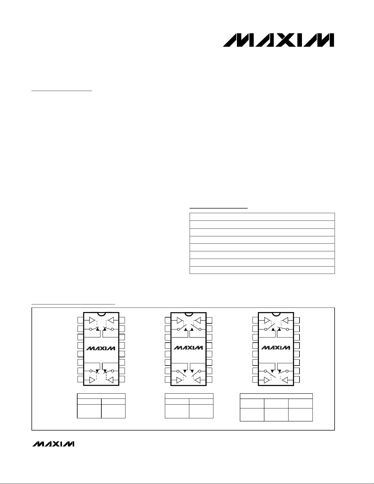
Ordering Information
SWITCHES SHOWN FOR LOGIC "0" INPUT
QSOP/SO/DIP
MAX4552
LOGIC SWITCH
0
1
OFF
ON
TOP VIEW
QSOP/SO/DIP
MAX4551
LOGIC SWITCH
0
1
ON
OFF
QSOP/SO/DIP
MAX4553
LOGIC
SWITCHES
1, 4
0
1
OFF
ON
SWITCHES
2, 3
ON
OFF
16
15
14
13
12
11
10
9
1
2
3
4
5
6
7
8
IN2
COM2
NC2
V+
V-
NO1
COM1
IN1
MAX4553
N.C.
NC3
COM3
IN3
IN4
COM4
NO4
GND
16
15
14
13
12
11
10
9
1
2
3
4
5
6
7
8
IN2
COM2
NC2
V+
V-
NC1
COM1
IN1
MAX4551
N.C.
NC3
COM3
IN3
IN4
COM4
NC4
GND
16
15
14
13
12
11
10
9
1
2
3
4
5
6
7
8
IN2
COM2
NO2
V+
V-
NO1
COM1
IN1
MAX4552
N.C.
NO3
COM3
IN3
IN4
COM4
NO4
GND
N.C. = NOT CONNECTED
Pin Configurations/Functional Diagrams/Truth Tables
Ordering Information continued at end of data sheet.
*
Contact factory for dice specifications.
PART
MAX4551CEE
MAX4551CSE
MAX4551CPE 0°C to +70°C
0°C to +70°C
0°C to +70°C
TEMP. RANGE PIN-PACKAGE
16 QSOP
16 Narrow SO
16 Plastic DIP
MAX4551C/D 0°C to +70°C Dice*
Rail-to-Rail is a registered trademark of Nippon Motorola, Ltd.
For free samples & the latest literature: http://www.maxim-ic.com, or phone 1-800-998-8800.
For small orders, phone 1-800-835-8769.
MAX4551EEE
MAX4551ESE -40°C to +85°C
-40°C to +85°C 16 QSOP
16 Narrow SO
MAX4551EPE -40°C to +85°C 16 Plastic DIP
MAX4551/MAX4552/MAX4553
±15kV ESD-Protected, Quad,
Low-Voltage, SPST Analog Switches
2 _______________________________________________________________________________________
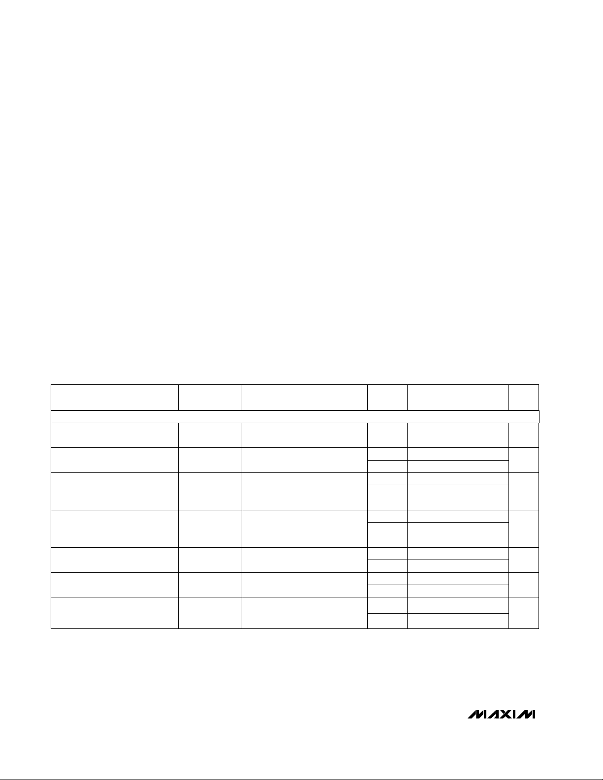
ABSOLUTE MAXIMUM RATINGS
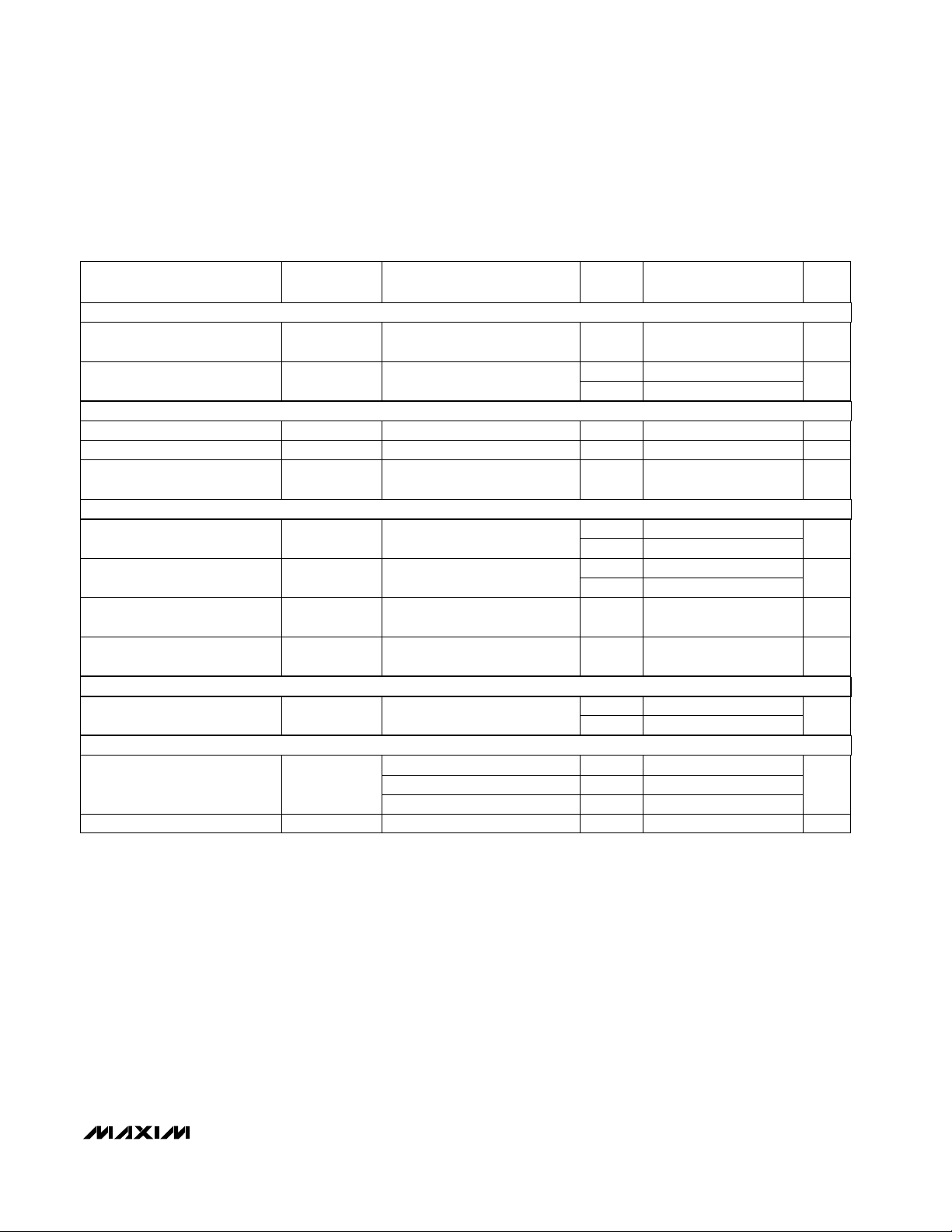
ELECTRICAL CHARACTERISTICS—Dual Supplies
(V+ = +5V, ±10%, V- = -5V, ±10%, TA= T
MIN
to T
MAX
, unless otherwise noted. Typical values are at TA= +25°C.)
Note 1: Signals on NC_, NO_, COM_, or IN_ exceeding V+ or V- are clamped by internal diodes. Limit forward-diode current to
maximum current rating.
Voltages Referenced to GND
V+.....................................................................-0.3V to +13.0V
V-.....................................................................-13.0V to +0.3V
V+ to V-............................................................-0.3V to +13.0V
All Other Pins (Note 1)..........................(V- - 0.3V) to (V+ + 0.3V)
Continuous Current into Any Terminal..............................±10mA
Peak Current into Any Terminal
(pulsed at 1ms,10% duty cycle)...................................±20mA
ESD per Method 3015.7 (IN_, COM_, V+, V-, GND) .......>2500V
IEC 1000-4-2 (NO_, NC_) ..................................................±15kV
Continuous Power Dissipation (T
A
= +70°C)
QSOP (derate 9.52mW/°C above +70°C)....................762mW
Narrow SO (derate 8.70mW/°C above +70°C) ............696mW
Plastic DIP (derate 10.53mW/°C above +70°C) ..........842mW
Operating Temperature Ranges
MAX455_C_E......................................................0°C to +70°C
MAX455_E_E ...................................................-40°C to +85°C
Storage Temperature Range.............................-65°C to +160°C
Lead Temperature (soldering, 10sec).............................+300°C
V+ = 5.5V, V- = -5.5V,
V
COM_
= ±4.5V
V+ = 5.5V, V- = -5.5V,
V
COM_
= ±4.5V, V
NO_
= 4.5V
V+ = 5V, V- = -5V, V
NO_
or V
NC_
= +3V, 0, -3V
V+ = 5.5V, V- = -5.5V,
V
COM_
= 4.5V, V
NO_
= ±4.5V
V+ = 5V, V- = -5V, V
NO_
or V
NC_
= ±3V, I
COM_
= 1mA
V+ = 5V, V- = -5V, V
NO_
or V
NC_
= ±3V, I
COM_
= 1mA
CONDITIONS
C, E
nAI
COM_(ON)
COM_ On-Leakage Current
(Note 6)
-20 20
-2 0.01 2
nAI
COM_(OFF)
COM_ Off-Leakage Current
(Note 6)
-10 10
nA
I
NO_(OFF)
,
I
NC_(OFF)
NO_, NC_ Off-Leakage Current
(Note 6)
-1 0.01 1
VV- V+
V
COM_
, V
NO_
,
V
NC_
Analog Signal Range
(Note 3)
Ω
10
R
FLAT(ON)
COM_ to NO_, COM_ to NC_
On-Resistance Flatness
(Note 5)
48
Ω
5
∆R
ON
COM_ to NO_, COM_ to NC_
On-Resistance Match Between
Channels (Note 4)
80 120
Ω
140
R
ON
COM_ to NO_, COM_ to NC_
On-Resistance
14
UNITS
MIN TYP MAX
(Note 2)
SYMBOLPARAMETER
C, E
+25°C
C, E
C, E
+25°C
+25°C
C, E
+25°C
C, E
+25°C
+25°C
T
A
±
±
-1 0.01 1
C, E -10 10
ANALOG SWITCH
Stresses beyond those listed under “Absolute Maximum Ratings” may cause permanent damage to the device. These are stress ratings only, and functional
operation of the device at these or any other conditions beyond those indicated in the operational sections of the specifications is not implied. Exposure to
absolute maximum rating conditions for extended periods may affect device reliability.
MAX4551/MAX4552/MAX4553
±15kV ESD-Protected, Quad,
Low-Voltage, SPST Analog Switches
_______________________________________________________________________________________ 3
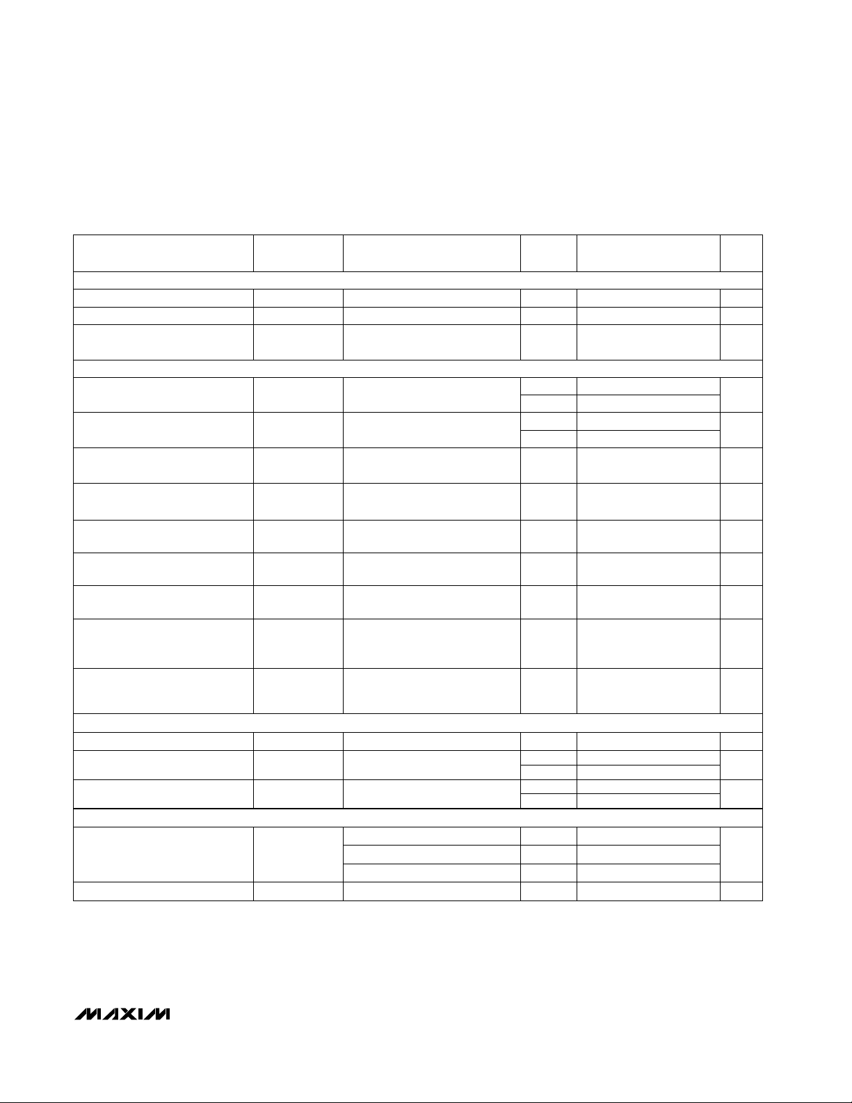
ELECTRICAL CHARACTERISTICS—Dual Supplies (continued)
(V+ = +5V, ±10%, V- = -5V, ±10%, TA= T
MIN
to T
MAX
, unless otherwise noted. Typical values are at TA= +25°C.)
Channel-to-Channel Crosstalk
(Note 8)
V
CT
C, EV
IN_
= 0.8V or 2.4V µA-1 0.03 1I
INH_
, I
INL_
IN_ Input Current Logic High
or Low
RL= 50Ω, CL= 15pF,
VN_= 1V
RMS
, f = 100kHz,
Figure 5
+25°C < -90
+25°C 70 110
dB
Turn-On Time
CONDITIONS
C, E
t
ON
C, E
V
COM_
= ±3V, V+ = 5V,
V- = -5V, Figure 1
V1.6 0.8V
IN_L
IN_ Input Logic Threshold Low
V2.4 1.6V
IN_H
IN_ Input Logic Threshold High
C, E 125
ns
+25°C 50 90
Turn-Off Time t
OFF
V
COM_
= ±3V, V+ = 5V,
V- = -5V, Figure 1
C, E 100
ns
Break-Before-Make Time Delay
(MAX4553 Only)
t
BBM
V
COM_
= ±3V, V+ = 5V,
V- = -5V, Figure 2
+25°C 520 ns
Charge Injection (Note 3) Q
CL= 1nF, V
NO_
= 0, RS= 0,
Figure 3
+25°C 25pC
NO_, NC_ Off-Capacitance C
N_(OFF)
V
NO_
= GND, f = 1MHz,
Figure 6
+25°C 3.5 pF
COM_ Off-Capacitance C
COM_(OFF)
V
COM_
= GND, f = 1MHz,
Figure 6
+25°C 3 pF
COM_ On-Capacitance C
COM_(ON)
V
COM_
= V
NO_
= GND,
f = 1MHz, Figure 7
+25°C 10 pF
Off-Isolation (Note 7)
UNITS
MIN TYP MAX
(Note 2)
SYMBOLPARAMETER
V
ISO
RL= 50Ω, CL= 15pF,
VN_= 1V
RMS
, f = 100kHz,
Figure 4
+25°C < -90 dB
T
A
Power-Supply Range V+, V- C, E ±2 ±6 V
+25°C -1 0.05 1
V+ Supply Current I+ V+ = 5.5V, all V
IN_
= 0 or V+
C, E -1 1
µA
+25°C -1 0.05 1
V- Supply Current I- V- = -5.5V
C, E -1 1
µA
+25°C ±8Contact Discharge IEC 1000-4-2
kV+25°C ±15
On NC_ and NO_ Pins
per IEC 801-2
Air Discharge IEC 1000-4-2
+25°C ±15Human Body Model
+25°C ±2.5All Pins MIL-STD-883C Method 3015 kV
SWITCH DYNAMIC CHARACTERISTICS
LOGIC INPUT
ESD PROTECTION
POWER SUPPLY
MAX4551/MAX4552/MAX4553
±15kV ESD-Protected, Quad,
Low-Voltage, SPST Analog Switches
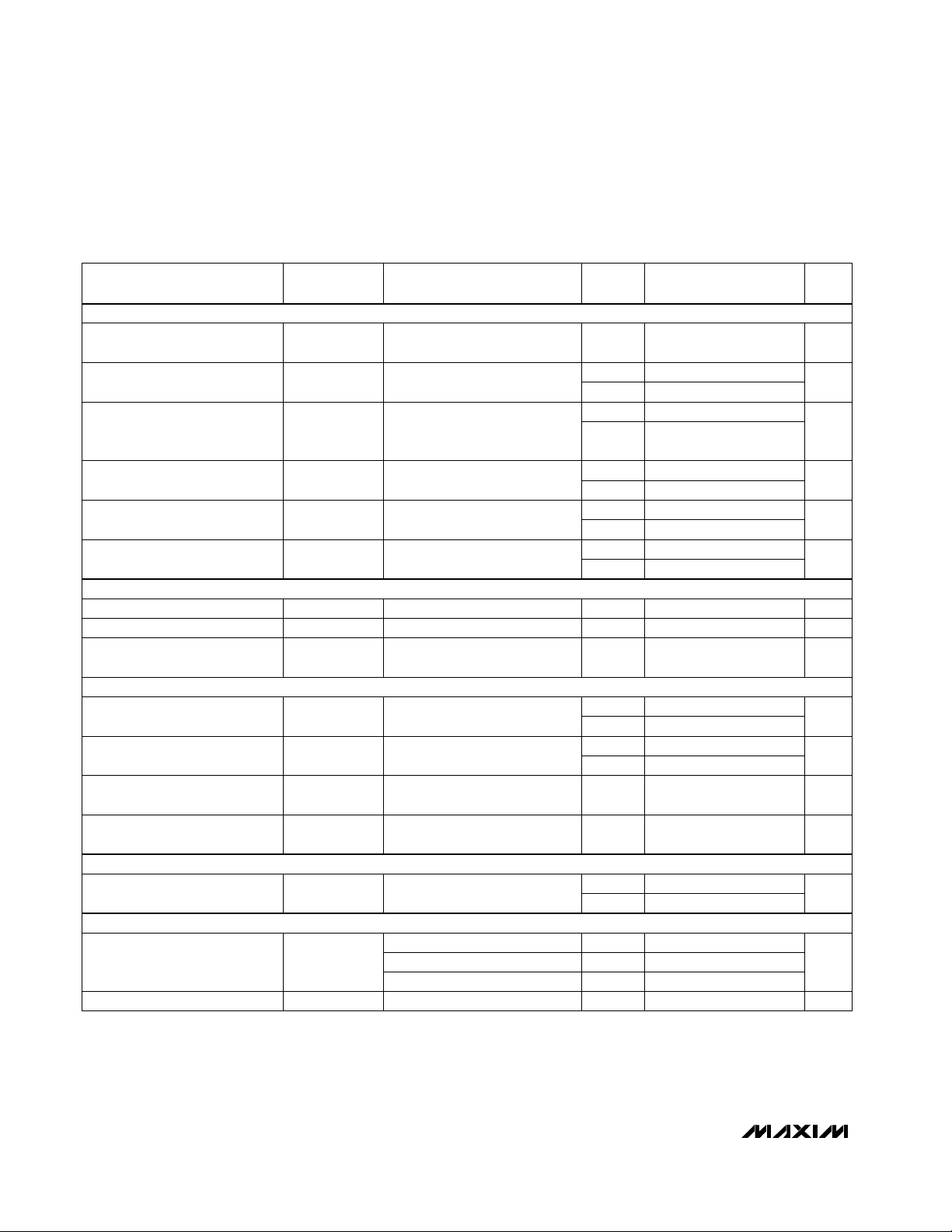
4 _______________________________________________________________________________________
+25°C
Charge Injection (Note 3)
(Note 3)
COM_ to NO_, COM_ to NC_
On-Resistance
Q
R
ON
V+ = 5V, V
COM_
= 3.5V,
I
COM_
= 1mA
C, E 180
Ω
CL= 1nF, V
NO_
= 0, RS= 0,
Figure 3
+25°C 15
+25°C 26
pC
COM_ to NO_, COM_ to NC_
On-Resistance Match Between
Channels (Note 4)
CONDITIONS
C, E
∆R
ON
V+ = 5V, V
COM_
= 3.5V,
I
COM_
= 1mA
115 160
V0V+
V
COM_
, V
NO_
,
V
NC_
Analog Signal Range
C, E 8
Ω
+25°C -1 0.01 1
C, E -10 10
NO_, NC_ Off-Leakage Current
(Notes 6, 9)
I
NO_(OFF)
,
I
NC_(OFF)
V+ = 5.5V; V
COM_
= 1V, 4.5V;
VN_= 4.5V, 1V
nA
+25°C -1 0.01 1
C, E -10 10
COM_ Off-Leakage Current
(Notes 6, 9)
I
COM_(OFF)
V+ = 5.5V; V
COM_
= 1V, 4.5V;
VN_= 4.5V, 1V
nA
+25°C -2 0.01 2
C, E, -20 20
COM_ On-Leakage Current
(Notes 6, 9)
I
COM_(ON)
V+ = 5.5V; V
COM_
= 4.5V, 1V nA
IN_ Input Logic Threshold High V
IN_H
C, E 2.4 1.6 V
IN_ Input Logic Threshold Low V
IN_L
C, E 1.6 0.8 V
UNITS
MIN TYP MAX
(Note 2)
SYMBOLPARAMETER
IN_ Input Current Logic High
or Low
I
INH_
, I
INL_
V
IN_
= 0.8V or 2.4V C, E -1 1 µA
T
A
+25°C 100 160
Turn-On Time t
ON
V
COM_
= 3V, V+ = 5V,
Figure 1
C, E 170
ns
+25°C 80 140
Turn-Off Time t
OFF
V
COM_
= 3V, V+ = 5V,
Figure 1
C, E 150
ns
+25°C 530
Break-Before-Make Time Delay
(MAX4553 Only)
t
BBM
V
COM_
= 3V, V+ = 5V,
Figure 2
ns
+25°C -1 0.05 1
V+ Supply Current I+ V+ = 5.5V, all V
IN_
= 0 or V+
C, E -1 1
µA
+25°C ±8
ELECTRICAL CHARACTERISTICS—Single +5V Supply
(V+ = +5V, ±10%, V- = -5V, ±10%, TA= T
MIN
to T
MAX
, unless otherwise noted. Typical values are at TA= +25°C.)
Contact Discharge IEC 1000-4-2
kV
On NC_ and NO_ Pins
per IEC 801-2
Human Body Model
+25°C ±15Air Discharge IEC 1000-4-2
+25°C ±15
kVAll Pins MIL-STD-883C Method 3015 +25°C ±2.5
ANALOG SWITCH
LOGIC INPUT
POWER SUPPLY
ESD PROTECTION
SWITCH DYNAMIC CHARACTERISTICS
MAX4551/MAX4552/MAX4553
±15kV ESD-Protected, Quad,
Low-Voltage, SPST Analog Switches
_______________________________________________________________________________________ 5
Note 2: The algebraic convention is used in this data sheet; the most negative value is shown in the minimum column.
Note 3: Guaranteed by design.
Note 4: ∆R
ON
= ∆R
ON(MAX)
- ∆R
ON(MIN)
.
Note 5: Resistance flatness is defined as the difference between the maximum and minimum on-resistance values, as measured
over the specified analog signal range.
Note 6: Leakage parameters are 100% tested at maximum rated temperature, and guaranteed by correlation at T
A
= +25°C.
Note 7: Off-isolation = 20log10 [ V
COM_
/ (V
NC_
or V
NO_
) ], V
COM_
= output, V
NC_
or V
NO_
= input to off switch.
Note 8: Between any two switches.
Note 9: Leakage testing for single-supply operation is guaranteed by testing with dual supplies.
ELECTRICAL CHARACTERISTICS—Single +3V Supply
(V+ = +2.7V to +3.6V, V- = 0, TA= T
MIN
to T
MAX
, unless otherwise noted. Typical values are at TA= +25°C.)
+25°C
Charge Injection
COM_ to NO_, COM_ to NC_
On-Resistance
Q
R
ON
V+ = 2.7V, V
COM_
= 1.0V,
I
COM_
= 0.1mA
C, E 500
Ω
IN_ Input Logic Threshold High V
IN_H
C, E 2.0 1.1 V
IN_ Input Logic Threshold Low
CONDITIONS
C, E
V
IN_L
CL= 1nF, V
NO_
= 0, RS= 0,
Figure 3
+25°C
200 400
15pC
V0V+
V
COM_
, V
NO_
,
V
NC_
Analog Signal Range
(Note 3)
C, E 1.1 0.5 V
IN_ Input Current Logic High
or Low
I
INH_
, I
INL_
V
IN_
= 0.8V or 2.4V C, E -1 0.03 1 µA
+25°C 190 350
Turn-On Time t
ON
V
COM_
= 1.5V, V+ = 2.7V,
Figure 1
C, E 400
ns
+25°C 160 250
Turn-Off Time t
OFF
V
COM_
= 1.5V, V+ = 2.7V,
Figure 1
C, E 300
ns
+25°C 10 50
Break-Before-Make Time Delay
(MAX4553 Only)
t
BBM
V
COM_
= 1.5V, V+ = 3.6V,
Figure 2
ns
+25°C -1 0.05 1
V+ Supply Current
UNITS
MIN TYP MAX
(Note 2)
SYMBOLPARAMETER
I+ V+ = 3.6V, all V
IN_
= 0 or V+
C, E -1 1
µA
T
A
SWITCH DYNAMIC CHARACTERISTICS (Note 4)
POWER SUPPLY
+25°C ±8Contact Discharge IEC 1000-4-2
+25°C ±15
+25°C ±15Human Body Model
On NC_ and NO_ Pins
per IEC 801-2
kV
Air Discharge IEC 1000-4-2
+25°C ±2.5MIL-STD-883C Method 3015All Pins kV
LOGIC INPUT
SWITCH DYNAMIC CHARACTERISTICS
POWER SUPPLY
ESD PROTECTION
ANALOG SWITCH

MAX4551/MAX4552/MAX4553
±15kV ESD-Protected, Quad,
Low-Voltage, SPST Analog Switches
6 _______________________________________________________________________________________
Typical Operating Characteristics
(V+ = +5V, V- = -5V, GND = 0, TA = +25°C, unless otherwise noted.)
60
100
80
70
90
110
120
130
-5 -3 -1-2-4 012345
ON-RESISTANCE
vs. V
COM
(DUAL SUPPLIES)
MAX4551-01
V
COM
(V)
R
ON
(Ω)
V+ = +2V
V- = -2V
V+ = +3V
V- = -3V
V+ = +4V
V- = -4V
V+ = +5V
V- = -5V
50
60
55
75
70
65
90
85
80
95
-6 -2-4 0246
ON-RESISTANCE
vs. V
COM
AND TEMPERATURE
(DUAL SUPPLIES)
MAX4551-02
V
COM
(V)
R
ON
(Ω)
TA = +85°C
TA = +25°C
TA = 0°C
TA = -40°C
V+ = +5V
V- = -5V
80
120
100
160
140
180
200
0231 456
ON-RESISTANCE
vs. V
COM
(SINGLE SUPPLY)
MAX4551-03
V
COM
(V)
RON (Ω)
V+ = +3.3V
V+ = +5V
V+ = +2.7V
V- = 0
60
90
70
80
100
110
120
130
0.0 1.51.00.5 2.52.0 3.53.0 4.0 4.5 5.0
ON-RESISTANCE
vs. V
COM
AND TEMPERATURE
(SINGLE SUPPLY)
MAX4551-04
V
COM
(V)
R
ON
(Ω)
TA = +25°C
TA = 0°C
TA = -40°C
TA = +85°C
V+ = +5V
V- = 0
0
40
20
60
120
160
140
100
80
200
180
-60 -40 -20 0 20 40 60 80 100
SCR HOLDING CURRENT
vs. TEMPERATURE
MAX4551-07
TEMPERATURE (°C)
HOLDING CURRENT (mA)
I
H-
I
H+
10n
0.1p
-55 -25 0 25 75
ON- AND OFF-LEAKAGE CURRENT
vs. TEMPERATURE
1p
1n
MAX4551-05
TEMPERATURE (°C)
LEAKAGE (A)
50 100 125
100p
10p
ON-LEAKAGE
OFF-LEAKAGE
-10
-6
-8
-2
-4
2
0
4
8
6
10
-5 -3 -2 -1-4 012 435
CHARGE INJECTION
vs. V
COM
MAX4551-06
V
COM
(V)
Q (pC)
V+ = +5V
V- = 0
V+ = +5V
V- = -5V
30
90
50
70
110
130
150
170
1.0 2.52.01.5 3.53.0 4.54.0 5.0 5.5 6.0
TURN-ON/TURN-OFF TIME
vs. SUPPLY VOLTAGE
MAX4551-08
SUPPLY VOLTAGE (V+, V-)
t
ON
, t
OFF
(ns)
t
ON
t
OFF
40
50
45
55
70
80
75
65
60
90
85
-60 -40 -20 0 20 40 60 80 100
TURN-ON/TURN-OFF TIME
vs. TEMPERATURE
MAX4551-09
TEMPERATURE (°C)
t
ON,
t
OFF
(ns)
t
OFF
t
ON

MAX4551/MAX4552/MAX4553
±15kV ESD-Protected, Quad,
Low-Voltage, SPST Analog Switches
_______________________________________________________________________________________ 7
Pin Description
10
0.0001
-60 -20-40 20 60 10080
POWER-SUPPLY CURRENT
vs. TEMPERATURE
0.001
0.01
0.1
1
MAX4551-10
TEMPERATURE (°C)
I+, I- (nA)
040
I-
I+
TOTAL HARMONIC DISTORTION
vs. FREQUENCY
MAX4551-11
FREQUENCY (Hz)
THD (%)
1
0.001
0.01
0.1
1 1k 10k 100k10 100 2M
V+ = +5V
V- = -5V
600Ω IN and OUT
100m 500m
-100
-90
-80
-70
-60
-40
-50
-30
-20
0
-10
100k 1m 10m
FREQUENCY RESPONSE
MAX4551-12
FREQUENCY (Hz)
LOSS (dB)
INSERTION LOSS
OFF-ISOLATION
ON-PHASE
50Ω IN/OUT
_____________________________Typical Operating Characteristics (continued)
(V+ = +5V, V- = -5V, GND = 0, TA= +25°C, unless otherwise noted.)
NAME FUNCTION
1, 16, 9, 8 IN1–IN4 Logic-Control Digital Inputs
2, 15, 10, 7 COM1–COM4 Analog Switch Common* Terminals
PIN
3, 14, 11, 6 NC1–NC4 Analog Switch Normally Closed Terminals
4 V-
Negative Analog Supply-Voltage Input. Connect to GND for singlesupply operation.
1, 16, 9, 8
2, 15, 10, 7
—
13 V+
Positive Analog and Digital Supply Voltage Input. Internally connected to substrate.
12 N.C. No Connection. Not internally connected.
—
4
13
12
5
1, 16, 9, 8
2, 15, 10, 7
NO1–NO4
—
4
13
12
5
MAX4551 MAX4552 MAX4553
5 GND
Ground. Connect to digital ground. (Analog signals have no ground
reference; they are limited to V+ and V-.)
Analog Switch Normally Open Terminals3, 14, 11, 6 —
— NO1, NO4 Analog Switch Normally Open Terminals— 3, 6
— NC2, NC3 Analog Switch Normally Closed Terminals— 14, 11
*NO_ (or NC_) and COM_ pins are identical and interchangeable. Either may be considered as an input or output; signals pass
equally well in either direction.

MAX4551/MAX4552/MAX4553
±15kV ESD-Protected, Quad,
Low-Voltage, SPST Analog Switches
8 _______________________________________________________________________________________
Applications Information
MAX4551/MAX4552/MAX4553
±15kV ESD Protection
The MAX4551/MAX4552/MAX4553 are ±15kV ESD-protected according to IEC 1000-4-2 at their NC/NO pins.
To accomplish this, bidirectional SCRs are included onchip between these pins and the GND pin. In normal
operation, these SCRs are off and have negligible
effect on the performance of the switches. When there
is an ESD strike at these pins, however, the voltages at
these pins go Beyond-the-Rails™ and cause the corresponding SCR(s) to turn on in a few nanoseconds and
bypass the surge safely to ground. This method is
superior to using diode clamps to the supplies because
unless the supplies are very carefully decoupled
through low ESR capacitors, the ESD current through
the diode clamp could cause a significant spike in the
supplies. This may damage or compromise the reliability of any other chip powered by those same supplies.
In the MAX4551/MAX4552/MAX4553, there are diodes
to the supplies in addition to the SCRs at the NC/NO
pins, but there is a resistance in series with these
diodes to limit the current into the supplies during an
ESD strike. The diodes are present to protect these
pins from overvoltages that are not as a result of ESD
strikes like those that may occur due to improper
power-supply sequencing.
Once the SCR turns on because of an ESD strike, it
continues to be on until the current through it falls
below its “holding current.” The holding current is typically 110mA in the positive direction (current flowing
into the NC/NO pin) and 95mA in the negative direction
at room temperature (see SCR Holding Current vs.
Temperature in the
Typical Operating Characteristics
).
The system should be designed such that any sources
connected to these pins are current limited to a value
below these to make sure the SCR turns off when the
ESD event gets over to resume normal operation. Also,
keep in mind that the holding current varies significantly with temperature. At +85°C, which represents the
worst case, the holding currents drop to 70mA and
65mA in the positive and negative directions respectively. Since these are typical numbers, to get guaranteed turn-off of the SCRs under all conditions, the
sources connected to these pins should be current limited to not more than half these values. When the SCR
is latched, the voltage across it is about ±3V, depending on the polarity of the pin current. The supply voltages do not affect the holding currents appreciably.
The sources connected to the COM side of the switches
do not need to be current limited since the switches are
made to turn off internally when the corresponding
SCR(s) get latched.
Even though most of the ESD current flows to GND
through the SCRs, a small portion of it goes into the
supplies. Therefore, it is a good idea to bypass the
supply pins with 100nF capacitors directly to the
ground plane.
ESD protection can be tested in various ways. Transmitter outputs and receiver inputs are characterized for
protection to the following:
• ±15kV using the Human Body Model
• ±8kV using the Contact Discharge method specified in IEC 1000-4-2 (formerly IEC 801-2)
• ±15kV using the Air-Gap Discharge method specified in IEC 1000-4-2 (formerly IEC 801-2).
ESD Test Conditions
Contact Maxim for a reliability report that documents
test setup, methodology, and results.
Human Body Model
Figure 8 shows the Human Body Model, and Figure 9
shows the current waveform it generates when discharged into a low impedance. This model consists of
a 100pF capacitor charged to the ESD voltage of interest, which is then discharged into the test device
through a 1.5kΩ resistor.
IEC 1000-4-2
The IEC 1000-4-2 standard covers ESD testing and
performance of finished equipment; it does not specifically refer to integrated circuits. The MAX4551/MAX4552/
MAX4553 enable the design of equipment that meets
Level 4 (the highest level) of IEC 1000-4-2, without
additional ESD protection components.
The major difference between tests done using the
Human Body Model and IEC 1000-4-2 is higher peak
current in IEC 1000-4-2. Because series resistance is
lower in the IEC 1000-4-2 ESD test model (Figure 10),
the ESD withstand voltage measured to this standard
is generally lower than that measured using the
Human Body Model. Figure 11 shows the current
waveform for the ±8kV IEC 1000-4-2 Level 4 ESD
Contact Discharge test.
The Air-Gap test involves approaching the device with
a charged probe. The Contact Discharge method
connects the probe to the device before the probe is
energized.
Beyond-the-Rails is a trademark of Maxim Integrated Products.

Power-Supply Considerations
Overview
The MAX4551/MAX4552/MAX4553 construction is typical of most CMOS analog switches. They have three
supply pins: V+, V-, and GND. V+ and V- are used to
drive the internal CMOS switches, and they set the limits of the analog voltage on any switch. Reverse ESDprotection diodes are internally connected between
each analog-signal pin and both V+ and V-. If any analog signal exceeds V+ or V-, one of these diodes conducts. During normal operation these reverse-biased
ESD diodes leak, forming the only current drawn from
V+ or V-.
Virtually all the analog leakage current is through the
ESD diodes. Although the ESD diodes on a given signal pin are identical and therefore fairly well balanced,
they are reverse biased differently. Each is biased by
either V+ or V- and the analog signal. This means their
leakages vary as the signal varies. The
difference
in the
two diode leakages from the signal path to the V+ and
V- pins constitutes the analog-signal-path leakage current. All analog leakage current flows to the supply terminals, not to the other switch terminal. This explains
how both sides of a given switch can show leakage
currents of the same or opposite polarity.
The analog signal paths consist of an N-channel and Pchannel MOSFET with their sources and drains paralleled, and their gates driven out of phase to V+ and Vby the logic-level translators.
V+ and GND power the internal logic and logic-level
translators, and set the input logic thresholds. The
logic-level translators convert the logic levels to
switched V+ and V- signals, to drive the gates of the
analog switches. This drive signal is the only connection between the logic supplies and the analog supplies. V+ and V- have ESD-protection diodes to GND.
The logic-level inputs and output have ESD protection
to V+ and to GND.
Increasing V- has no effect on the logic-level thresholds, but it does increase the drive to the P-channel
switches, reducing their on-resistance. V- also sets the
negative limit of the analog signal voltage.
The logic-level thresholds are CMOS/TTL compatible
when V+ = +5V. The threshold increases slightly as V+
is raised, and when V+ reaches +12V, the level threshold is about 3.1V. This is above the TTL output highlevel minimum of 2.8V, but still compatible with CMOS
outputs.
Bipolar Supplies
The MAX4551/MAX4552/MAX4553 operate with bipolar
supplies between ±2V and ±6V. The V+ and V- supplies need not be symmetrical, but their sum cannot
exceed the absolute maximum rating of 13.0V. Do not
connect the MAX4551/MAX4552/MAX4553 V+ to +3V,
and then connect the logic-level-input pins to TTL
logic-level signals. TTL logic-level outputs in excess
of the absolute maximum ratings can damage the
part and/or external circuits.
Caution: The absolute maximum V+ to V- differential
voltage is 13.0V. Typical ±6V or 12V supplies with
±10% tolerances can be as high as 13.2V. This voltage
can damage the MAX4551/MAX4552/MAX4553. Even
±5% tolerance supplies may have overshoot or noise
spikes that exceed 13.0V.
Single Supply
The MAX4551/MAX4552/MAX4553 operate from a
single supply between +2V and +12V when V- is connected to GND. All of the bipolar precautions must be
observed.
High-Frequency Performance
In 50Ω systems, signal response is reasonably flat up
to 50MHz (see
Typical Operating Characteristics
).
Above 20MHz, the on-response has several minor
peaks that are highly layout-dependent. The problem
with high-frequency operation is not turning the switch
on, but turning it off. The off-state switch acts like a
capacitor and passes higher frequencies with less
attenuation. At 10MHz, off-isolation is about -52dB in
50Ω systems, becoming worse (approximately 20dB
per decade) as frequency increases. Higher circuit
impedances also make off-isolation worse. Adjacent
channel attenuation is about 3dB above that of a bare
IC socket, and is due entirely to capacitive coupling.
MAX4551/MAX4552/MAX4553
±15kV ESD-Protected, Quad,
Low-Voltage, SPST Analog Switches
_______________________________________________________________________________________ 9

MAX4551/MAX4552/MAX4553
±15kV ESD-Protected, Quad,
Low-Voltage, SPST Analog Switches
10 ______________________________________________________________________________________
V
GEN
GND
NC or
NO
C
L
V
OUT
-5V
V-
V+
V
OUT
IN
OFF
ON
OFF
∆V
OUT
Q = (∆V
OUT
)(CL)
COM
IN DEPENDS ON SWITCH CONFIGURATION;
INPUT POLARITY DETERMINED BY SENSE OF SWITCH.
OFF
ON
OFF
IN
V
IN
= +3V
+5V
R
GEN
IN
MAX4551
MAX4552
MAX4553
Figure 3. Charge Injection
tr < 20ns
tf < 20ns
50%
0V
LOGIC
INPUT
V-
-5V
R
L
300Ω
NO
or NC
GND
C
L
INCLUDES FIXTURE AND STRAY CAPACITANCE.
V
OUT
= V
COM (
R
L
)
RL + R
ON
SWITCH
INPUT
IN, EN
+3V
t
OFF
0V
COM
SWITCH
OUTPUT
0.9 · V
0UT
0.9 · V
OUT
t
ON
V
OUT
SWITCH
OUTPUT
LOGIC
INPUT
LOGIC INPUT WAVEFORMS INVERTED FOR EN AND SWITCHES
THAT HAVE THE OPPOSITE LOGIC SENSE.
C
L
35pF
+5V
V+
V
OUT
V
COM
0V
MAX4551
MAX4552
MAX4553
Figure 1. Switching Time
Figure 2. Break-Before-Make Interval (MAX4553 only)
Test Circuits/Timing Diagrams
MAX4553
COM1
COM2
COM1
COM2
IN1, 2
V
V
LOGIC
INPUT
C
GND
INCLUDES FIXTURE AND STRAY CAPACITANCE.
L
+5V
-5V
OUT1
OUT2
+3V
0V
0V
)
)
0V
LOGIC
V+
NO
NC
V-
V
OUT2
R
C
L2
L2
RL = 300Ω
= 35pF
C
L
V
OUT1
R
C
L1
L1
INPUT
SWITCH
OUTPUT 1
(V
SWITCH
OUTPUT 2
(V
50%
t
D
0.9 · V
0UT1
0.9 · V
OUT2
t
D

MAX4551/MAX4552/MAX4553
±15kV ESD-Protected, Quad,
Low-Voltage, SPST Analog Switches
______________________________________________________________________________________ 11
Figure 5. Crosstalk
IN
0 or
2.4V
SIGNAL
GENERATOR 0dBm
+5V
10nF
ANALYZER
NC
or NO
R
L
GND
COM
10nF
V-
V-
V+
MAX4551
MAX4552
MAX4553
Figure 4. Off-Isolation
Test Circuits/Timing Diagrams (continued)
CAPACITANCE
METER
NC
or NO
COM
GND
10nF
V-
V-
IN
0 or
2.4V
10nF
+5V
f = 1MHz
V+
MAX4551
MAX4552
MAX4553
Figure 7. Channel On-Capacitance
CAPACITANCE
METER
NC
or NO
COM
GND
10nF
V-
V-
IN
0 or
2.4V
10nF
+5V
f = 1MHz
V+
MAX4551
MAX4552
MAX4553
Figure 6. Channel Off-Capacitance
V-
V-
N01
IN2
COM2
MAX4551
MAX4552
MAX4553
50Ω
0 or 2.4V
NC
10nF
SIGNAL
GENERATOR 0dBm
0V or 2.4V
ANALYZER
+5V
10nF
V+
COM1
IN1
N02
R
L
GND

MAX4551/MAX4552/MAX4553
±15kV ESD-Protected, Quad,
Low-Voltage, SPST Analog Switches
12 ______________________________________________________________________________________
CHARGE-CURRENT
LIMIT RESISTOR
DISCHARGE
RESISTANCE
STORAGE
CAPACITOR
C
s
100pF
R
C
1M
R
D
1500Ω
HIGH-
VOLTAGE
DC
SOURCE
DEVICE
UNDER
TEST
Figure 8. Human Body ESD Test Model
Figure 9. Human Body Model Current Waveform
CHARGE-CURRENT
LIMIT RESISTOR
DISCHARGE
RESISTANCE
STORAGE
CAPACITOR
C
s
150pF
R
C
50M to 100M
R
D
330Ω
HIGH-
VOLTAGE
DC
SOURCE
DEVICE
UNDER
TEST
Figure 10. IEC 1000-4-2 ESD Test Model
tr = 0.7ns to 1ns
30ns
60ns
t
100%
90%
10%
I
PEAK
I
Figure 11. IEC 1000-4-2 ESD Generator Current Waveform
AMPERES
IP 100%
90%
36.8%
10%
PEAK-TO-PEAK RINGING
I
r
(NOT DRAWN TO SCALE)
0
0
t
RL
TIME
t
DL
CURRENT WAVEFORM

MAX4551/MAX4552/MAX4553
±15kV ESD-Protected, Quad,
Low-Voltage, SPST Analog Switches
______________________________________________________________________________________ 13
Chip Topographies
COM3
IN3
IN4
COM4
NC2
NC3
V+
0.080"
(2.03mm)
0.061"
(1.55mm)
NC1
V-
NC4
GND
COM2
IN2
IN1
COM1
MAX4551
COM3
IN3
IN4
COM4
NO2
NO3
V+
0.080"
(2.03mm)
0.061"
(1.55mm)
NO1
V-
N04
GND
COM2
IN2
IN1
COM1
MAX4552
COM3
IN3
IN4
COM4
NC2
NC3
V+
0.080"
(2.03mm)
0.061"
(1.55mm)
NO1
V-
N04
GND
COM2
IN2
IN1
COM1
MAX4553
TRANSISTOR COUNT: 126
SUBSTRATE CONNECTED
TO GND

MAX4551/MAX4552/MAX4553
±15kV ESD-Protected, Quad,
Low-Voltage, SPST Analog Switches
14 ______________________________________________________________________________________
*
Contact factory for dice specifications.
Ordering Information (continued)
Package Information
QSOP.EPS
PART
MAX4552CEE
MAX4552CSE
MAX4552CPE 0°C to +70°C
0°C to +70°C
0°C to +70°C
TEMP. RANGE PIN-PACKAGE
16 QSOP
16 Narrow SO
16 Plastic DIP
MAX4552C/D 0°C to +70°C Dice*
MAX4552EEE
MAX4552ESE -40°C to +85°C
-40°C to +85°C 16 QSOP
16 Narrow SO
MAX4552EPE -40°C to +85°C 16 Plastic DIP
MAX4553CEE
MAX4553CSE
MAX4553CPE 0°C to +70°C
0°C to +70°C
0°C to +70°C 16 QSOP
16 Narrow SO
16 Plastic DIP
MAX4553C/D 0°C to +70°C Dice*
MAX4553EEE
MAX4553ESE -40°C to +85°C
-40°C to +85°C 16 QSOP
16 Narrow SO
MAX4553EPE -40°C to +85°C 16 Plastic DIP

MAX4551/MAX4552/MAX4553
±15kV ESD-Protected, Quad,
Low-Voltage, SPST Analog Switches
______________________________________________________________________________________ 15
Package Information (continued)
SOICN.EPS

MAX4551/MAX4552/MAX4553
±15kV ESD-Protected, Quad,
Low-Voltage, SPST Analog Switches
Maxim cannot assume responsibility for use of any circuitry other than circuitry entirely embodied in a Maxim product. No circuit patent licenses are
implied. Maxim reserves the right to change the circuitry and specifications without notice at any time.
16
____________________Maxim Integrated Products, 120 San Gabriel Drive, Sunnyvale, CA 94086 408-737-7600
© 1998 Maxim Integrated Products Printed USA is a registered trademark of Maxim Integrated Products.
Package Information (continued)
PDIPN.EPS
 Loading...