

_______________General Description
The MAX4545/MAX4546/MAX4547 are low-voltage
T-switches designed for switching RF and video signals
from DC to 300MHz in 50Ω and 75Ω systems. The
MAX4545 contains four normally open single-pole/singlethrow (SPST) switches. The MAX4546 contains two dual
SPST switches (one normally open, one normally closed.)
The MAX4547 contains two single-pole/double-throw
(SPDT) switches.
Each switch is constructed in a “T” configuration, ensuring
excellent high-frequency off isolation and crosstalk of
-80dB at 10MHz. They can handle Rail-to-Rail
®
analog signals in either direction. On-resistance (20Ω max) is
matched between switches to 1Ω max and is flat (0.5Ω
max) over the specified signal range, using ±5V supplies.
The off leakage current is less than 5nA at +25°C and
50nA at +85°C.
These CMOS switches can operate with dual power supplies ranging from ±2.7V to ±6V or a single supply
between +2.7V and +12V. All digital inputs have 0.8V/2.4V
logic thresholds, ensuring both TTL- and CMOS-logic compatibility when using ±5V or a single +5V supply.
________________________Applications
RF Switching
Video Signal Routing
High-Speed Data Acquisition
Test Equipment
ATE Equipment
Networking
____________________________Features
♦ Low 50Ω Insertion Loss: -1dB at 100MHz
♦ High 50Ω Off Isolation: -80dB at 10MHz
♦ Low 50Ω Crosstalk: -80dB at 10MHz
♦ DC to 300MHz -3dB Signal Bandwidth
♦ 20Ω Signal Paths with ±5V Supplies
♦ 1Ω Signal-Path Matching with ±5V Supplies
♦ 0.5Ω Signal-Path Flatness with ±5V Supplies
♦ ±2.7V to ±6V Dual Supplies
+2.7V to +12V Single Supply
♦ Low Power Consumption: <1µW
♦ Rail-to-Rail Bidirectional Signal Handling
♦ Pin Compatible with Industry-Standard DG540,
DG542, DG643
♦ >2kV ESD Protection per Method 3015.7
♦ TTL/CMOS-Compatible Inputs
with Single +5V or ±5V
MAX4545/MAX4546/MAX4547
Quad/Dual, Low-Voltage,
Bidirectional RF/Video Switches
________________________________________________________________
Maxim Integrated Products
1
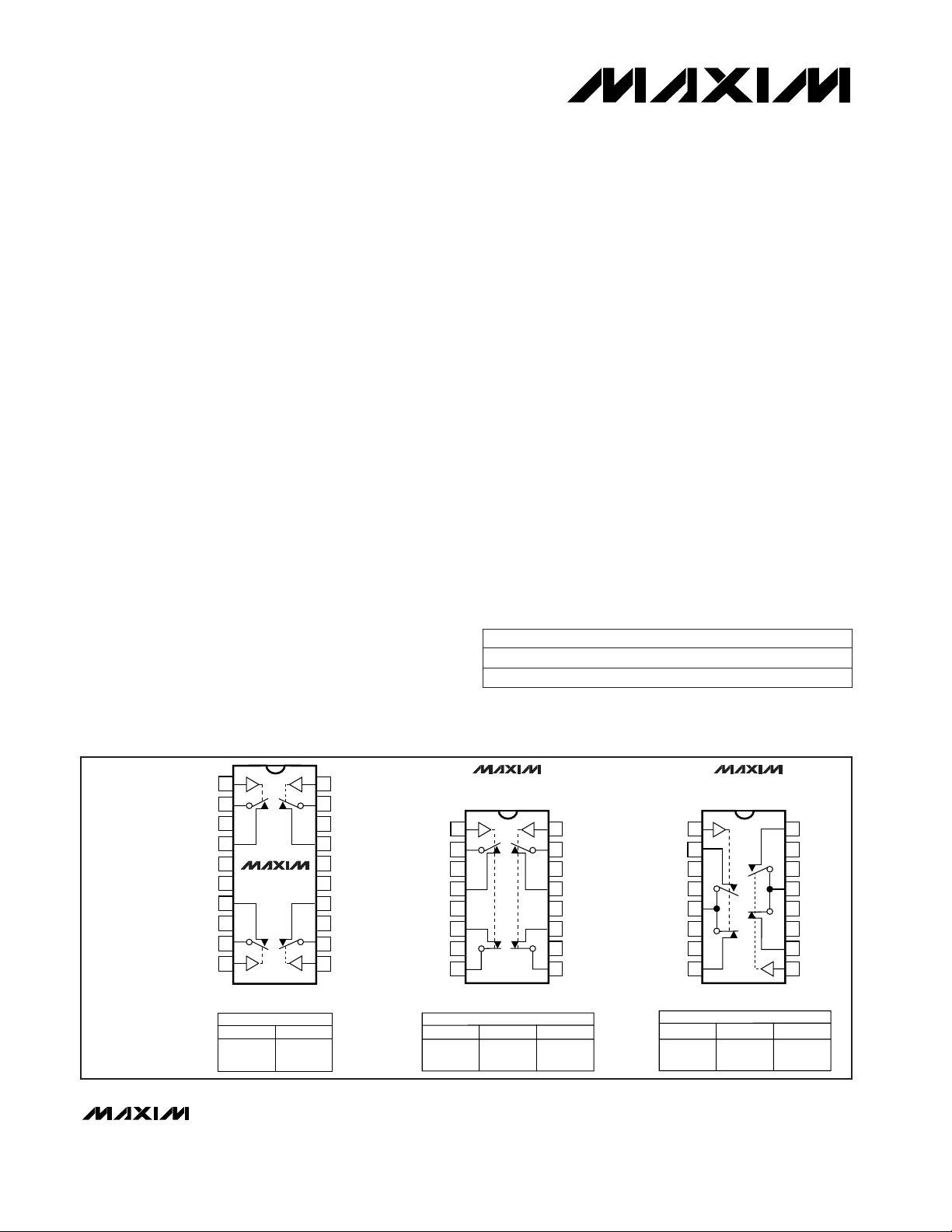
TOP VIEW
16
15
14
13
12
11
10
9
1
2
3
4
5
6
7
8
MAX4546
DIP/SO/QSOP
IN2
COM2
GND2
NO2
V+
NC3
GND3
COM3
N01
GND1
COM1
IN1
COM4
GND4
NC4
V-
20
19
18
17
16
15
14
13
1
2
3
4
5
6
7
8
IN2
COM2
GND2
NO2N01
GND1
COM1
IN1
V+
GND6
N03
GND3GND4
N04
GND5
V-
12
11
9
10
COM3
IN3IN4
COM4
MAX4545
DIP/SO/SSOP
16
15
14
13
12
11
10
9
1
2
3
4
5
6
7
8
MAX4547
DIP/SO/QSOP
N02
V+
GND2
COM2
GND3
VNC2
IN2
GND1
V-
N01
IN1
NC1
V+
GND4
COM1
MAX4545
SWITCHES SHOWN
FOR LOGIC “0” INPUT
LOGIC SWITCH
0
1
OFF
ON
MAX4547
LOGIC NO-COM
0
1
OFF
ON
NC-COM
ON
OFF
MAX4546
LOGIC 1, 2
0
1
OFF
ON
3, 4
ON
OFF
_____________________Pin Configurations/Functional Diagrams/Truth Tables
19-1232; Rev 0; 6/97
______________Ordering Information
Ordering Information continued at end of data sheet.
For free samples & the latest literature: http://www.maxim-ic.com, or phone 1-800-998-8800
Rail-to-Rail is a registered trademark of Nippon Motorola Ltd.
PART
MAX4545CPP
MAX4545CWP 0°C to +70°C
0°C to +70°C
TEMP. RANGE PIN-PACKAGE
20 Plastic DIP
20 Wide SO
MAX4545/MAX4546/MAX4547
Quad/Dual, Low-Voltage,
Bidirectional RF/Video Switches
2 _______________________________________________________________________________________
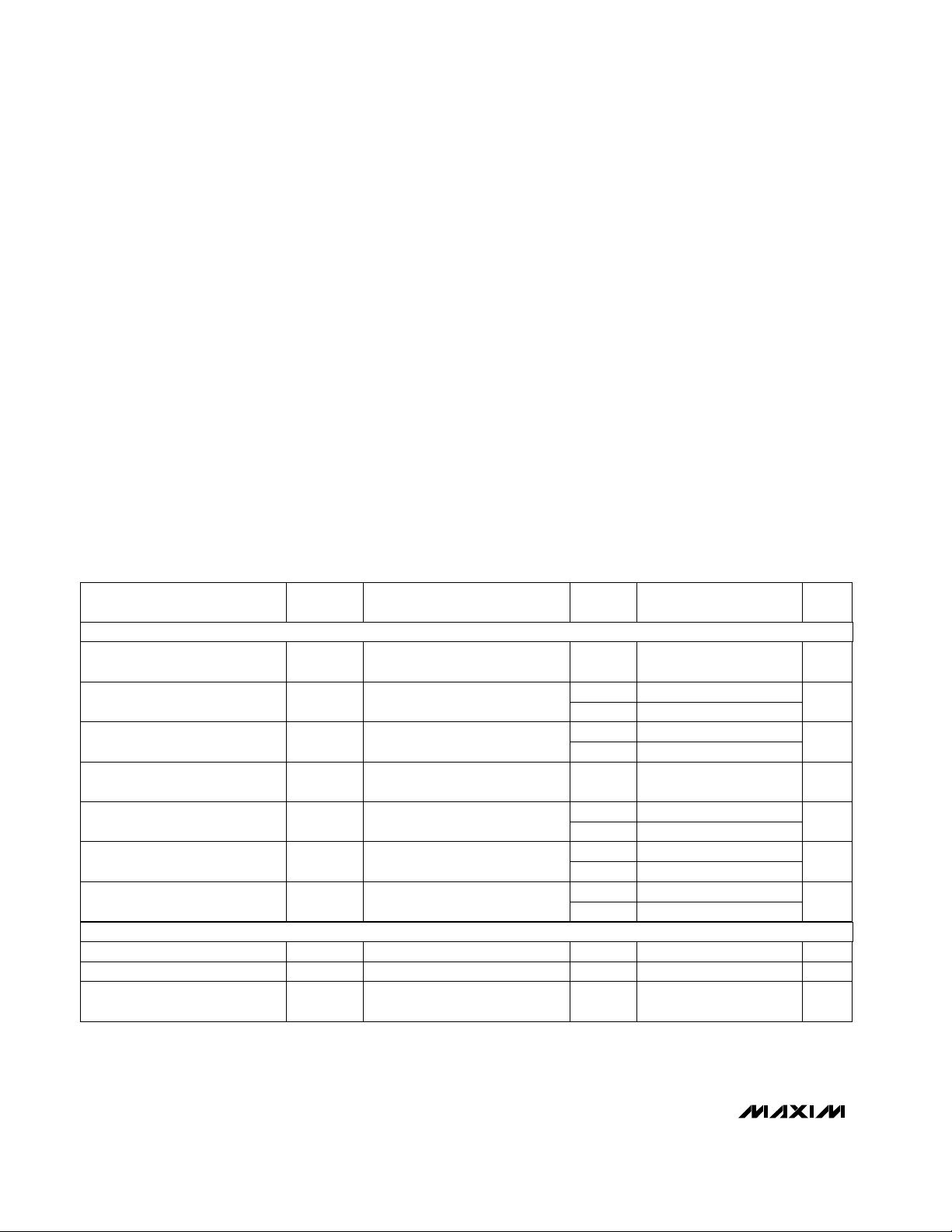
ABSOLUTE MAXIMUM RATINGS
ELECTRICAL CHARACTERISTICS—Dual Supplies
(V+ = +4.5V to +5.5V, V- = -4.5V to -5.5V, V
INL
= 0.8V, V
INH
= 2.4V, V
GND_
= 0V, TA= T
MIN
to T
MAX
, unless otherwise noted. Typical
values are at T
A
= +25°C.)
Stresses beyond those listed under “Absolute Maximum Ratings” may cause permanent damage to the device. These are stress ratings only, and functional
operation of the device at these or any other conditions beyond those indicated in the operational sections of the specifications is not implied. Exposure to
absolute maximum rating conditions for extended periods may affect device reliability.
(Voltages Referenced to GND)
V+...........................................................................-0.3V, +13.0V
V-............................................................................-13.0V, +0.3V
V+ to V-...................................................................-0.3V, +13.0V
All Other Pins (Note 1)..........................(V- - 0.3V) to (V+ + 0.3V)
Continuous Current into Any Terminal..............................±25mA
Peak Current into Any Terminal
(pulsed at 1ms, 10% duty cycle)..................................±50mA
ESD per Method 3015.7 ..................................................>2000V
Continuous Power Dissipation (T
A
= +70°C) (Note 2)
16-Pin Plastic DIP
(derate 10.53mW/°C above +70°C)..........................842mW
16-Pin Narrow SO
(derate 8.70mW/°C above +70°C)............................696mW
16-Pin QSOP (derate 8.3mW/°C above +70°C).......... 667mW
20-Pin Plastic DIP (derate 8.0mW/°C above +70°C) ...640mW
20-Pin Wide SO (derate 10.00mW/°C above +70°C) .. 800mW
20-Pin SSOP (derate 8.0mW/°C above +70°C) .......... 640mW
Operating Temperature Ranges
MAX454_C_ E.....................................................0°C to +70°C
MAX454_E_ E ..................................................-40°C to +85°C
Storage Temperature Range.............................-65°C to +150°C
Lead Temperature (soldering, 10sec).............................+300°C
Note 1: Voltages on all other pins exceeding V+ or V- are clamped by internal diodes. Limit forward diode current to maximum cur-
rent rating.
V+ = 4.5V, V- = -4.5V,
V
COM_
= ±2V, I
COM_
= 10mA
(Note 3)
V+ = 5.5V, V- = -5.5V,
V
COM_
= ±4.5V, VN_= 4.5V
V+ = 4.5V, V- = -4.5V,
V
COM_
= ±2V, I
COM_
= 10mA
V+ = 5V; V- = -5V; V
COM_
= 1V,
0V, -1V; I
COM
= 10mA
V+ = 5.5V, V- = -5.5V,
V
COM_
= ±4.5V, VN_= 4.5V
V+ = 5.5V, V- = -5.5V,
V
COM_
= ±4.5V, VN_= 4.5V
V
IN_
= 0.8V or 2.4V
CONDITIONS
µA-1 0.03 1I
INH_
, I
INL_
IN_ Input Current Logic High or
Low
Ω
14 20
R
ON
Signal-Path On-Resistance
VV- V+
V
COM_
,
V
NO_,VNC_
Analog Signal Range
V0.8 1.5V
IN_L
IN_ Input Logic Threshold Low
V1.5 2.4V
IN_H
IN_ Input Logic Threshold High
nA
-10 0.04 10
I
COM_(ON)
COM_ On Leakage Current
(Note 6)
Ω
0.5 1
∆R
ON
Signal-Path On-Resistance Match
Between Channels (Note 4)
Ω0.3 0.5R
FLAT(ON)
Signal-Path On-Resistance
Flatness (Note 5)
nA
-5 0.02 5
I
NO_(OFF)
,
I
NC_(OFF)
NO_, NC_ Off Leakage Current
(Note 6)
nA
-5 0.02 5
I
COM_(OFF)
COM_ Off Leakage Current
(Note 6)
UNITS
MIN TYP MAX
(Note 2)
SYMBOLPARAMETER
+25°C
C, E
C, E
C, E
+25°C
+25°C
+25°C
+25°C
+25°C
C, E
T
A
C, E
C, E
C, E -50 50
-50 50
-100 100
C, E
C, E 1.25
18 25
ANALOG SWITCH
LOGIC INPUT
±
±
±
MAX4545/MAX4546/MAX4547
Quad/Dual, Low-Voltage,
Bidirectional RF/Video Switches
_______________________________________________________________________________________ 3
VIN= 5Vp-p, f < 20kHz,
600Ω in and out
Figure 7, RL= 50Ω
V
NO_
= GND, f = 1MHz, Figure 8
CL= 1.0nF, V
NO_
= 0V, RS = 0Ω,
Figure 6
V
COM_
= ±3V, V+ = 5V, V- = -5V,
Figure 5 (Note 3)
V
COM_
= ±3V, V+ = 5V, V- = -5V,
Figure 4
V
COM_
= ±3V, V+ = 5V, V- = -5V,
Figure 4
CONDITIONS
%0.004THD+NDistortion
MHz300BW-3dB Bandwidth
-80
11.5
COM_ Off Capacitance
pF6C
N_(OFF)
NO_, NC_ Off Capacitance
pC60 150Q
Charge Injection
(Note 3)
ns15 40t
BBM
Break-Before-Make Time Delay
(MAX4546/MAX4547 only)
ns
35 100
t
OFF
Turn-Off Time
ns
90 150
t
ON
Turn-On Time
UNITS
MIN TYP MAX
(Note 2)
SYMBOLPARAMETER
V- = -5.5V
V+ = 5.5V, all V
IN_
= 0V or V+
µA
-1 0.05 1
I-V - Supply Current
µA
-1 0.05 1
I+V+ Supply Current
V-6 +6V+, V-Power-Supply Range
+25°C
+25°C
+25°C
+25°C
+25°C
+25°C
+25°C
T
A
+25°C
+25°C
C, E
6
V
COM_
= 0V,
f = 1MHz,
Figure 8
pFC
COM_(OFF)
+25°C
11.5
V
COM_
= V
NO_
= 0V,
f = 1MHz, Figure 8
pF
17
C
COM_(ON)
COM_ On Capacitance +25°C
-80
RL= 50Ω,
V
COM_
= 1V
RMS
,
f = 10MHz, Figure 7
dB
-82
V
ISO
Off Isolation (Note 7) +25°C
MAX4545
MAX4545
MAX4546
MAX4547
MAX4545
MAX4546
MAX4547
C, E -10 10
C, E -10 10
C, E 120
C, E 200
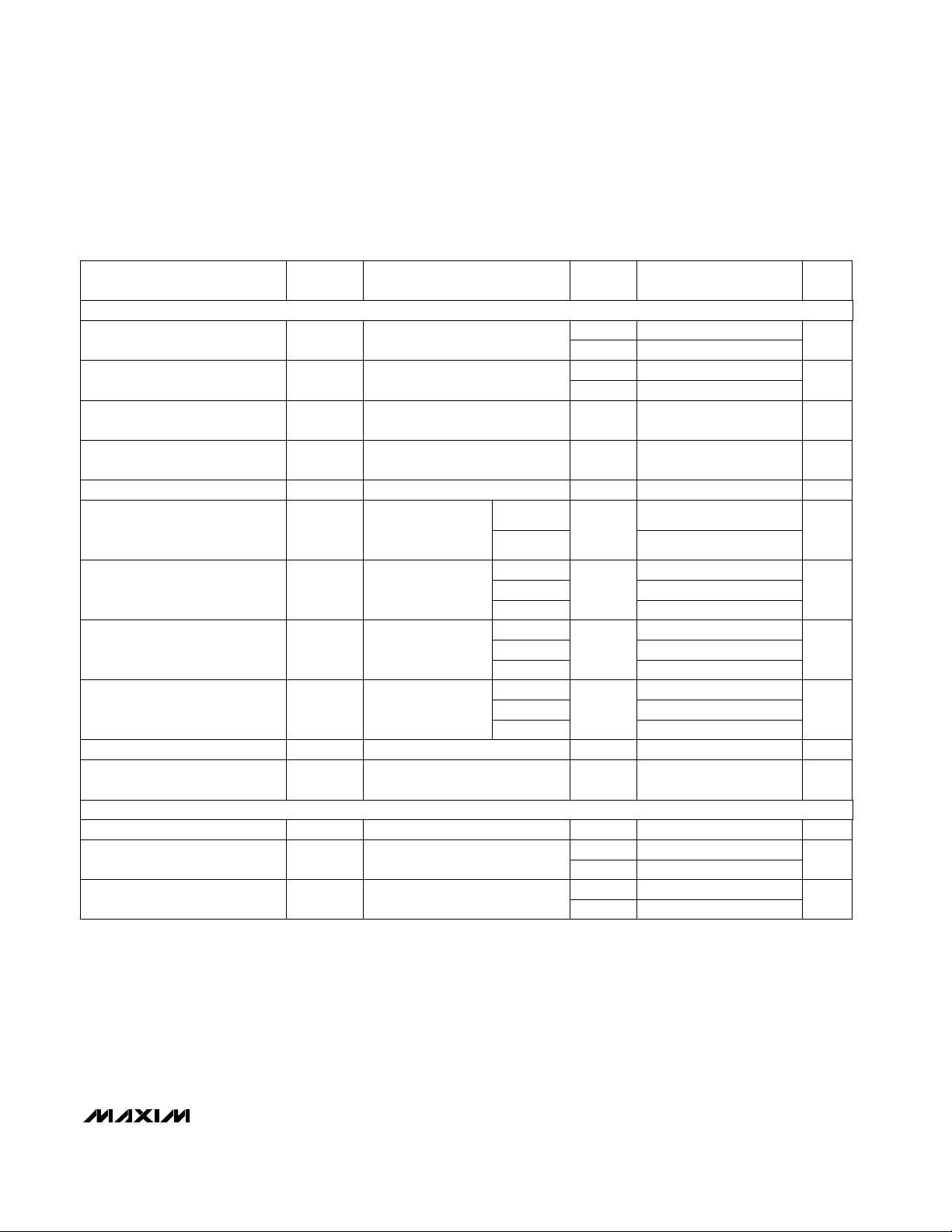
ELECTRICAL CHARACTERISTICS—Dual Supplies (continued)
(V+ = +4.5V to +5.5V, V- = -4.5V to -5.5V, V
INL
= 0.8V, V
INH
= 2.4V, V
GND_
= 0V, TA= T
MIN
to T
MAX
, unless otherwise noted. Typical
values are at T
A
= +25°C.)
MAX4546 6
-88MAX4545
MAX4546
MAX4547
-80
RL= 50Ω, V
COM_
=
1V
RMS
, f = 10MHz,
Figure 7
dB
-84
V
CT
Channel-to-Channel Crosstalk
(Note 8)
+25°C
SWITCH DYNAMIC CHARACTERISTICS
POWER SUPPLY
MAX4545/MAX4546/MAX4547
Quad/Dual, Low-Voltage,
Bidirectional RF/Video Switches
4 _______________________________________________________________________________________
CL= 1.0nF, VNO= 2.5V,
RS= 0Ω, Figure 6
V
COM_
= 3V, V+ = 5V,
Figure 5 (Note 3)
V+ = 4.5V, V
COM_
= 3.5V,
I
COM_
= 1mA
V
COM_
= 3V, V+ = 5V,
Figure 4
(Note 3)
V
COM_
= 3V, V+ = 5V,
Figure 4
V
IN_
= 0.8V or 2.4V
V+ = 5.5V; V
COM_
= 1V, 4.5V
V+ = 5.5V, V
COM_
= 1V,
VN_= 4.5V
V+ = 4.5V, V
COM_
= 3.5V,
I
COM_
= 1mA
V+ = 5.5V, V
COM_
= 1V,
VN_= 4.5V
CONDITIONS
pC25QCharge Injection
ns20 70t
BBM
Break-Before-Make Time Delay
(MAX4546/MAX4547 only)
ns
150
40 100
t
OFF
Turn-Off Time
ns
350
130 250
t
ON
Turn-On Time
µA-1 0.03 1I
INH_
, I
INL_
IN_ Input Current Logic High or
Low
V0.8 1.5V
IN_L
IN_ Input Logic Threshold Low
V1.5 2.4V
IN_H
IN_ Input Logic Threshold High
nA
-100 100
26 40
R
ON
Signal-Path On-Resistance
V0 V+
V
COM_
,
V
NO_
, V
NC_
Analog Signal Range
-10 0.04 10
I
COM_(ON)
COM_ On Leakage Current
(Note 9)
nA
-50 50
-5 0.02 5
I
COM_(OFF)
COM_ Off Leakage Current
(Note 9)
nA
-50 50
Ω
60
2
∆R
ON
Signal-Path On-Resistance
Match
Ω
4
-5 0.02 5
I
NO_(OFF)
,
I
NC_(OFF)
NO_, NC_ Off Leakage Current
(Note 9)
UNITS
MIN TYP MAX
(Note 2)
SYMBOLPARAMETER
+25°C
+25°C
+25°C
C, E
+25°C
+25°C
C, E
+25°C
C, E
+25°C
C, E
C, E
C, E
+25°C
C, E
C, E
+25°C
C, E
+25°C
C, E
T
A
ELECTRICAL CHARACTERISTICS—Single +5V Supply
(V+ = +4.5V to +5.5V, V- = 0V, V
INL
= 0.8V, V
INH
= 2.4V, V
GND_
= 0V, TA= T
MIN
to T
MAX
, unless otherwise noted. Typical values are
at T
A
= +25°C.)
V+ = 5.5V, all V
IN_
= 0V or V+
-1 0.05 1
I+V+ Supply Current µA
-10 10
+25°C
C, E
RL= 50Ω, V
COM_
= 1V
RMS
,
f = 10MHz, Figure 7
dB-75V
ISO
Off-Isolation
(Note 7)
+25°C
RL= 50Ω, V
COM_
= 1V
RMS
,
f = 10MHz, Figure 7
dB-70V
CT
Channel-to-Channel Crosstalk
(Note 8)
+25°C
ANALOG SWITCH
LOGIC INPUT
SWITCH DYNAMIC CHARACTERISTICS
POWER SUPPLY
V+ Supply Current
MAX4545/MAX4546/MAX4547
Quad/Dual, Low-Voltage,
Bidirectional RF/Video Switches
_______________________________________________________________________________________ 5
ELECTRICAL CHARACTERISTICS—Single +3V Supply
(V+ = +2.7V to +3.6V, V- = 0V, V
INL
= 0.8V, V
INH
= 2.4V, V
GND_
= 0V, TA= T
MIN
to T
MAX
, unless otherwise noted. Typical values are
at T
A
= +25°C.)
V+ = 2.7V, V
COM_
= 1V,
I
COM_
= 1mA
(Note 3)
V+ = 3.6V, all V
IN_
= 0V or V+
V
COM_
= 1.5V, V+ = 2.7V,
Figure 4 (Note 3)
V
COM_
= 1.5V, V+ = 2.7V,
Figure 5 (Note 3)
V
IN_
= 0.8V or 2.4V (Note 3)
(Note 3)
(Note 3)
V
COM_
= 1.5V, V+ = 2.7V,
Figure 4 (Note 3)
CONDITIONS
µA
-1 0.05 1
I+V+ Supply Current
ns15 100t
BBM
Break-Before-Make Time Delay
(MAX4546/MAX4547 only)
ns
200
50 150
t
OFF
Turn-Off Time
70 120
R
ON
Signal-Path On-Resistance
V0 V+
V
COM_
,
V
NO_
, V
NC_
Analog Signal Range
ns
800
300 600
t
ON
Turn-On Time
µA-1 1I
INH_
, I
INL_
IN_ Input Current Logic High or
Low
Ω
150
V1.0 2.4V
IN_H
IN_ Input Logic Threshold High
V0.8 1.0V
IN_L
IN_ Input Logic Threshold Low
UNITS
MIN TYP MAX
(Note 2)
SYMBOLPARAMETER
+25°C
+25°C
+25°C
C, E
+25°C
+25°C
C, E
C, E
C, E
C, E
C, E
+25°C
T
A
-10 10C, E
ANALOG SWITCH
LOGIC INPUT
SWITCH DYNAMIC CHARACTERISTICS
POWER SUPPLY
Note 2: The algebraic convention is used in this data sheet; the most negative value is shown in the minimum column.
Note 3: Guaranteed by design.
Note 4: ∆R
ON
= ∆R
ON(MAX)
- ∆R
ON(MIN)
.
Note 5: Resistance flatness is defined as the difference between the maximum and the minimum value of on-resistance as mea-
sured over the specified analog signal range.
Note 6: Leakage parameters are 100% tested at the maximum rated hot temperature and guaranteed by correlation at +25°C.
Note 7: Off isolation = 20log
10[VCOM
/ (VNCor VNO)], V
COM
= output, VNCor VNO= input to off switch.
Note 8: Between any two switches.
Note 9: Leakage testing for single-supply operation is guaranteed by testing with dual supplies.

MAX4545/MAX4546/MAX4547
Quad/Dual, Low-Voltage,
Bidirectional RF/Video Switches
6 _______________________________________________________________________________________
__________________________________________Typical Operating Characteristics
(V+ = +5V, V- = -5V, TA= +25°C, GND = 0V, packages are surface mount, unless otherwise noted.)
100
10
-5 0 1 2 3 4-4 -3 -2 -1 5
ON-RESISTANCE vs. V
COM
(DUAL SUPPLIES)
MAX4545 TOC01
V
COM
(V)
R
ON
(Ω)
V+, V- = 1.2V, -1.2V
V+, V- = 2V, -2V
V+, V- = 5V, -5V
V+, V- = 3.3V, -3.3V
V+, V- =
2.7V, -2.7V
5
11
13
15
9
7
17
23
19
21
25
-5 -3 -2-4 -1 0 1 2 3 4 5
ON-RESISTANCE vs. V
COM
AND TEMPERATURE
(DUAL SUPPLIES)
MAX4545 TOC03
V
COM
(V)
R
ON
(Ω)
TA = -55°C
T
A
= +85°C
TA = 0°C
TA = +25°C
TA = +125°C
1000
10
100
10 2 3 4 5 6 7 8 9 10
ON-RESISTANCE vs. V
COM
(SINGLE SUPPLY)
MAX4545 TOC02
V
COM
(V)
R
ON
(Ω)
V- = 0V
V+ = 10V
V+ = 7.5V
V+ = 5V
V+ = 3.3V
V+ = 2.7V
V+ = 2V
10
20
25
15
30
40
35
45
0 1.0 1.50.5 2.0 2.5 3.0 3.5 4.0 4.5 5.0
ON-RESISTANCE vs. V
COM
AND TEMPERATURE
(SINGLE SUPPLY)
MAX4545 TOC04
V
COM
(V)
R
ON
(Ω)
TA = 0°C
TA = +25°C
TA = +125°C
TA = -55°C
TA = +85°C
0
50
100
150
200
250
±2 ±3 ±4 ±5 ±6 ±8
ON/OFF TIME vs.
SUPPLY VOLTAGE
MAX4545 TOC07
V+, V- (V)
t
ON,
t
OFF
(ns)
t
ON
t
OFF
0.0001
0.001
0.01
0.1
1
10
-75 -50 -25 0 25 7550 100 125
ON/OFF-LEAKAGE CURRENT vs.
TEMPERATURE
MAX4545 TOC05
TEMPERATURE (°C)
LEAKAGE (nA)
ON/OFF LEAKAGE
-20
20
40
0
60
100
80
120
-5 -3 -2-4 -1 0 1 2 3 4 5
CHARGE INJECTION vs. V
COM
MAX4545 TOC06
V
COM
(V)
Q
j
(pC)
DUAL
SUPPLIES
SINGLE
SUPPLY
10
30
50
70
90
110
20
40
60
80
100
-75 -25 0 75 125-50 25 50 100
ON/OFF TIME vs.
TEMPERATURE
MAX4545 TOC08
TEMPERATURE (°C)
t
ON,
t
OFF
(ns)
t
ON
t
OFF
0.00001
0.0001
0.001
I-
I+
0.01
0.1
1
-75 -25 0 75 125-50 25 50 100
POWER-SUPPLY CURRENT
vs. TEMPERATURE
MAX4545 TOC09
TEMPERATURE (°C)
I+, I- (µA)

MAX4545/MAX4546/MAX4547
Quad/Dual, Low-Voltage,
Bidirectional RF/Video Switches
_______________________________________________________________________________________
7
0
0.4
0.2
0.6
1.2
1.4
1.0
0.8
1.6
0 1.0 1.5 2.0 2.50.5 3.0 3.5 4.0 4.5 5.0
LOGIC-LEVEL THRESHOLD
vs. POSITIVE SUPPLY VOLTAGE
MAX4545 TOC10
V+ (V)
LOGIC-LEVEL THRESHOLD (V)
0
-120
0.1 10 10001001
MAX4545
FREQUENCY RESPONSE
-100
-110
MAX14545 TOC11
FREQUENCY (MHz)
LOSS (dB)
-80
-90
-60
-50
-70
-40
-20
-10
-30
V+ = +5V
V- = -5V
5VΩ INPUT
50Ω OUTPUT
INSERTION LOSS
OFF ISOLATION
CROSSTALK
0
-100
1 10 100 1000
MAX4546
FREQUENCY RESPONSE
-60
-70
-80
-90
-30
-40
-50
-20
-10
MAX4545 TOC12
FREQUENCY (MHz)
LOSS (dB)
V+ = +5V
V- = -5V
5VΩ INPUT
50 Ω OUTPUT
OFF ISOLATION
CROSSTALK
INSERTION
LOSS
10
0
-20
-10
-100
1 10 1000
FREQUENCY RESPONSE
-70
-80
-90
-30
-40
-50
-60
100
60
80
-100
-40
-60
-80
40
20
0
-20
MAX4545 TOC13
FREQUENCY (MHz)
SWITCH LOSS (dB)
ON PHASE (DEGREES)
100
ON LOSS
ON PHASE
OFF ISOLATION
CROSSTALK
100
0.0001
10 1k 100k10k100
MAX4547
TOTAL HARMONIC DISTORTION
vs. FREQUENCY
0.001
MAX14545 TOC14
FREQUENCY (Hz)
THD (%)
0.01
0.1
1
10
V+ = +5V
V- = -5V
5Vp-p SIGNAL
600Ω SOURCE AND LOAD
____________________________Typical Operating Characteristics (continued)
(V+ = +5V, V- = -5V, TA= +25°C, GND = 0V, packages are surface mount, unless otherwise noted.)

_______________Theory of Operation
Logic-Level Translators
The MAX4545/MAX4546/MAX4547 are constructed as
high-frequency “T” switches, as shown in Figure 1. The
logic-level input, IN_, is translated by amplifier A1 into a
V+ to V- logic signal that drives amplifier A2. (Amplifier
A2 is an inverter for normally closed switches.)
Amplifier A2 drives the gates of N-channel MOSFETs
N1 and N2 from V+ to V-, turning them fully on or off.
The same signal drives inverter A3 (which drives the
P-channel MOSFETs P1 and P2) from V+ to V-, turning
them fully on or off, and drives the N-channel MOSFET
N3 off and on.
The logic-level threshold is determined by V+ and
GND_. The voltage on GND_ is usually at ground
potential, but it may be set to any voltage between
(V+ - 2V) and V-. When the voltage between V+ and
GND_ is less than 2V, the level translators become very
slow and unreliable. Since individual switches in each
package have individual GND_ pins, they may be set to
different voltages. Normally, however, they should all
be connected to the ground plane.
Switch On Condition
When the switch is on, MOSFETs N1, N2, P1, and P2
are on and MOSFET N3 is off. The signal path is COM_
to NO_, and because both N-channel and P-channel
MOSFETs act as pure resistances, it is symmetrical
(i.e., signals may pass in either direction). The off
MOSFET, N3, has no DC conduction, but has a small
amount of capacitance to GND_. The four on
MOSFETs also have capacitance to ground that,
together with the series resistance, forms a lowpass filter. All of these capacitances are distributed evenly
along the series resistance, so they act as a transmission line rather than a simple R-C filter. This helps to
explain the exceptional 300MHz bandwidth when the
switches are on.
MAX4545/MAX4546/MAX4547
Quad/Dual, Low-Voltage,
Bidirectional RF/Video Switches
8 _______________________________________________________________________________________
______________________________________________________________Pin Description
NAME FUNCTION*
MAX4545
1, 10, 11,
20
IN_ Digital Control Input
PIN
3, 6, 8, 13,
15, 18
GND_
RF and Logic Ground. Grounds are not internally connected to each other,
and should all be connected to a ground plane (see
Grounding
section).
16 V+ Positive Supply-Voltage Input (analog and digital)
2, 9, 12, 19 COM_ Analog Switch Common** Terminals
— NC_ Analog Switch Normally Closed** Terminals
4, 7, 14, 17 NO_ Analog Switch Normally Open** Terminals
5 V-
Negative Supply-Voltage Input. Connect to ground plane for single-supply
operation.
MAX4546
1, 16
3, 7, 10, 14
12
2, 8, 9, 15
6, 11
4, 13
5
MAX4547
1, 9
4, 6, 12, 14
7, 15
5, 13
8, 10
2, 16
3, 11
* All pins have ESD diodes to V- and V+.
** NO_ (or NC_) and COM_ pins are identical and interchangeable. Either may be considered as an input or output; signals pass
equally well in either direction.
A1 A2 A3
A1
(NC)
S
S
P1
N3
D
D
D
N1
V-
GND_
IN_
V+
V+
V+
COM_ NO_
S D
N2
S
S
P2
D
NORMALLY OPEN SWITCH CONSTRUCTION
COM_ - NO_IN_
0
1
OFF
ON
BSD DIODES
ON GND_, IN_,
COM_, NO_, AND NC_
Figure 1. T-Switch Construction

Typical attenuation in 50Ω systems is -1dB and is reasonably flat up to 100MHz. Higher-impedance circuits
show even lower attenuation (and vice versa), but
slightly lower bandwidth due to the increased effect of
the internal and external capacitance and the switch’s
internal resistance.
The MAX4545/MAX4546/MAX4547 are optimized for
±5V operation. Using lower supply voltages or a single
supply increases switching time, increases on-resistance (and therefore on-state attenuation), and increases nonlinearity.
Switch Off Condition
When the switch is off, MOSFETs N1, N2, P1, and P2
are off and MOSFET N3 is on. The signal path is
through the off-capacitances of the series MOSFETs,
but it is shunted to ground by N3. This forms a highpass filter whose exact characteristics are dependent
on the source and load impedances. In 50Ω systems,
and below 10MHz, the attenuation can exceed 80dB.
This value decreases with increasing frequency and
increasing circuit impedances. External capacitance
and board layout have a major role in determining overall performance.
__________Applications Information
Power-Supply Considerations
Overview
The MAX4545/MAX4546/MAX4547 construction is typical of most CMOS analog switches. It has three supply
pins: V+, V-, and GND. V+ and V- are used to drive the
internal CMOS switches and set the limits of the analog
voltage on any switch. Reverse ESD protection diodes
are internally connected between each analog signal
pin and both V+ and V-. If the voltage on any pin
exceeds V+ or V-, one of these diodes will conduct.
During normal operation these reverse-biased ESD
diodes leak, forming the only current drawn from V-.
Virtually all the analog leakage current is through the
ESD diodes. Although the ESD diodes on a given signal pin are identical, and therefore fairly well balanced,
they are reverse biased differently. Each is biased by
either V+ or V- and the analog signal. This means their
leakages vary as the signal varies. The
difference
in the
two diode leakages from the signal path to the V+ and
V- pins constitutes the analog signal-path leakage current. All analog leakage current flows to the supply terminals, not to the other switch terminal. This explains
how both sides of a given switch can show leakage
currents of either the same or opposite polarity.
There is no connection between the analog signal
paths and GND. The analog signal paths consist of an
N-channel and P-channel MOSFET with their sources
and drains paralleled and their gates driven out of
phase with V+ and V- by the logic-level translators.
V+ and GND power the internal logic and logic-level
translators, and set the input logic thresholds. The
logic-level translators convert the logic levels to
switched V+ and V- signals to drive the gates of the
analog switches. This drive signal is the only connection between the logic supplies and the analog supplies. All pins have ESD protection to V+ and to V-.
Increasing V- has no effect on the logic-level thresholds, but it does increase the drive to the P-channel
switches, reducing their on-resistance. V- also sets the
negative limit of the analog signal voltage.
The logic-level thresholds are CMOS and TTL compatible when V+ is +5V. As V+ is raised, the threshold
increases slightly; when V+ reaches +12V, the level
threshold is about 3.1V, which is above the TTL output
high-level minimum of 2.8V, but still compatible with
CMOS outputs.
Bipolar-Supply Operation
The MAX4545/MAX4546/MAX4547 operate with bipolar
supplies between ±2.7V and ±6V. The V+ and V- supplies need not be symmetrical, but their sum cannot
exceed the absolute maximum rating of 13.0V. Do not
connect the MAX4545/MAX4546/MAX4547 V+ pin to
+3V and connect the logic-level input pins to TTL
logic-level signals. TTL logic-level outputs can
exceed the absolute maximum ratings, causing
damage to the part and/or external circuits.
CAUTION:
The absolute maximum V+ to V- differential
voltage is 13.0V. Typical “±6-Volt” or “12-Volt”
supplies with ±10% tolerances can be as high
as 13.2V. This voltage can damage the
MAX4545/MAX4546/MAX4547. Even ±5% tolerance supplies may have overshoot or noise
spikes that exceed 13.0V.
Single-Supply Operation
The MAX4545/MAX4546/MAX4547 operate from a single supply between +2.7V and +12V when V- is connected to GND. All of the bipolar precautions must be
observed. Note, however, that these parts are optimized for ±5V operation, and most AC and DC characteristics are degraded significantly when departing
from ±5V. As the overall supply voltage (V+ to V-) is
lowered, switching speed, on-resistance, off isolation,
and distortion are degraded. (See
Typical Operating
Characteristics
.)
MAX4545/MAX4546/MAX4547
Quad/Dual, Low-Voltage,
Bidirectional RF/Video Switches
_______________________________________________________________________________________ 9

MAX4545/MAX4546/MAX4547
Single-supply operation also limits signal levels and
interferes with grounded signals. When V- = 0V, AC signals are limited to -0.3V. Voltages below -0.3V can be
clipped by the internal ESD-protection diodes, and the
parts can be damaged if excessive current flows.
Power Off
When power to the MAX4545/MAX4546/MAX4547 is off
(i.e., V+ = 0V and V- = 0V), the Absolute Maximum
Ratings still apply. This means that neither logic-level
inputs on IN_ nor signals on COM_, NO_, or NC_ can
exceed ±0.3V. Voltages beyond ±0.3V cause the internal ESD-protection diodes to conduct, and the parts
can be damaged if excessive current flows.
Grounding
DC Ground Considerations
Satisfactory high-frequency operation requires that
careful consideration be given to grounding. For most
applications, a ground plane is strongly recommended, and all GND_ pins should be connected to
it with solid copper. While the V+ and V- power-supply
pins are common to all switches in a given package,
each switch has separate ground pins that are not
internally connected to each other. This contributes to
the overall high-frequency performance and provides
added flexibility in some applications, but it can cause
problems if it is overlooked. All the GND_ pins have
ESD diodes to V+ and V-.
In systems that have separate digital and analog (signal) grounds, connect these switch GND_ pins to analog ground. Preserving a good signal ground is much
more important than preserving a digital ground.
Ground current is only a few nanoamps.
The logic-level inputs, IN_, have voltage thresholds
determined by V+ and GND_. (V- does not influence
the logic-level threshold.) With +5V and 0V applied to
V+ and GND_, the threshold is about 1.6V, ensuring
compatibility with TTL- and CMOS-logic drivers.
The various GND_ pins can be connected to separate
voltage potentials if any or all of the logic-level inputs is
not a normal logic signal. (The GND_ voltages cannot
exceed (V+ - 2V) or V-.) Elevating GND_ reduces off
isolation. For example, using the MAX4545, if GND2–
GND6 are connected to 0V and GND1 is connected to
V-, then switches 2, 3, and 4 would be TTL/CMOS compatible, but switch 1 (IN1) could be driven with the railto-rail output of an op amp operating from V+ and V-.
Note, however, that IN_ can be driven more negative
than GND_, as far as V-. GND_ does not have to be
removed from 0V when IN_ is driven from bipolar
sources, but the voltage on IN_ should never exceed V-.
GND_ should be separated from 0V only if the logiclevel threshold has to be changed.
Any GND_ pin not connected to 0V should be
bypassed to the ground plane with a surface-mount
10nF capacitor to maintain good RF grounding. DC
current in the IN_ and GND_ pins is less than 1nA, but
increases with switching frequency.
On the MAX4545 only, two extra ground pins—GND5
and GND6—are provided to improve isolation and
crosstalk. They are not connected to the logic-level circuit. These pins should always be connected to the
ground plane with solid copper.
AC Ground and Bypassing
A ground plane is mandatory for satisfactory highfrequency operation. (Prototyping using hand wiring or
wire-wrap boards is strongly discouraged.) Connect all
0V GND_ pins to the ground plane with solid copper.
(The GND_ pins extend the high-frequency ground
through the package wire-frame, into the silicon itself,
thus improving isolation.) The ground plane should be
solid metal underneath the device, without interruptions.
There should be no traces under the device itself. For
DIP packages, this applies to both sides of a two-sided
board. Failure to observe this will have a minimal effect
on the “on” characteristics of the switch at high frequencies, but it will degrade the off isolation and crosstalk.
All V+ and V- pins should be bypassed to the ground
plane with surface-mount 10nF capacitors. For DIP
packages, they should be mounted as close as possible to the pins on the same side of the board as the
device. Do not use feedthroughs or vias for bypass
capacitors. For surface-mount packages, the pins are
so close to each other that the bypass capacitors
should be mounted on the opposite side of the board
from the device. In this case, use short feedthroughs or
vias, directly under the V+ and V- pins. Any GND_ pin
not connected to 0V should be similarly bypassed. If Vis 0V, connect it directly to the ground plane with solid
copper. Keep all leads short.
The MAX4547 has two V+ and V- pins. Make DC connections to only one of each to minimize crosstalk. Do
not route DC current into one of the V+ or V- pins and
out the other V+ or V- pin to other devices. The second
set of V+ and V- pins is for AC bypassing only.
For dual-supply operation, the MAX4547 should have
four 10nF bypass capacitors connected to each V+
and V- pin, as close to the package as possible. For
single-supply operation, the MAX4547 should have two
10nF bypass capacitors connected (one to each V+
pin), as close to the package as possible.
Quad/Dual, Low-Voltage,
Bidirectional RF/Video Switches
10 ______________________________________________________________________________________

MAX4545/MAX4546/MAX4547
Quad/Dual, Low-Voltage,
Bidirectional RF/Video Switches
______________________________________________________________________________________ 11
On the MAX4545, GND5 and GND6 should always be
connected to the ground plane with solid copper to
improve isolation and crosstalk.
Signal Routing
Keep all signal leads as short as possible. Separate all
signal leads from each other and other traces with the
ground plane on both sides of the board. Where possible, use coaxial cable instead of printed circuit board
traces.
Board Layout
IC sockets degrade high-frequency performance and
should not be used if signal bandwidth exceeds 5MHz.
Surface-mount parts, having shorter internal lead
frames, provide the best high-frequency performance.
Keep all bypass capacitors close to the device, and
separate all signal leads with ground planes. Such
grounds tend to be wedge-shaped as they get closer to
the device. Use vias to connect the ground planes on
each side of the board, and place the vias in the apex of
the wedge-shaped grounds that separate signal leads.
Logic-level signal lead placement is not critical.
Impedance Matching
The typical on-resistances of the switches in the
MAX4545/MAX4546/MAX4547 are 14Ω, but the offstate impedances are approximately equal to a 6pF
capacitor. In coaxial systems, therefore, it is impossible
to match any impedance for both the on and off state. If
impedance matching is critical, the MAX4546 is best
suited, since its two sections can be configured as a
single on/off switch, as shown in Figure 2. This circuit
“wastes” switches and has higher losses, but has better off isolation and maintains good impedance matching in both the on and off states. The resistance values
shown in Figure 3 are optimized with ±5V supplies for
both 50Ω and 75Ω systems at room temperature.
Multiplexer
With its excellent off isolation, the MAX4545 is ideal for
use in high-frequency video multiplexers. Figure 3
shows such an application for switching any one of four
video inputs to a single output. The same circuit may
be used as a demultiplexer by simply reversing the signal direction.
Stray capacitance of traces and the output capacitance
of switches placed in parallel reduces bandwidth, so the
outputs of no more than four individual switches should
be placed in parallel if high bandwidth is to be maintained. If more than four mux channels are needed, the
4-channel circuit should be duplicated and cascaded.
COM1
GND1
GND1
NC4
NO1
GND4
COM4
NC3
NO2
COM2
GND2
IN2
GND3
COM3
IN1
1
3
4
6
7
8
14
15
16
12
13
11
10
9
5
V-
V-
10nF
38Ω
(61Ω)
38Ω
(61Ω)
50Ω
OUT/IN
82Ω
(194Ω)
50Ω
IN/OUT
LOGIC
IN
2
V+
V+
10nF
SWITCHES SHOWN FOR LOGIC “0” INPUT
( ) ARE FOR 75 SYSTEMS.
SWITCHLOGIC
0
1
OFF
ON
MAX4546
Figure 2. Impedance Matching On/Off Switch

MAX4545/MAX4546/MAX4547
Quad/Dual, Low-Voltage,
Bidirectional RF/Video Switches
12 ______________________________________________________________________________________
MAX4545
MAX4545
MAX4545
MAX4545
GND6
COM1
COM2
COM3
COM4
GND1
NO1
NO2
NO3
NO4
50/75Ω
OUT/IN
50/75Ω
OUT/IN
GND5
V-
V-
10nF
V+
V+
2 TO 4 CHANNELS
MORE THAN 4 CHANNELS
10nF
GND2
GND3
GND4
IN1
IN1
IN2
IN2
IN3
IN3
IN4
IN4
1 OUT
2
3
4
1
2
3
4
1
OUT
TO
ADDITIONAL
MUXES
2
3
4
5
6
7
8
1 OUT
2
3
4
ADDRESS
DECODING
Figure 3. 4-Channel Multiplexer

MAX4545/MAX4546/MAX4547
Quad/Dual, Low-Voltage,
Bidirectional RF/Video Switches
______________________________________________________________________________________ 13
50% 50%
t
OFF
t
ON
V+
0V
V
IN_
V
OUT
V
OUT
V+
IN_
NO_OR NC_
COM_
3V
REPEAT TEST FOR EACH SWITCH.
50Ω
MAX4545
MAX4546
MAX4547
RL = 50Ω
90%
90%
ALL GND_ PINS ARE CONNECTED TO GROUND PLANE (OV).
V- IS CONNECTED TO GND (OV) FOR SINGLE-SUPPLY OPERATION.
0V
V
IN_
+5V
10nF
GND_ V-
10nF
-5V
Figure 4. Switching Time
______________________________________________Test Circuits/Timing Diagrams
50%
t
BBM
tR < 20ns
tF < 20ns
V+
0V
V
IN_
V
OUT
V
OUT
V+
IN_
* COM2
* COM3
* NC3
* N02
3V
* REPEAT TEST FOR OTHER PAIR OF SWITCHES.
50Ω
MAX4546
RL = 50Ω
80%
ALL GND_ PINS ARE CONNECTED TO GROUND PLANE (OV).
V+ IS CONNECTED TO GND (OV) FOR SINGLE-SUPPLY OPERATION.
0V
V
IN_
+5V10nF
GND_ V-
10nF
-5V
V
OUT
V+
IN_
**NO_
**NC_
**COM_
1V
** REPEAT TEST FOR OTHER SWITCH.
50Ω
MAX4547
RL = 50Ω
V
IN_
-+5V10nF
GND_ V-
10nF
-5V
Figure 5. Break-Before-Make Interval (MAX4546/MAX4547 only)

MAX4545/MAX4546/MAX4547
Quad/Dual, Low-Voltage,
Bidirectional RF/Video Switches
14 ______________________________________________________________________________________
∆V
OUT
V+
0V
V
IN_
V
OUT
∆V
OUT
IS THE MEASURED VOLTAGE DUE TO CHARGE TRANSFER
ERROR Q WHEN THE CHANNEL TURNS OFF.
Q = ∆V
OUT x CL
V
OUT
V+
IN_
NO_ OR NC_
COM_
V
NO
= 0V
V- IS CONNECTED TO GND (0V) FOR SINGLE-SUPPLY OPERATION.
50Ω
MAX4545
MAX4546
MAX4547
CL = 1000pF
V
IN_
+5V
10nF
GND_ V-
10nF
-5V
Figure 6. Charge Injection
MEASUREMENTS ARE STANDARDIZED AGAINST SHORT AT IC TERMINALS.
OFF ISOLATION IS MEASURED BETWEEN COM_ AND "OFF" NO_ OR NC_ TERMINAL ON EACH SWITCH.
ON LOSS IS MEASURED BETWEEN COM_ AND "ON" NO_ OR NC_TERMINAL ON EACH SWITCH.
CROSSTALK IS MEASURED FROM ONE CHANNEL TO ALL OTHER CHANNELS.
SIGNAL DIRECTION THROUGH SWITCH IS REVERSED; WORST VALUES ARE RECORDED.
V- IS CONNECTED TO GND (0V) FOR SINGLE-SUPPLY OPERATION.
+5V
V
OUT
V+
IN_
NO_
COM_
V
IN
MAX4545
MAX4546
MAX4547
OFF ISOLATION = 20log
V
OUT
V
IN
ON LOSS = 20log
V
OUT
V
IN
CROSSTALK = 20log
V
OUT
V
IN
NETWORK
ANALYZER
50Ω
50Ω 50Ω
50Ω
MEAS REF
10nF
0V OR V+
GND_ V-
10nF
-5V
Figure 7. On Loss, Off Isolation, and Crosstalk
_________________________________Test Circuits/Timing Diagrams (continued)

MAX4545/MAX4546/MAX4547
Quad/Dual, Low-Voltage,
Bidirectional RF/Video Switches
______________________________________________________________________________________ 15
N.C. = NO INTERNAL CONNECTION TRANSISTOR COUNT: 253
SUBSTRATE INTERNALLY CONNECTED TO V-
GND2
GND5
GND4
NO4
V-
NO1
COM3
0.101"
(2.565mm)
0.085"
(2.159mm)
COM4 IN4 IN3
GND6
V+
NO2
N.C.
NO3
GND3
COM1 IN1 IN2 COM2
GND1
N.C.
MAX4545
GND2
GND4
N.C.
COM1
N.C.
N.C.
NC2
0.101"
(2.565mm)
0.085"
(2.159mm)
V+ NC1 IN2
COM2
N.C.
N.C.
V-
N.C.
GND3
NO1 IN1 IN2 V+
GND1
V-
MAX4547
GND2
N.C.
N.C.
NC4
V-
NO1
GND3
0.101"
(2.565mm)
MAX4546
GND4 COM4 COM3
N.C.
V+
NO2
N.C.
NC3
0.085"
(2.159mm)
COM1 IN1 IN2 COM2
GND1
N.C.
+5V10nF
0V OR V+
V+
IN_
ALL GND_ PINS ARE CONNECTED TO GROUND PLANE (0V).
NO_
NC_
COM_
MAX4545
MAX4546
MAX4547
1MHz
CAPACITANCE
ANALYZER
GND_ V-
10nF
-5V
Figure 8. NO_, NC_, COM_ Capacitance
_________________Chip Topographies
Test Circuits/Timing
______________Diagrams (continued)

Maxim cannot assume responsibility for use of any circuitry other than circuitry entirely embodied in a Maxim product. No circuit patent licenses are
implied. Maxim reserves the right to change the circuitry and specifications without notice at any time.
16
__________________Maxim Integrated Products, 120 San Gabriel Drive, Sunnyvale, CA 94086 (408) 737-7600
© 1997 Maxim Integrated Products Printed USA is a registered trademark of Maxim Integrated Products.
MAX4545/MAX4546/MAX4547
Quad/Dual, Low-Voltage,
Bidirectional RF/Video Switches
________________________________________________________Package Information
QSOP.EPS
PART
MAX4545CAP 0°C to +70°C
TEMP. RANGE PIN-PACKAGE
20 SSOP
MAX4545C/D
MAX4545EPP
MAX4545EWP -40°C to +85°C
-40°C to +85°C
0°C to +70°C Dice*
20 Plastic DIP
20 Wide SO
MAX4545EAP
MAX4546CPE
MAX4546CSE 0°C to +70°C
0°C to +70°C
-40°C to +85°C 20 SSOP
16 Plastic DIP
16 Narrow SO
MAX4546CEE
MAX4546C/D
MAX4546EPE -40°C to +85°C
0°C to +70°C
0°C to +70°C 16 QSOP
Dice*
16 Plastic DIP
MAX4546ESE -40°C to +85°C 16 Narrow SO
___________________________________________Ordering Information (continued)
*
Contact factory for dice specifications.
PART TEMP. RANGE PIN-PACKAGE
MAX4546EEE
MAX4547CPE
0°C to +70°C
-40°C to +85°C 16 QSOP
16 Plastic DIP
MAX4547CSE
MAX4547CEE
MAX4547C/D 0°C to +70°C
0°C to +70°C
0°C to +70°C 16 Narrow SO
16 QSOP
Dice*
MAX4547EPE
MAX4547ESE
MAX4547EEE -40°C to +85°C
-40°C to +85°C
-40°C to +85°C 16 Plastic DIP
16 Narrow SO
16 QSOP
 Loading...