

For pricing, delivery, and ordering information, please contact Maxim Direct at 1-888-629-4642,
or visit Maxim’s website at www.maxim-ic.com.
General Description
The MAX4541–MAX4544 are precision, dual analog
switches designed to operate from a single +2.7V to +12V
supply. Low power consumption (5µW) makes these parts
ideal for battery-powered equipment. These switches offer
low leakage currents (100pA max) and fast switching
speeds (tON= 150ns max, t
OFF
= 100ns max).
When powered from a +5V supply, the MAX4541–
MAX4544 offer 2Ω max matching between channels, 60Ω
max on-resistance (RON), and 6Ω max RONflatness.
These switches also offer 5pC max charge injection and
a minimum of 2000V ESD protection per Method 3015.7.
The MAX4541/MAX4542/MAX4543 are dual single-pole/
single-throw (SPST) devices and the MAX4544 is a singlepole/double-throw (SPDT) device. The MAX4541 has two
normally open (NO) switches and the MAX4542 has two
normally closed (NC) switches. The MAX4543 has one NO
and one NC switch and can be used as an SPDT, while the
MAX4544 is an SPDT. The MAX4541/MAX4542/MAX4543
are available in tiny SOT23-8 and 8-pin TDFN packages,
and the MAX4544 is available in a SOT23-6 package.
________________________Applications
____________________________Features
♦ 60Ω max (33Ω typ) Low R
ON
♦ 2Ω max R
ON
Matching Between Channels
♦ 6Ω max R
ON
Flatness
♦ 5pC max Guaranteed Charge Injection
♦ +2.7V to +12V Single-Supply Operation
♦ < 5µW Low Power Consumption
♦ Low Leakage Current Over Temperature:
10nA max at +85°C
♦ Fast Switching: t
ON
= 35ns, t
OFF
= 25ns
♦ Guaranteed Break-Before-Make
(MAX4543/MAX4544 Only)
♦ TTL/CMOS-Logic Compatible
♦ Pin Compatible with MAX323/MAX324/MAX325
♦ MAX4541/MAX4542/MAX4543 Available in SOT23-8
MAX4544 Available in SOT23-6
MAX4541–MAX4544
Low-Voltage, Single-Supply
Dual SPST/SPDT Analog Switches
________________________________________________________________ Maxim Integrated Products 1
19-1202; Rev 4; 6/07
Ordering Information continued at end of data sheet.
*Dice are specified at T
A
= +25°C.
**EP = Exposed pad.
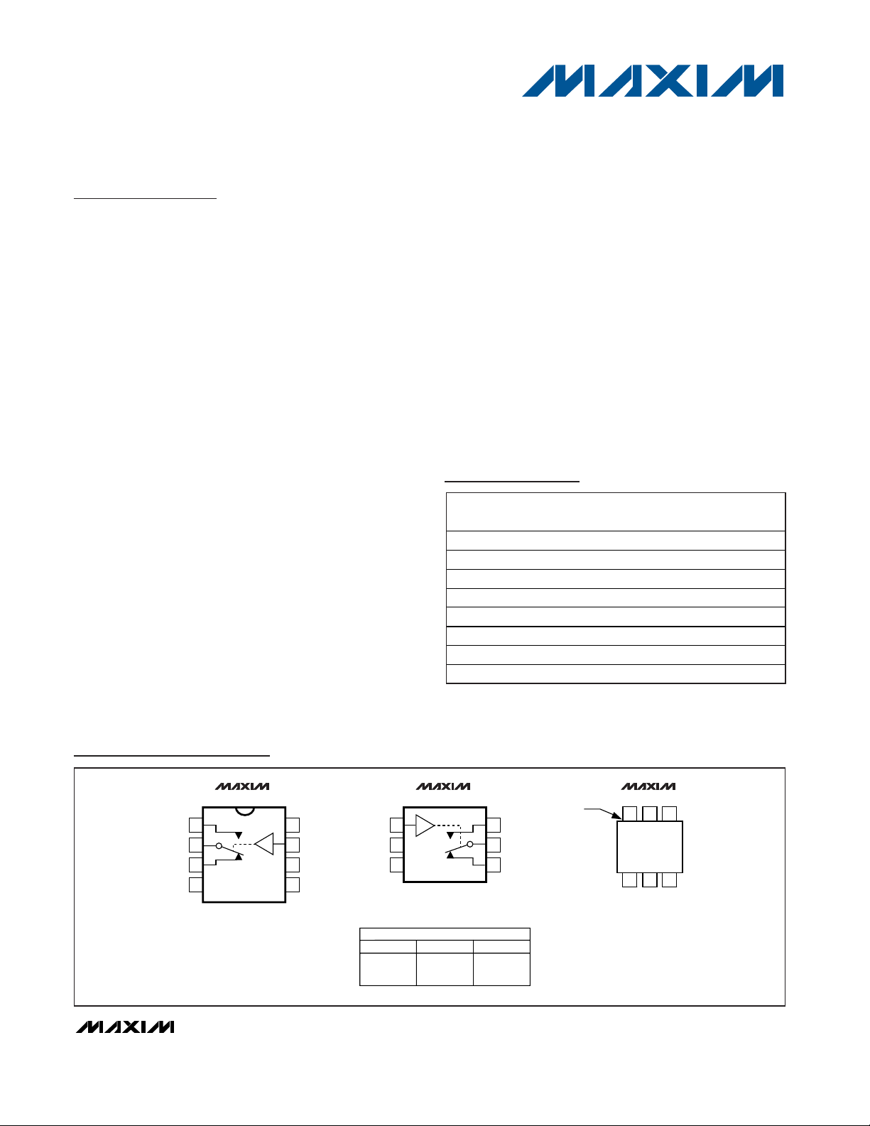
Ordering Information
Pin Configurations/Functional Diagrams/Truth Tables
μMAX/SO/DIP/TDFN
8
7
6
5
1
2
3
4
V+
PIN 6
IN
N.C.
N.C.
GND
NC
COM
NO
MAX4544
SOT23-6*
6
5
4
1
2
3
NO
COM
NC
GND
V+
IN
6
AAAM
54
123
MAX4544 MAX4544
SWITCHES SHOWN FOR "0" INPUT
N.C. = NOT INTERNALLY CONNECTED
MAX4541/MAX4542/MAX4543
APPEAR AT END OF DATA SHEET.
*NOTE: SOT23-6 PACKAGE
HAS LETTERING NEAREST PIN 6
TOP VIEW
MAX4544
LOGIC NC
0
1
ON
OFF
NO
OFF
ON
Battery-Operated Systems
Sample-and-Hold Circuits
Heads-Up Displays
Guidance and Control
Systems
Audio and Video
Switching
Military Radios
Test Equipment
Communications Systems
+3V/+5V DACs and ADCs
PBX, PABX
Cell Phones
Ultrasound
Pagers
PART
TEMP RANGE
PINPACKAGE
TOP
MARK
MAX4541CUA
8 µMAX
®
—
MAX4541CSA
8 SO —
MAX4541CPA
—
MAX4541C/D
Dice* —
MAX4541EKA-T
8 SOT23-8
AAAE
MAX4541ETA
—
MAX4541EUA
8 µMAX —
MAX4541ESA
8 SO —
µMAX is a registered trademark of Maxim Integrated Products, Inc.
0°C to +70°C
0°C to +70°C
0°C to +70°C 8 Plastic DIP
0°C to +70°C
-40°C to +85°C
-40°C to +85°C 8 TDFN-EP**
-40°C to +85°C
-40°C to +85°C
MAX4541–MAX4544
Low-Voltage, Single-Supply
Dual SPST/SPDT Analog Switches
2 _______________________________________________________________________________________
Voltage Referenced to GND
V+ .........................................................................-0.3V to +13V
IN_, COM_, NC_, NO_ (Note 1)..................-0.3V to (V+ + 0.3V)
Continuous Current (any terminal)....................................±10mA
Peak Current, COM_, NO_, NC_
(pulsed at 1ms, 10% duty cycle max) ............................±20mA
ESD per Method 3015.7 .................................................> 2000V
Continuous Power Dissipation
SOT23-6 (derate 7.1mW/°C above +70°C)....................571mW
SOT23-8 (derate 5.3mW/°C above +70°C)....................421mW
TDFN (derate 24.4mW/°C above +70°C).....................1951mW
µMAX (derate 4.10mW/°C above +70°C) ......................330mW
Narrow SO (derate 5.88mW/°C above +70°C) ..............471mW
Plastic DIP (derate 9.09mW/°C above +70°C) ..............727mW
Operating Temperature Ranges
MAX454_C_ _ .......................................................0°C to +70°C
MAX454_E_ _.....................................................-40°C to +85°C
Storage Temperature Range .............................-65°C to +150°C
Lead Temperature (soldering, 10s) .................................+300°C
Stresses beyond those listed under “Absolute Maximum Ratings” may cause permanent damage to the device. These are stress ratings only, and functional
operation of the device at these or any other conditions beyond those indicated in the operational sections of the specifications is not implied. Exposure to
absolute maximum rating conditions for extended periods may affect device reliability.
ABSOLUTE MAXIMUM RATINGS
ELECTRICAL CHARACTERISTICS—Single +5V Supply
(V+ = +5V ±10%, GND = 0, V
INH
= 2.4V, V
INL
= 0.8V, TA= T
MIN
to T
MAX
, unless otherwise noted.) (Notes 2, 3)
Note 1: Signals on NC_, NO_, COM_, or IN_ exceeding V+ or V- are clamped by internal diodes. Limit forward diode current to maximum
current rating.
COM_ On-Leakage Current
(Note 7)
I
COM(ON)
V+ = 5.5V;
V
COM_
= 1V, 4.5V or
V
NO_
or V
NC_
= 1V,
4.5V, or floating
nA
COM_ Off-Leakage Current
(Note 7)
I
COM(OFF)
V+ = 5.5V;
V
COM_
= 4.5V, 1V;
V
NO_
or V
NC_
= 1V, 4.5V
nA
NO_ or NC_ Off-Leakage
Current (Note 7)
I
NO(OFF)
or
I
NC(OFF)
V+ = 5.5V;
V
COM_
= 1V, 4.5V;
V
NO_
or V
NC_
= 4.5V, 1V
nA
-10 +10C, E
C, E
C, E
TA= T
MIN
to T
MAX
TA= T
MIN
to T
MAX
TA= T
MIN
to T
MAX
-5 +5
8
4
75
-5 +5
-0.2 +0.2
-0.1 +0.1
-0.1 ±0.01 +0.1
V+ = 5V;
I
COM_
= 1.0mA; V
NO_
or
V
NC_
= 1V, 2V, 3V
Ω
26
R
FLAT(ON)
On-Resistance Flatness
(Note 6)
V+ = 5V,
I
COM_
= 1.0mA,
V
NO_
or V
NC_
= 3.5V
Ω
0.8 2
ΔR
ON
On-Resistance Match
Between Channels (Note 5)
TA= T
MIN
to T
MAX
TA= T
MIN
to T
MAX
TA= T
MIN
to T
MAX
TA= +25°C
TA= +25°C
TA= +25°C
TA= +25°C
TA= +25°C
TA= +25°C
V+ = 4.5V,
I
COM_
= 1.0mA,
V
NO_
or V
NC_
= 3.5V
Ω
30 60
R
ON
On-Resistance
(Note 4)
CONDITIONS
V0V+
V
COM_,
V
NO_,
V
NC_
Analog Signal Range
UNITSMIN TYP MAXSYMBOLPARAMETER
ANALOG SWITCH
MAX4541–MAX4544
Low-Voltage, Single-Supply
Dual SPST/SPDT Analog Switches
_______________________________________________________________________________________ 3
ELECTRICAL CHARACTERISTICS—Single +5V Supply (continued)
(V+ = +5V ±10%, GND = 0, V
INH
= 2.4V, V
INL
= 0.8V, TA= T
MIN
to T
MAX
, unless otherwise noted.) (Notes 2, 3)
V+ = 5.5V, VIN= 0 or V+, all channels on or off µA-1 ±0.0001 +1I+Positive Supply Current
V0.8V
INL
Input-Voltage Low
V2.4V
INH
Input-Voltage High
f = 1MHz, TA= +25°C, Figure 7 pF8C
COM(OFF)
COM_ Off-Capacitance
f = 1MHz, TA= +25°C, Figure 7 pF8C
OFF
NC_ or NO_ Capacitance
RL= 50Ω, CL= 5pF, f = 1MHz, TA= +25°C,
Figure 6
dB-90Crosstalk (Note 9)
RL= 50Ω, CL= 5pF, f = 1MHz, TA= +25°C,
Figure 5
dB-76OIRROff-Isolation (Note 8)
150
240
TA= T
MIN
to T
MAX
TA= T
MIN
to T
MAX
TA= +25°C
TA= +25°C
CL= 1.0nF, V
GEN
= 0, R
GEN
= 0, TA= +25°C,
Figure 4
pC15Q
Charge Injection
(Note 4)
V2.7 12V+Power-Supply Range
V
NO_
or V
NC_
= 3V,
Figure 2
ns
25 75
t
OFF
Turn-Off Time
MAX4543/MAX4544 only, RL= 300Ω, CL= 35pF ns210t
D
Break-Before-Make Time
Delay (Note 4)
V
NO_
or V
NC_
= 3V,
Figure 2
ns
35 100
t
ON
Turn-On Time
CONDITIONS UNITSMIN TYP MAXSYMBOLPARAMETER
13
f = 1MHz, TA= +25°C,
Figure 7
pF
20
C
COM(ON)
COM_ On-Capacitance
DYNAMIC
SUPPLY
LOGIC INPUT
MAX4541/MAX4542/
MAX4543
MAX4544
MAX4541–MAX4544
Low-Voltage, Single-Supply
Dual SPST/SPDT Analog Switches
4 _______________________________________________________________________________________
ELECTRICAL CHARACTERISTICS—Single +3.3V Supply
(V+ = +3.0V to +3.6V, GND = 0, V
INH
= 2.4V, V
INL
= 0.8V, TA= T
MIN
to T
MAX
, unless otherwise noted.) (Notes 2, 3)
Note 2: QFN and SOT-packaged parts are 100% tested at +25°C only and guaranteed by correlation at the full hot rated temperature.
Note 3: The algebraic convention, where the most negative value is a minimum and the most positive value a maximum, is used in
this data sheet.
Note 4: Guaranteed by design.
Note 5: ΔR
ON
= ΔRONmax - ΔRONmin.
Note 6: Flatness is defined as the difference between the maximum and minimum value of on-resistance as measured over the
specified analog signal range.
Note 7: Leakage parameters are 100% tested at maximum rated hot temperature and guaranteed by correlation at +25°C.
Note 8: Off-isolation = 20 x log
10[VCOM
⁄ (VNCor V
NO
)
], V
COM
= output, V
NC
or VNO= input to off switch.
Note 9: Between the two switches, MAX4541/MAX4542/MAX4543 only.
PARAMETER
SYMBOL CONDITIONS MIN TYP MAX UNITS
Analog Signal Range
V
COM_,
V
NO_,
V
NC_
(Note 3) 0V+V
Channel On-Resistance R
ON
V+ = 3V,
I
COM_
= 1.0mA,
V
NO_
or V
NC_
= 1.5V
275
Turn-On Time (Note 3) t
ON
V
NO_
or V
NC_
= 1.5V
80 400
ns
500
Turn-Off Time (Note 3) t
OFF
V
NO_
or V
NC_
= 1.5V
50 125
ns
175
Break-Before-Make Time
Delay (Note 3)
t
D
MAX4543/MAX4544 only, RL= 300Ω, CL= 35pF,
TA= +25°C
230 ns
Charge Injection (Note 3) Q CL= 1.0nF, V
GEN
= 0, R
GEN
= 0, TA= +25°C 15pC
TA= T
MIN
to T
MAX
Ω
50 125TA= +25°C
TA= T
MIN
to T
MAX
TA= +25°C
TA= +25°C
TA= T
MIN
to T
MAX
Positive Supply Current I+ V+ = 3.6V, VIN= 0 or V+, all channels on or off -1 +1 µA
ANALOG SWITCH
DYNAMIC
SUPPLY
MAX4541–MAX4544
Low-Voltage, Single-Supply
Dual SPST/SPDT Analog Switches
_______________________________________________________________________________________ 5
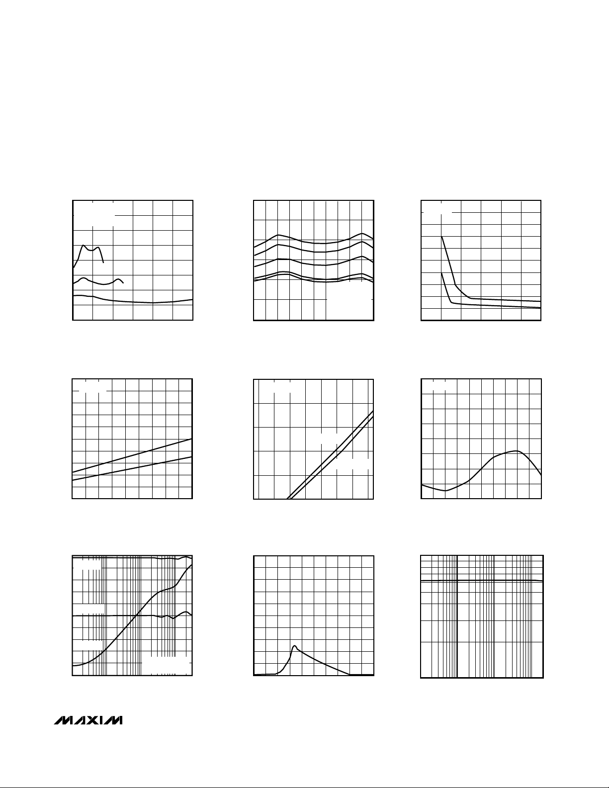
0
10
20
30
40
50
60
70
80
024681012
ON-RESISTANCE vs. COM_ VOLTAGE
MAX4541-01
V
COM_
(V)
R
ON
(Ω)
A: V+ = +3V
B: V+ = +5V
C: V+ = +12V
A
B
C
0
10
20
30
40
50
60
012345
ON-RESISTANCE vs.
COM VOLTAGE OVER TEMPERATURE
MAX4541-02
V
COM
(V)
R
ON
(Ω)
A: TA = +125°C
B: TA = +85°C
C: TA = +25°C
D: TA = -40°C
E: TA = -55°C
A
B
C
D
E
0
20
40
60
80
100
120
140
160
180
200
024681012
TURN-ON/OFF TIMES vs.
SUPPLY VOLTAGE
MAX4541-03
V
SUPPLY
(V)
t
ON
/t
OFF
(ns)
t
ON
t
OFF
V+ = +5V
0
t
ON
t
OFF
10
20
30
40
50
60
70
80
90
100
TURN-ON/OFF TIMES
vs. TEMPERATURE
MAX4541-04
TEMPERATURE (°C)
t
ON
/t
OFF
(ns)
-55 -35 -15 5 25 45 65 85 105 125
V+ = +5V
-100
-90
-80
-70
-60
-50
-40
-30
-20
-10
0
0.1 1 10 100
FREQUENCY RESPONSE
MAX4541-07
FREQUENCY (MHz)
LOSS (dB)
-225
-180
-135
-90
-45
0
45
90
135
180
225
PHASE (DEGREES)
ON-LOSS
ON-PHASE
OFF-LOSS
50Ω IN AND OUT
V+ = +5V
0.001
0.01
0.1
1
10
100
ON/OFF-LEAKAGE CURRENT
vs. TEMPERATURE
MAX4541-05
TEMPERATURE (°C)
ON/OFF-LEAKAGE (nA)
-55
-30
-5
20
45
70 95
120
125
I
COM(ON)
V+ = +5.5V
I
COM/IN(OFF)
0
1
2
3
4
5
6
7
8
012345
CHARGE INJECTION vs. COM_ VOLTAGE
MAX4541-06
V
COM_
(V)
Q (pC)
V- = +5V
0
100
200
300
400
500
600
700
800
900
1000
INPUT VOLTAGE vs. SUPPLY CURRENT
MAX4541-08
VIN (V)
I+ (nA)
012 345
I
V+
10
0.1
1
100 1k 10k
TOTAL HARMONIC DISTORTION
vs. FREQUENCY
MAX4541-09
FREQUENCY (Hz)
THD (%)
__________________________________________Typical Operating Characteristics
(TA = +25°C, unless otherwise noted.)

NAME
MAX4541–MAX4544
Low-Voltage, Single-Supply
Dual SPST/SPDT Analog Switches
6 _______________________________________________________________________________________
Applications Information
Logic Levels
The MAX4541–MAX4544 are TTL compatible when
powered from a single +5V supply. When powered
from other supply voltages, TTL compatibility is guaranteed and the logic inputs can be driven rail-to-rail.
For example, with a +12V supply, IN1 and IN2 can be
driven low to 0 and high to 12V. With a +3.3V supply,
IN1 and IN2 should be driven low to 0 and high to
3.3V.
Driving IN1 and IN2 rail-to-rail minimizes power consumption.
Analog Signal Levels
Analog signals that range over the entire supply voltage
(V+ to GND) can be switched with very little change in
on-resistance over the entire voltage range (see the
Typical Operating Characteristics). All the switches are
bidirectional, so the NO_, NC_, and COM_ pins can be
used as either inputs or outputs.
Pin Description
POSITIVE SUPPLY
COM
NO
D2
D1
GND
V
g
V+
Figure 1. Overvoltage Protection Using Two External Blocking
Diodes
Digital Control Input 1
7
2
Analog Switch 2—Common66
Analog Switch 2—Normally Open—5
Ground—Negative Supply Input44
PIN
Digital Control Input 233
Analog Switch 1—Common2
Positive Supply Voltage Input
Analog Switch 1—Normally Open11
FUNCTION
88
7
Not Connected (Open Circuit)—
—
Analog Switch—Normally Closed——
Analog Switch—Normally Open——
Analog Switch 2—Normally Closed5—
Analog Switch 1—Normally Closed—
Digital Control Input——
—
2
6
—
4
3
—
8
7
1
—
—
5
—
—
8
4
—
6
3
—
2
7
1
—
—
5
—
—
7
4
—
6
3
8
1
2
—
—
—
5
—
—
IN1
COM2
NO2
GND
IN2
COM1
NO1
NAME
V+
N.C.
NC
NO
NC2
NC1
IN
Analog Switch—Common—— — — — COM
8
4
5
6
3
1
2
7
—
—
—
—
—
—
—
—
—
—
4
—
—
—
8
5, 6
3
1
—
—
7
—
—
—
3
—
—
—
2
—
4
6
—
—
1
2 5
MAX4543
DIP/SO/
µMAX/
TDFN
MAX4541
DIP/SO/
µMAX/
TDFN
SOT23-8
DIP/SO/
µMAX/
TDFN
MAX4542
SOT23-8 SOT23-8
DIP/SO/
µMAX/
TDFN
MAX4544
SOT23-6
Exposed Pad. Connect EP to V+.EPEP EP — — EP— EP —

Power-Supply Sequencing
and Overvoltage Protection
Do not exceed the absolute maximum ratings because
stresses beyond the listed ratings may cause permanent damage to the devices.
Proper power-supply sequencing is recommended for
all CMOS devices. Always apply V+ before applying
analog signals or logic inputs, especially if the analog
or logic signals are not current limited. If this sequencing is not possible, and if the analog or logic inputs are
not current limited to < 10mA, add a small-signal diode
(D1) as shown in Figure 1. If the analog signal can dip
below GND, add D2. Adding protection diodes
reduces the analog signal range to a diode drop (about
0.7V) below V+ (for D1), and to a diode drop above
ground (for D2). Leakage is unaffected by adding the
diodes. On-resistance increases by a small amount at
low supply voltages. Maximum supply voltage (V+)
must not exceed 13V.
Adding protection diodes causes the logic thresholds
to be shifted relative to the power-supply rails. This can
be significant when low supply voltages (+5V or less)
are used. With a +5V supply, TTL compatibility is not
guaranteed when protection diodes are added. Driving
IN1 and IN2 all the way to the supply rails (i.e., to a
diode drop higher than the V+ pin, or to a diode drop
lower than the GND pin) is always acceptable.
Protection diodes D1 and D2 also protect against
some overvoltage situations. With Figure 1’s circuit, if
the supply voltage is below the absolute maximum rating, and if a fault voltage up to the absolute maximum
rating is applied to an analog signal pin, no damage
will result.
MAX4541–MAX4544
Low-Voltage, Single-Supply
Dual SPST/SPDT Analog Switches
_______________________________________________________________________________________ 7
tr < 20ns
tf < 20ns
50%
0
LOGIC
INPUT
R
L
1kΩ
COM
GND
C
L
INCLUDES FIXTURE AND STRAY CAPACITANCE.
V
OUT
= V
COM (
R
L
)
RL + R
ON
SWITCH
INPUT
IN
+3V
t
OFF
0
NO
or NC
SWITCH
OUTPUT
0.9 x V
0UT
0.9 x V
OUT
t
ON
V
OUT
SWITCH
OUTPUT
LOGIC
INPUT
LOGIC INPUT WAVEFORMS INVERTED FOR SWITCHES
THAT HAVE THE OPPOSITE LOGIC SENSE.
V+
C
L
35pF
V+
V
OUT
0V
MAX4541
MAX4542
MAX4543
MAX4544
Figure 2. Switching Time
Test Circuits/Timing Diagrams

MAX4541–MAX4544
Low-Voltage, Single-Supply
Dual SPST/SPDT Analog Switches
8 _______________________________________________________________________________________
V
GEN
GND
COM
C
L
V
OUT
V+
V
OUT
IN
OFF
ON
OFF
ΔV
OUT
Q = (ΔV
OUT
)(CL)
NC
OR NO
IN DEPENDS ON SWITCH CONFIGURATION;
INPUT POLARITY DETERMINED BY SENSE OF SWITCH.
OFF
ON
OFF
IN
V
IN
= +3V
V+
R
GEN
IN_
MAX4541
MAX4542
MAX4543
MAX4544
Figure 4. Charge Injection
50%
0.9
x V
0UT1
+3V
0
0
LOGIC
INPUT
SWITCH
OUTPUT 2
(V
OUT2
)
0
0.9 x V
OUT2
t
D
t
D
LOGIC
INPUT
R
L2
300Ω
GND
C
L
INCLUDES FIXTURE AND STRAY CAPACITANCE.
NC2
IN2
IN1
NO1
V
OUT2
V+
V+
C
L2
35pF
+3V
R
L1
300Ω
V
OUT1
C
L1
35pF
COM1
COM2
SWITCH
OUTPUT 1
(V
OUT1
)
MAX4543
Figure 3a. Break-Before-Make Interval (MAX4543 Only)
Figure 3b. Break-Before-Make Interval (MAX4544 Only)
_________________________________Test Circuits/Timing Diagrams (continued)
GND
V+
V+
V
R
L
300Ω
OUT
C
L
35pF
COM
LOGIC
INPUT
SWITCH
OUTPUT
(V
OUT
+3V
0
)
MAX4544
+3V
LOGIC
INPUT
NC
NO
IN
INCLUDES FIXTURE AND STRAY CAPACITANCE.
C
L
50%
t
D
0.9 x V
OUT

MAX4541–MAX4544
Low-Voltage, Single-Supply
Dual SPST/SPDT Analog Switches
_______________________________________________________________________________________ 9
Figure 6. Crosstalk
IN
0V OR
2.4V
SIGNAL
GENERATOR 0dBm
V+
10nF
ANALYZER
NC
OR NO
R
L
GND
COM
V+
MAX4541
MAX4542
MAX4543
MAX4544
Figure 5. Off-Isolation
_________________________________Test Circuits/Timing Diagrams (continued)
CAPACITANCE
METER
NC OR
NO
COM
GND
IN
0 OR
2.4V
10nF
V+
f = 1MHz
V+
MAX4541
MAX4542
MAX4543
MAX4544
Figure 7. Channel Off/On-Capacitance
NO1
IN2
COM2
MAX4541
MAX4542
MAX4543
50Ω
0 OR
2.4V
NC
SIGNAL
GENERATOR 0dBm
0 OR 2.4V
ANALYZER
R
L
10nF
V+
V+
COM1
IN1
NO2
GND

MAX4541–MAX4544
Low-Voltage, Single-Supply
Dual SPST/SPDT Analog Switches
10 ______________________________________________________________________________________
___Ordering Information (continued)
*Dice are specified at TA= +25°C.
**EP = Exposed pad.
PART
TEMP RANGE
PINPACKAGE
TOP
MARK
MAX4541EPA
—
MAX4542CUA
8 µMAX —
MAX4542CSA
8 SO —
MAX4542CPA
—
MAX4542C/D
Dice* —
MAX4542EKA-T
8 SOT23-8
AAAF
MAX4542ETA
—
MAX4542EUA
8 µMAX —
MAX4542ESA
8 SO —
MAX4542EPA
—
MAX4543CUA
8 µMAX —
MAX4543CSA
8 SO —
MAX4543CPA
—
MAX4543C/D
Dice* —
MAX4543EKA-T
8 SOT23-8
AAAG
MAX4543ETA
—
MAX4543EUA
8 µMAX —
MAX4543ESA
8 SO —
MAX4543EPA
—
MAX4544CUA
8 µMAX —
MAX4544CSA
8 SO —
MAX4544CPA
—
MAX4544C/D
Dice* —
MAX4544EUT-T
6 SOT23-6
AAAM
MAX4544ETA
—
MAX4544EUA
8 µMAX —
MAX4544ESA
8 SO —
MAX4544EPA
—
-40°C to +85°C 8 Plastic DIP
0°C to +70°C
0°C to +70°C
0°C to +70°C 8 Plastic DIP
0°C to +70°C
-40°C to +85°C
-40°C to +85°C 8 TDFN-EP**
-40°C to +85°C
-40°C to +85°C
-40°C to +85°C 8 Plastic DIP
0°C to +70°C
0°C to +70°C
0°C to +70°C 8 Plastic DIP
0°C to +70°C
-40°C to +85°C
-40°C to +85°C 8 TDFN-EP**
-40°C to +85°C
-40°C to +85°C
-40°C to +85°C 8 Plastic DIP
0°C to +70°C
0°C to +70°C
0°C to +70°C 8 Plastic DIP
0°C to +70°C
-40°C to +85°C
-40°C to +85°C 8 TDFN-EP**
-40°C to +85°C
-40°C to +85°C
-40°C to +85°C 8 Plastic DIP

MAX4541–MAX4544
Low-Voltage, Single-Supply
Dual SPST/SPDT Analog Switches
______________________________________________________________________________________ 11
μMAX/SO/DIP/TDFN
8
7
6
5
1
2
3
4
V+
IN1
COM2
NC2
GND
IN2
COM1
NC1
MAX4542
μMAX/SO/DIP/TDFN
8
7
6
5
1
2
3
4
V+
IN1
COM2
NC2
GND
IN2
COM1
NO1
MAX4543
SWITCHES SHOWN FOR LOGIC "0" INPUT
TOP VIEW
μMAX/SO/DIP/TDFN
8
7
6
5
1
2
3
4
V+
IN1
COM2
NO2
GND
IN2
COM1
NO1
MAX4541
SOT23-8
8
7
6
5
1
2
3
4
COM1
IN1
GND
NC2
COM2
IN2
V+
NC1
MAX4542
SOT23-8
8
7
6
5
1
2
3
4
COM1
IN1
GND
NC2
COM2
IN2
V+
NO1
MAX4543
SOT23-8
8
7
6
5
1
2
3
4
COM1
IN1
GND
NO2
COM2
IN2
V+
NO1
MAX4541
_________Pin Configurations/Functional Diagrams/Truth Tables (continued)

MAX4541–MAX4544
Low-Voltage, Single-Supply
Dual SPST/SPDT Analog Switches
12 ______________________________________________________________________________________
6, 8, &10L, DFN THIN.EPS
Package Information
(The package drawing(s) in this data sheet may not reflect the most current specifications. For the latest package outline information
go to www.maxim-ic.com/packages
.)

MAX4541–MAX4544
Low-Voltage, Single-Supply
Dual SPST/SPDT Analog Switches
______________________________________________________________________________________ 13
COMMON DIMENSIONS
SYMBOL MIN. MAX.
A 0.70 0.80
D 2.90 3.10
E 2.90 3.10
A1
0.00 0.05
L 0.20 0.40
PKG. CODE N D2 E2 e JEDEC SPEC b
[(N/2)-1] x e
PACKAGE VARIATIONS
0.25 MIN.k
A2 0.20 REF.
2.00 REF0.25±0.050.50 BSC2.30±0.1010T1033-1
2.40 REF0.20±0.05- - - - 0.40 BSC1.70±0.10 2.30±0.1014T1433-1
1.50±0.10 MO229 / WEED-3
0.40 BSC - - - - 0.20±0.05 2.40 REFT1433-2 14 2.30±0.101.70±0.10
T633-2 6 1.50±0.10 2.30±0.10 0.95 BSC MO229 / WEEA 0.40±0.05 1.90 REF
T833-2 8 1.50±0.10 2.30±0.10 0.65 BSC MO229 / WEEC 0.30±0.05 1.95 REF
T833-3 8 1.50±0.10 2.30±0.10 0.65 BSC MO229 / WEEC 0.30±0.05 1.95 REF
2.30±0.10 MO229 / WEED-3 2.00 REF0.25±0.050.50 BSC1.50±0.1010T1033-2
Package Information (continued)
(The package drawing(s) in this data sheet may not reflect the most current specifications. For the latest package outline information
go to www.maxim-ic.com/packages
.)

MAX4541–MAX4544
Low-Voltage, Single-Supply
Dual SPST/SPDT Analog Switches
14 ______________________________________________________________________________________
6LSOT.EPS
PACKAGE OUTLINE, SOT 6L BODY
21-0058
2
1
I
Package Information (continued)
(The package drawing(s) in this data sheet may not reflect the most current specifications. For the latest package outline information
go to www.maxim-ic.com/packages
.)

MAX4541–MAX4544
Low-Voltage, Single-Supply
Dual SPST/SPDT Analog Switches
______________________________________________________________________________________ 15
PACKAGE OUTLINE, SOT 6L BODY
21-0058
2
2
I
Package Information (continued)
(The package drawing(s) in this data sheet may not reflect the most current specifications. For the latest package outline information
go to www.maxim-ic.com/packages
.)

Package Information (continued)
(The package drawing(s) in this data sheet may not reflect the most current specifications. For the latest package outline information
go to www.maxim-ic.com/packages
.)
Revision History
Pages changed at Rev 4: 1–16
MAX4541–MAX4544
Low-Voltage, Single-Supply
Dual SPST/SPDT Analog Switches
Maxim cannot assume responsibility for use of any circuitry other than circuitry entirely embodied in a Maxim product. No circuit patent licenses are
implied. Maxim reserves the right to change the circuitry and specifications without notice at any time.
16 ____________________Maxim Integrated Products, 120 San Gabriel Drive, Sunnyvale, CA 94086 408-737-7600
© 2007 Maxim Integrated Products is a registered trademark of Maxim Integrated Products, Inc.
MARKING
0
SOT23, 8L.EPS
0
PACKAGE OUTLINE, SOT-23, 8L BODY
21-0078 G
1
1
 Loading...