

Page 1
General Description
The MAX4539/MAX4540 low-voltage, CMOS 8-channel
(MAX4539) and dual 4-channel (MAX4540) multiplexers
are ideal for precision ADC calibration and system selfmonitoring applications. These calibration multiplexers
(cal-muxes) have precision resistor-dividers to generate
accurate voltage ratios from an input reference voltage.
The reference ratios include 15/4096 and 4081/4096 of
the external reference voltage, accurate to 15 bits, and
1/2V+ and 5/8(V+ - V-), accurate to 8 bits. The external
reference voltage as well as ground can also be
switched to the output. The MAX4539/MAX4540 have
enable inputs and address latching. All digital inputs
have 0.8V and 2.4V logic thresholds, ensuring both
TTL- and CMOS-logic compatibility when using a ±5V
or a single +5V supply. Protection diodes at all inputs
provide an ESD rating >2kV.
The MAX4539/MAX4540 operate from a single +2.7V to
+12V supply, or from dual supplies of ±2.7V to ±6V.
On-resistance (100Ω max) is matched between switches to 6Ω max. Each switch can handle Rail-to-Rail
®
analog signals. The off leakage current is 0.1nA at
TA= +25°C and 2nA at TA= +85°C.
The MAX4539/MAX4540 are available in small 20-pin
DIP, SO, and SSOP packages.
Applications
Battery-Operated Equipment Avionics
Data-Acquisition Systems Audio-Signal Routing
Test Equipment Networking
Features
♦ On-Chip Gain and Offset Divider Networks
Provide 15-Bit Accurate Output Ratios
♦ On-Chip V+ to GND and V+ to V- Divider Networks
Provide 8-Bit Accurate Output Ratios
♦ RON: 100Ω max
♦ R
ON
Matching Between Channels: 6Ω max
♦ Charge Injection: 5pC max
♦ Low 0.1nA Off Leakage Current
♦ Small 20-Pin SSOP/SO/DIP Packages
MAX4539/MAX4540
Low-Voltage, Single 8-to-1 and
Dual 4-to-1 Cal-Multiplexers
________________________________________________________________
Maxim Integrated Products
1
19-4780; Rev 1; 6/99
PART
MAX4539CAP
MAX4539CWP
MAX4539CPP 0°C to +70°C
0°C to +70°C
0°C to +70°C
TEMP. RANGE PIN-PACKAGE
20 SSOP
20 Wide SO
20 Plastic DIP
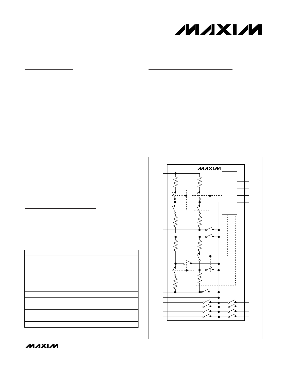
Pin Configurations/
_______________Functional Diagrams
Ordering Information
Rail-to-Rail is a registered trademark of Nippon Motorola, Ltd.
MAX4539EAP
MAX4539EWP -40°C to +85°C
-40°C to +85°C 20 SSOP
20 Wide SO
MAX4539EPP -40°C to +85°C 20 Plastic DIP
MAX4540CAP
MAX4540CWP
MAX4540CPP 0°C to +70°C
0°C to +70°C
0°C to +70°C 20 SSOP
20 Wide SO
20 Plastic DIP
MAX4540EAP
MAX4540EWP -40°C to +85°C
-40°C to +85°C 20 SSOP
20 Wide SO
MAX4540EPP -40°C to +85°C 20 Plastic DIP
MAX4540 appears at end of data sheet.
For free samples & the latest literature: http://www.maxim-ic.com, or phone 1-800-998-8800.
For small orders, phone 1-800-835-8769.
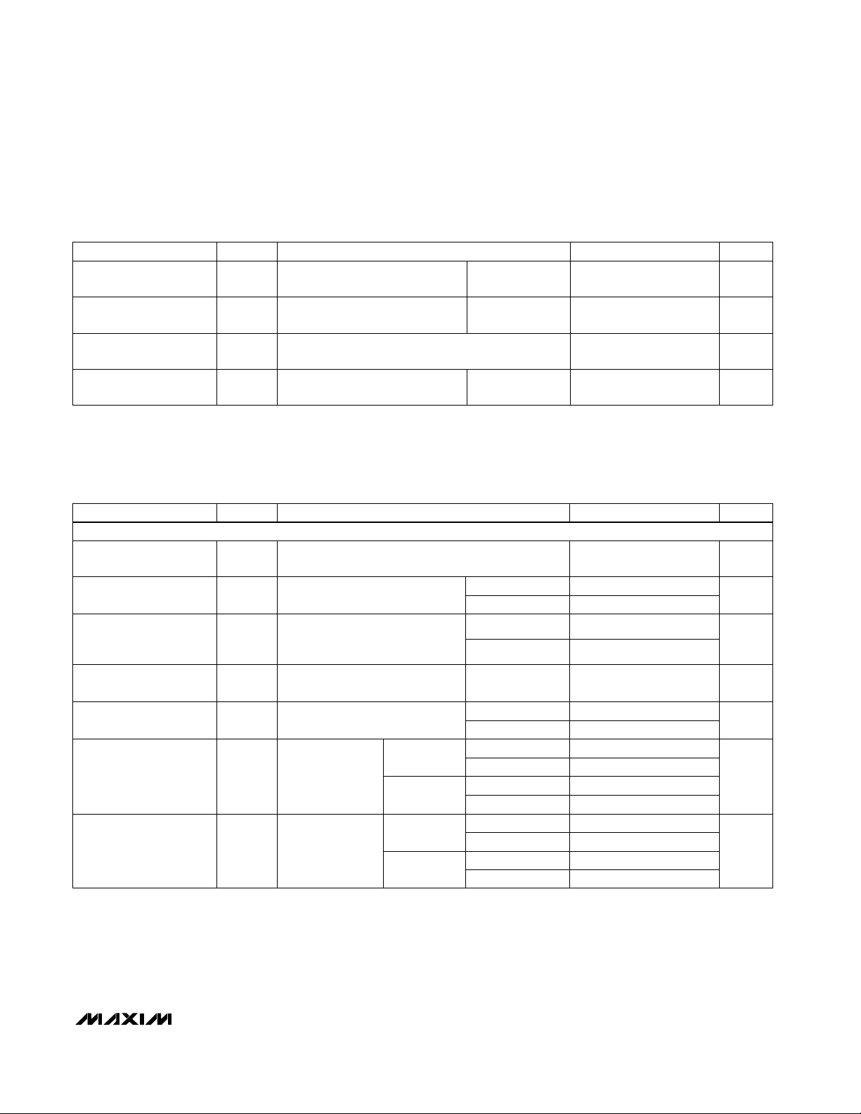
GND
REFHI
1
V+
5R R2
2
3
V-
4
MAX4539
R23R
DECODER
LOGIC
20
LATCH
19
EN
18
CAL
17
A0
16
A1
15
A2
15R1
4081R1
4081R1
REFLO
5
6
COM
7
NO1
8
NO2
9
NO3
10
NO4
15R1
14
NO8
13
NO7
12
NO6
11
NO5
Page 2
MAX4539/MAX4540
Low-Voltage, Single 8-to-1 and
Dual 4-to-1 Cal-Multiplexers
2 _______________________________________________________________________________________
ABSOLUTE MAXIMUM RATINGS
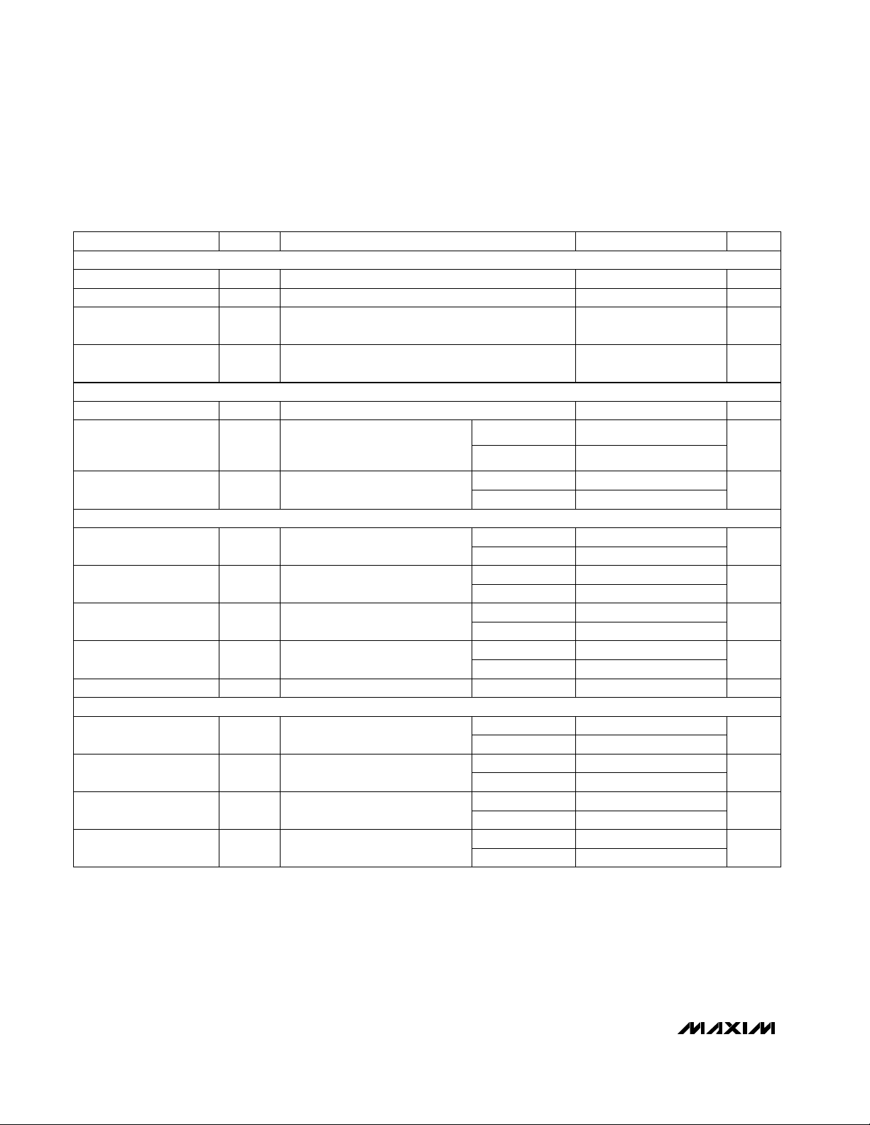
ELECTRICAL CHARACTERISTICS—Dual Supplies
(V+ = +5V ±10%, V- = -5V ±10%, VIH= 2.4V, VIL= 0.8V, TA= T
MIN
to T
MAX
, unless otherwise noted. Typical values at TA= +25°C.)
(Note 2)
Stresses beyond those listed under “Absolute Maximum Ratings” may cause permanent damage to the device. These are stress ratings only, and functional
operation of the device at these or any other conditions beyond those indicated in the operational sections of the specifications is not implied. Exposure to
absolute maximum rating conditions for extended periods may affect device reliability.
Note 1: Signals on NO_, COM_, EN, LATCH, CAL, A_ exceeding V+ or V- are clamped by internal diodes. Limit forward current to
maximum current ratings.
V+ to GND..............................................................-0.3V to +13V
V- to GND ...............................................................-13V to +0.3V
V+ to V-...................................................................-0.3V to +13V
CAL, LATCH, A_, EN, NO_, COM_,
REFHI, REFLO (Note 1) ........................(V- - 0.3V) to (V+ + 0.3V)
Continuous Current (any terminal)....................................±20mA
Peak Current, NO_ or COM_
(pulsed at 1ms, 10% duty cycle max)...........................±40mA
Continuous Power Dissipation (T
A
= +70°C)
SSOP (derate 8mW/°C above +70°C) ..........................640mW
Wide SO (derate 8mW/°C above +70°C)......................800mW
Plastic DIP (derate 10.53mW/°C above +70°C) ...........842mW
Operating Temperature Ranges
MAX4539C_P/MAX4540C_P................................0°C to +70°C
MAX4539E_P/MAX4540E_P .............................-40°C to +85°C
Storage Temperature Range .............................-65°C to +160°C
Lead Temperature (soldering, 10sec) ............................+300° C
(Note 3)
I
COM_
= 1mA; V
NO_
= -3V, 0, +3V;
V+ = 4.5V; V- = -4.5V
I
COM_
= 1mA, V
NO_
= ±3.0V,
V+ = 4.5V, V- = -4.5V
I
COM_
= 1mA, V
NO_
= ±3.0V,
V+ = 4.5V, V- = -4.5V
CONDITIONS
45 75
VV- V+
V
COM_
,
V
NO_
Analog-Signal Range
Ω
13
R
FLAT
Ω
100
R
ON
On-Resistance
14
Ω
6
∆R
ON
710
On-Resistance Flatness
(Note 5)
UNITSMIN TYP MAXSYMBOLPARAMETER
On-Resistance Matching
Between Channels
(Note 4)
V
COM_
= ±4.5V, V
NO_
= 4.5V,
V+ = 5.5V, V- = -5.5V
nA
-2 2
I
NO(OFF)
-0.1 0.01 0.1
NO-Off Leakage Current
(Note 6)
-10 10
V
COM_
= ±4.5V,
V
NO_
= 4.5V,
V+ = 5.5V,
V- = -5.5V
-0.2 0.01 0.2
nA
-5 5
I
COM_(OFF)
-0.1 0.01 0.1
COM-Off Leakage
Current (Note 6)
TA= +25°C
TA= T
MIN
to T
MAX
TA= +25°C
TA= T
MIN
to T
MAX
TA= +25°C
TA= T
MIN
to T
MAX
TA= +25°C
TA= T
MIN
to T
MAX
TA= +25°C
MAX4539
TA= T
MIN
to T
MAX
TA= +25°C
TA= T
MIN
to T
MAX
MAX4540
-10 10
-0.2 0.01 0.2
nA
-5 5
I
COM_(ON)
-0.1 0.01 0.1
COM-On Leakage
Current (Note 6)
TA= +25°C
TA= T
MIN
to T
MAX
MAX4539
TA= +25°C
TA= T
MIN
to T
MAX
MAX4540
V
COM_
= ±4.5V,
V
NO_
= ±4.5V,
V+ = 5.5V,
V- = -5.5V
SWITCH
±
±
Page 3
MAX4539/MAX4540
Low-Voltage, Single 8-to-1 and
Dual 4-to-1 Cal-Multiplexers
_______________________________________________________________________________________ 3
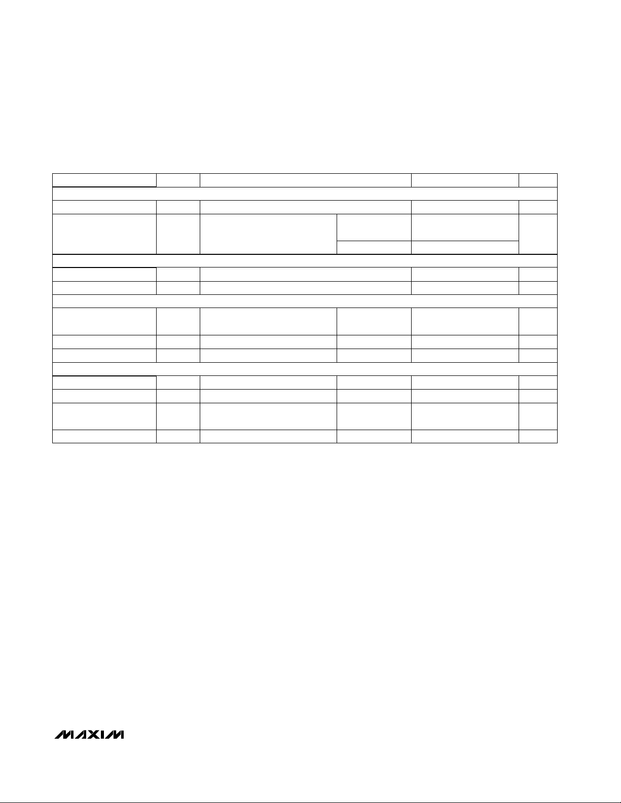
CONDITIONS
VEN= VA_= V
LATCH
= V
CAL
= V+ µA-0.1 0.01 0.1I
IH
Input Current with Input
Voltage High
V1.4 0.8V
IL
Input Low Voltage
V2.4 1.7V
IH
Input High Voltage
UNITSMIN TYP MAXSYMBOLPARAMETER
ELECTRICAL CHARACTERISTICS—Dual Supplies (continued)
(V+ = +5V ±10%, V- = -5V ±10%, VIH= 2.4V, VIL= 0.8V, TA= T
MIN
to T
MAX
, unless otherwise noted. Typical values at TA= +25°C.)
(Note 2)
VEN= VA_= V
LATCH
= V
CAL
= 0
or V+, V+ = 5.5V, V- = -5.5V
(Note 7)
µA
-5 5
I+Positive Supply Current
-1 0.01 1
V±2.7 ±6Power-Supply Range
VEN= VA_= V
LATCH
= V
CAL
= 0 µA-0.1 0.01 0.1I
IL
Input Current with Input
Voltage Low
Figure 2 ns
410
t
OPEN
Break-Before-Make
Interval (Note 3)
100 150
TA= +25°C
TA= T
MIN
to T
MAX
VEN= VA_= V
LATCH
= V
CAL
= 0
or V+, V+ = 5.5V, V- = -5.5V
(Note 7)
TA= T
MIN
to T
MAX
µA
-5 5
I-Negative Supply Current
-1 0.01 1TA= +25°C
VEN= VA_= V
LATCH
= V
CAL
= 0
or V+, V+ = 5.5V, V- = -5.5V
(Note 7)
TA= T
MIN
to T
MAX
µA
-5 5
I
GND
GND Supply Current
-1 0.01 1TA= +25°C
TA= +25°C
TA= +25°C
50 100
75 115TA= +25°C
TA= +25°C
VEN= 0, f = 1MHz, Figure 5
CL= 1nF, V
NO_
= 0, Figure 4
dB-75V
ISO
Off-Isolation (Note 8)
pC15V
CTE
Charge Injection
(Note 3)
TA= +25°C
TA= +25°C
f = 1MHz
VEN= 2.4V, f = 1MHz,
V
GEN
= 1Vp-p, Figure 5
pF15C
IN
Logic Input Capacitance
dB-75V
CT
Crosstalk Between
Channels (Note 9)
TA= +25°C
TA= +25°C
f = 1MHz, VEN= V
COM_
= 0,
Figure 6
pF3C
OFF
NO-Off Capacitance TA= +25°C
f = 1MHz, VEN= 2.4V,
V
COM_
= 0, Figure 6
f = 1MHz, VEN= V
COM_
= 0,
Figure 6
pF26C
COM_(ON)
COM-On Capacitance
pF15C
COM_(OFF)
COM-Off Capacitance TA= +25°C
TA= +25°C
Figure 3 ns
175
t
ON
Enable Turn-On Time
TA= T
MIN
to T
MAX
Figure 3 ns
120
t
OFF
Enable Turn-Off Time
TA= T
MIN
to T
MAX
TA= T
MIN
to T
MAX
Figure 1 ns
200
t
TRANS
Transition Time
TA= T
MIN
to T
MAX
1
LOGIC INPUTS
SUPPLY
DYNAMIC CHARACTERISTICS
Page 4
MAX4539/MAX4540
Low-Voltage, Single 8-to-1 and
Dual 4-to-1 Cal-Multiplexers
4 _______________________________________________________________________________________
ELECTRICAL CHARACTERISTICS—Dual Supplies (continued)
(V+ = +5V ±10%, V- = -5V ±10%, VIH= 2.4V, VIL= 0.8V, TA= T
MIN
to T
MAX
, unless otherwise noted. Typical values at TA= +25°C.)
(Note 2)
TA= +25°C
Additional Positive Supply
Current
V+ / V+ /
24k 13k
(V+ / 2) divider active,
V
IH
= V+, V
IL
= 0 (Note 3)
TA= T
MIN
to T
MAX
Enable Setup Time t
ES
40
nsFigure 8
TA= +25°C 15 30
TA= T
MIN
to T
MAX
(V+ - V-) Divider Output
2544/ 2560/ 2576/
4096 4096 4096
Referenced to V- LSB
TA= +25°C
2544/ 2560/ 2576/
4096 4096 4096
TA= T
MIN
to T
MAX
(V+ / 2) Divider Output
2032/ 2048/ 2064/
4096 4096 4096
Referenced to GND LSB
TA= +25°C
2032/ 2048/ 2064/
4096 4096 4096
TA= T
MIN
to T
MAX
Gain Divider Output
4080.9/ 4081/ 4081.1/
4096 4096 4096
V
REF
= 4.096V,
REFHI = 4.096V,
REFLO = GND
LSB
TA= +25°C
4080.9/ 4081/ 4081.1/
4096 4096 4096
TA= T
MIN
to T
MAX
Offset Divider Output
14.9/ 15/ 15.1/
4096 4096 4096
V
REF
= 4.096V,
REFHI = 4.096V,
REFLO = GND
TA= +25°C
Output Resistance
(V+ - V-) Divider
69kΩ(Note 3)
TA= +25°C
Output Resistance Gain
Divider
400 800 Ω(Note 3)
LSB
TA= +25°C
14.9/ 15/ 15.1/
4096 4096 4096
TA= T
MIN
to T
MAX
Pulse Width, Latch
Enable
t
MPW
40
nsFigure 7
TA= T
MIN
to T
MAX
Setup Time t
S
PARAMETER SYMBOL MIN TYP MAX UNITS
TA= +25°C
Output Resistance
(REFHI, REFLO, GND)
400 800 Ω(Note 3)
TA= +25°C
Output Resistance
(V+ / 2) Divider
69kΩ(Note 3)
TA= +25°C
Output Resistance Offset
Divider
400 800 Ω(Note 3)
TA= +25°C
80
ns
TA= T
MIN
to T
MAX
Figure 7
30 15
TA= +25°C
TA= +25°C 45 70
Hold Time t
H
-10 0
ns
-10
Figure 7
CONDITIONS
mA
LATCH TIMING (Note 3)
INTERNAL DIVIDERS
Page 5
TA= T
MIN
to T
MAX
MAX4539/MAX4540
Low-Voltage, Single 8-to-1 and
Dual 4-to-1 Cal-Multiplexers
_______________________________________________________________________________________ 5
ELECTRICAL CHARACTERISTICS—Dual Supplies (continued)
(V+ = +5V ±10%, V- = -5V ±10%, VIH= 2.4V, VIL= 0.8V, TA= T
MIN
to T
MAX
, unless otherwise noted. Typical values at TA= +25°C.)
(Note 2)
ELECTRICAL CHARACTERISTICS—Single +5V Supply
(V+ = +5V ±10%, V- = 0, VIH= 2.4V, VIL= 0.8V, TA= T
MIN
to T
MAX
, unless otherwise noted. Typical values at TA= +25°C.) (Note 2)
-10 10
-0.2 0.2
TA= +25°C
-10 10
TA= T
MIN
to T
MAX
(Note 3)
V
COM_
= 4.5V, 1V;
V
NO_
= 1V, 4.5V;
V+ = 5.5V
nA
-5 5
-0.2 0.2
TA= +25°C
I
COM_
= 1mA; V
NO_
= 3V, 2V, 1V;
V+ = 4.5V
I
COM_
= 1mA, V
NO_
= 3.0V,
V+ = 4.5V
TA= +25°C
I
COM_
= 1mA, V
NO_
= 3.0V,
V+ = 4.5V
nA
TA= T
MIN
to T
MAX
-5 5
CONDITIONS
I
COM_(OFF)
I
COM_(ON)
-0.1 0.1
TA= T
MIN
to T
MAX
COM-Off Leakage
Current (Notes 6, 10)
TA= +25°C
V
COM_
= 4.5V,
V
NO_
= 4.5V,
V+ = 5.5V
TA= +25°C
TA= T
MIN
to T
MAX
MAX4539
-0.1 0.1
TA= +25°C
COM-On Leakage
Current (Notes 6, 10)
TA= T
MIN
to T
MAX
MAX4540
TA= +25°C
TA= T
MIN
to T
MAX
MAX4539
TA= +25°C
TA= T
MIN
to T
MAX
MAX4540
80 150
V0V+
V
NO_
,
V
COM_
Analog-Signal Range
ΩR
FLAT
V
COM_
= 1V, 4.5V;
V
NO_
= 4.5V, 1V; V+ = 5.5V
Ω
200
R
ON
On-Resistance
28
On-Resistance Matching
Between Channels
(Notes 3, 4)
Ω
12
∆R
ON
8
On-Resistance Flatness
(Note 5)
UNITSMIN TYP MAXSYMBOLPARAMETER
nA
-2 2
I
NO(OFF)
-0.1 0.1
NO-Off Leakage Current
(Notes 6, 10)
SWITCH
TA= +25°C
Additional Negative
Supply Current
(V+ - V-)/ (V+ - V-)/
24k 13k
mA
(V+ - V-) divider active,
V
IH
= V+, VIL= 0 (Note 3)
TA= +25°C
Additional Positive Supply
Current (Note 3)
(V+ - V-)/ (V+ - V-)/
24k 13k
mA
PARAMETER SYMBOL MIN TYP MAX UNITS
(V+ - V-) divider active,
V
IH
= V+, VIL= 0
TA= +25°C
Input Resistance
(REFHI, REFLO) (Note 3)
25 40 kΩ
Offset divider active,
gain divider active
REFHI, REFLO Input
Range (Note 3)
V- V+
- 0.3 + 0.3
V
CONDITIONS
Page 6
MAX4539/MAX4540
Low-Voltage, Single 8-to-1 and
Dual 4-to-1 Cal-Multiplexers
6 _______________________________________________________________________________________
ELECTRICAL CHARACTERISTICS—Single +5V Supply (continued)
(V+ = +5V ±10%, V- = 0, VIH= 2.4V, VIL= 0.8V, TA= T
MIN
to T
MAX
, unless otherwise noted. Typical values at TA= +25°C.) (Note 2)
VEN= VA_= V
LATCH
= V
CAL
= 0
or V+, V+ = 5.5V
TA= T
MIN
to T
MAX
µA
-5 5
I+
Positive Supply Current
(Note 3)
-1 0.01 1
V2.7 12Power-Supply Range
VEN= VA_= V
LATCH
= V
CAL
= 0
CONDITIONS
µA-0.1 0.1I
IL
Input Current with
Input Voltage Low
VEN= VA_= V
LATCH
= V
CAL
= V+
Figure 2
1
ns
410
t
OPEN
Break-Before-Make
Interval
µA-0.1 0.1I
IH
Input Current with
Input Voltage High
150 200
TA= +25°C
VEN= VA_= V
LATCH
= V
CAL
= 0
or V+, V+ = 5.5V
TA= T
MIN
to T
MAX
µA
-10 10
I
GND
GND Supply Current
(Note 3)
-1 0.01 1TA= +25°C
TA= +25°C
TA= +25°C
60 100
Figure 1
TA= T
MIN
to T
MAX
115 150
ns
250
TA= +25°C
TA= +25°C
CL= 1nF, V
NO_
= 0, Figure 4 pC15V
CTE
Charge Injection TA= +25°C
V1.4 0.8V
IL
Input Low Voltage
V2.4 1.6V
IH
Input High Voltage
70TA= +25°C
UNITSMIN TYP MAXSYMBOLPARAMETER
t
TRANS
Transition Time
TA= T
MIN
to T
MAX
Figure 3 ns
200
t
ON
Enable Turn-On Time
TA= T
MIN
to T
MAX
Figure 3 ns
130
t
OFF
Enable Turn-Off Time
TA= T
MIN
to T
MAX
Figure 7
80
t
S
Setup Time
TA= T
MIN
to T
MAX
Figure 7 ns
-10
t
H
Hold Time
TA= T
MIN
to T
MAX
-10 0TA= +25°C
Figure 7 ns
40
t
MPW
TA= T
MIN
to T
MAX
30 15
Pulse Width, Latch
Enable
TA= +25°C
ns
Figure 8 ns
40
t
ES
TA= T
MIN
to T
MAX
15 30
Enable Setup Time
TA= +25°C
LOGIC INPUTS (Note 3)
SUPPLY
DYNAMIC CHARACTERISTICS (Note 3)
LATCH TIMING (Note 3)
Page 7
MAX4539/MAX4540
Low-Voltage, Single 8-to-1 and
Dual 4-to-1 Cal-Multiplexers
_______________________________________________________________________________________ 7
Note 2: The algebraic convention, where the most negative value is a minimum and the most positive value a maximum, is used in
this data sheet.
Note 3: Guaranteed by design.
Note 4: ∆R
ON
= R
ON(MAX)
- R
ON(MIN)
.
Note 5: Flatness is defined as the difference between the maximum and minimum value of on-resistance as measured over the
specified analog signal range.
Note 6: Leakage parameters are 100% tested at maximum-rated hot temperature and guaranteed by correlation at T
A
= +25°C.
Note 7: If the logic inputs can float during power-on, connect a 1MΩ pull-up from LATCH to V+; see
Applications Information
section.
Note 8: Off Isolation = 20log10(V
COM/VNO
), V
COM
= output, VNO= input to off switch.
Note 9: Between any two switches.
Note 10: Leakage testing with a single supply is guaranteed by testing with dual supplies.
ELECTRICAL CHARACTERISTICS—Single +3V Supply
(V+ = +2.7V to +3.6V, V- = 0, V
IH
= 2.4V, V
IL
= 0.5V, TA= T
MIN
to T
MAX
, unless otherwise noted. Typical values at TA= +25°C.)
(Note 2)
TA= +25°CEnable Setup Time 50t
ES
nsFigure 8
Input High Voltage V
IH
2.4 1.1 V
Input Low Voltage V
IL
1.1 0.5 V
Transition Time t
TRANS
ns
V
NO1
= 1.5V, V
NO8
= 0,
Figure 1
TA= +25°C 260 400
Enable Turn-Off Time t
OFF
100 150 nsVNO= 1.5V, Figure 3
Enable Turn-On Time t
ON
220 350 nsV
NO1
= 1.5V, Figure 3
TA= +25°C
Pulse Width, Latch
Enable
TA= T
MIN
to T
MAX
On-Resistance R
ON
40
PARAMETER SYMBOL MIN TYP MAX UNITS
t
MPW
nsFigure 7
TA= +25°C
TA= +25°C
100
TA= +25°C
TA= +25°C
600
Ω
-10 0
I
COM_
= 0.2mA, V
NO_
= 1.5V,
V+ = 2.7V
ns
TA= +25°C
Hold Time t
H
nsFigure 7
Setup Time
220 500
t
S
CONDITIONS
Figure 7
V0V+V
COM_
Analog-Signal Range (Note 3)
SWITCH
LATCH TIMING (Note 3)
LOGIC INPUTS (Note 3)
DYNAMIC (Note 3)
Page 8

MAX4539/MAX4540
Low-Voltage, Single 8-to-1 and
Dual 4-to-1 Cal-Multiplexers
8 _______________________________________________________________________________________
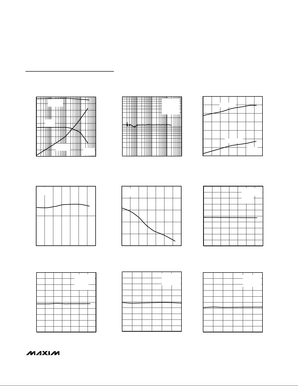
Typical Operating Characteristics
(TA = +25°C, unless otherwise noted.)
100n
10f
-40 -20 0 20 40 60 80 100 120
LEAKAGE CURRENT vs. TEMPERATURE
100f
MAX4539-01
TEMPERATURE (°C)
LEAKAGE CURRENT (A)
10p
1p
100p
10n
1n
V+ = 5V
V- = -5V
COM(OFF)
NO(OFF)
COM(ON)
0
10
20
30
50
60
40
70
80
90
100
0 1.0 1.5 2.00.5 2.5 3.0 3.5 4.54.0 5.0
ON-RESISTANCE vs. V
COM
AND TEMPERATURE
(SINGLE SUPPLY)
MAX4539-02
V
COM
(V)
R
ON
(Ω)
TA = +85°C
TA = +70°C
TA = +25°C
TA = -40°C
V+ = 5V
V- = 0
0
10
20
30
40
50
60
-5 -3 -2 -1-4 012 435
ON-RESISTANCE vs. V
COM
AND TEMPERATURE
(DUAL SUPPLIES)
MAX4539-03
V
COM
(V)
R
ON
(Ω)
TA = +85°C
TA = +70°C
TA = +25°C
TA = -40°C
V+ = 5V
V- = -5V
30
50
40
60
90
100
80
70
110
-5 -3 -2 -1 0-4 12345
ON-RESISTANCE vs. V
COM
(DUAL SUPPLIES)
MAX4539-04
V
COM
(V)
R
ON
(Ω)
V+ = 2.7V
V- = -2.7V
V+ = 3V
V- = -3V
V+ = 5V
V- = -5V
V+ = 2.4V
V- = -2.4V
0
40
20
60
140
160
120
100
80
180
234 5
ON/OFF TIME vs. SUPPLY VOLTAGE
MAX4539-07
V+, V- (V)
t
ON
, t
OFF
(ns)
tON
t
OFF
30
70
50
90
150
170
130
110
190
0 23451 678910
ON-RESISTANCE vs. V
COM
(SINGLE SUPPLY)
MAX4539-05
V
COM
(V)
R
ON
(Ω)
V+ = 2.7V
V+ = 3V
V+ = 5V
V+ = 7.5V
V+ = 10V
V- = 0
100n
0.1p
-40 -20 0 20 40 60 80 100 120 140
SUPPLY CURRENT vs. TEMPERATURE
10p
1p
MAX4539-06
TEMPERATURE (°C)
I+ I- (A)
100p
1n
10n
I-
I+
V+ = 5V
V- = -5V
-40
-20
0
60
80
40
20
100
-40
-20 0
20
40
60 80
100
ON/OFF TIME vs. TEMPERATURE
MAX4539-08
TEMPERATURE (°C)
t
ON
, t
OFF
(ns)
tON
V+ = 5V
V- = -5V
t
OFF
-2
4
2
0
6
8
10
-5 -1-2-4-3 012345
CHARGE INJECTION vs. V
COM
MAX4539-09
V
COM
(V)
Q (pC)
DUAL SUPPLIES
V+ = 5V, V- = -5V
SINGLE SUPPLY
V+ = 5V
Page 9
MAX4539/MAX4540
Low-Voltage, Single 8-to-1 and
Dual 4-to-1 Cal-Multiplexers
_______________________________________________________________________________________
9
Typical Operating Characteristics (continued)
(TA = +25°C, unless otherwise noted.)
14.90
14.98
14.96
14.94
14.92
15.06
15.04
15.02
15.00
15.10
15.08
2.0 3.52.5 3.0 4.0 4.5 5.0
OFFSET DIVIDER OUTPUT vs. REFHI
MAX4539-17
REFHI (V)
OUTPUT RATIO (LSB)
V
REFLO
= 0
V+ = 5V
V- = -5V or 0
FREQUENCY RESPONSE
0
-10
-20
-30
-40
-50
LOSS (dB)
-60
-70
-80
-90
INSERTION
LOSS
ON
PHASE
OFF
ISOLATION
0.1 10 1001 1000
FREQUENCY (MHz)
MAX4539-10
V+ = 5V
V- = -5V
(V+ / 2) DIVIDER OUTPUT
vs. TEMPERATURE
2050.0
V+ = +5V
V- = -5V
2049.5
OUTPUT RATIO (LSB)
2049.0
-40
-20 0
20
40
TEMPERATURE (°C)
60 80
180
140
100
-20
-60
-100
-140
-180
MAX4539-13a
100
R
vs. TEMPERATURE
OUT
(V+ / 2) R
OUT
(V+ - V-) R
-20 0
20
TEMPERATURE (°C)
GAIN DIVIDER OUTPUT
vs. TEMPERATURE
-20 0
20
TEMPERATURE (°C)
60
20
PHASE (DEGREES)
OUTPUT RATIO (LSB)
TOTAL HARMONIC DISTORTION
vs. FREQUENCY
0.1
0.01
THD (%)
0.001
10 1k 10k100 100k
FREQUENCY (Hz)
(V+ - V-) DIVIDER OUTPUT
vs. TEMPERATURE
2558.5
V+ = 5V
V- = -5V
2558.4
2558.3
2558.2
2558.1
2558.0
-40
-20 0
40
20
TEMPERATURE (°C)
V+ = 5V
V- = -5V
600Ω IN/OUT
= 5Vp-p
V
IN
60 80
MAX4539-11
MAX4539-13b
100
(V+ / 2 DIVIDER AND V+ - V- DIVIDER)
6030
5980
5930
5880
(Ω)
OUT
R
5830
5780
5730
5680
-40
4081.10
4081.08
4081.06
4081.04
4081.02
4081.00
4080.98
OUTPUT RATIO (LSB)
4080.96
4080.94
4080.92
4080.90
-40
MAX4539-12
OUT
V+ = 5V
V- = -5V
60 80
40
V
REFHI
V
REFLO
V+ = 5V
V- = -5V
60 80
40
= 4.096V
= 0
100
MAX4539-14
100
OFFSET DIVIDER OUTPUT
vs. TEMPERATURE
15.10
15.08
15.06
15.04
15.02
15.00
14.98
OUTPUT RATIO (LSB)
14.96
14.94
14.92
14.90
-40
-20 0
GAIN DIVIDER OUTPUT vs. REFHI
40
20
TEMPERATURE (°C)
V
REFHI
V
REFLO
V+ = 5V
V- = -5V
60 80
= 4.096V
= 0
100
MAX4539-15
OUTPUT RATIO (LSB)
4081.10
4081.08
4081.06
4081.04
4081.02
4081.00
4080.98
4080.96
4080.94
4080.92
4080.90
2.0 3.52.5 3.0 4.0 4.5 5.0
REFHI (V)
V
= 0
REFLO
V+ = 5V
V- = -5V or 0
MAX4539-16
Page 10

MAX4539/MAX4540
Low-Voltage, Single 8-to-1 and
Dual 4-to-1 Cal-Multiplexers
10 ______________________________________________________________________________________
Typical Operating Characteristics (continued)
(TA = +25°C, unless otherwise noted.)
Pin Descriptions
PIN
Positive Supply VoltageV+1
FUNCTIONNAME
GroundGND2
MAX4539 (Single 8-to-1 Cal-Mux)
Reference High Voltage InputREFHI4
Negative Supply VoltageV-3
Multiplexer OutputCOM6
Channel Input 2NO28
Channel Input 1NO17
Reference Low Voltage InputREFLO5
Channel Input 4NO410
Channel Input 6NO612
Channel Input 5NO511
Channel Input 8NO814
Address Bit 1A116
Address Bit 2A215
Channel Input 7NO713
Channel Input 3NO39
Calibration Control InputCAL18
Address Latch Control InputLATCH20
Multiplexer EnableEN19
Address Bit 0A017
MAX4540 (Dual 4-to-1 Cal-Mux)
GroundGND2
Reference High Voltage InputREFHI4
Negative Supply VoltageV-3
Multiplexer Output ACOMA6
Channel Input 2ANO2A8
Channel Input 1ANO1A7
Reference Low Voltage InputREFLO5
Channel Input 4ANO4A10
Channel Input 2BNO2B12
Channel Input 1BNO1B11
Channel Input 4BNO4B14
PIN
Address Bit 1A116
Positive Supply VoltageV+1
FUNCTIONNAME
Multiplexer Output BCOMB15
Channel Input 3BNO3B13
Channel Input 3ANO3A9
Calibration Control InputCAL18
Address Latch Control InputLATCH20
Multiplexer EnableEN19
Address Bit 0A017
190
210
200
230
220
250
240
260
R
OUT
vs. TEMPERATURE
(OFFSET DIVIDER AND GAIN DIVIDER)
MAX4539-18
TEMPERATURE (°C)
R
OUT
(Ω)
-40
-20 0 20
40
60 80
100
V+ = 5V
V- = -5V
V
REFHI
= 4.096V
V
REFLO
= 0
GAIN DIVIDER
OFFSET DIVIDER
2045
2049
2048
2047
2046
2053
2052
2051
2050
2055
2054
24356
(V+ / 2) DIVIDER OUTPUT
vs. SUPPLY VOLTAGE
MAX4539-19a
V+, V- (V)
OUTPUT RATIO (LSB)
2550
2555
2560
2565
13245
(V+ - V-) DIVIDER OUTPUT
vs. SUPPLY VOLTAGE
MAX4539-19b
V+, V- (V)
OUTPUT RATIO (LSB)
Page 11

MAX4539/MAX4540
Low-Voltage, Single 8-to-1 and
Dual 4-to-1 Cal-Multiplexers
______________________________________________________________________________________ 11
Truth Tables
MAX4539 (Single 8-to-1 Cal-Mux)
State is latched when LATCH is high.X
NO20
NO10
NO40
NO60
NO50
NO30
NO80
REFHI1
(V+ / 2) Divider Mode, V
COM
= 2048/4096 V+1
(V+ - V-) Divider Mode , V
COM
= 2560/4096 (V+ - V-)1
CAL
Gain Divider Mode, V
COM
= 4081/4096 (V
REFHI
- V
REFLO
)1
All switches and dividers open. COM is high-Z. Latch contents set
to all 1’s.
X
COM
GND1
REFLO1
NO70
All switches and dividers open. COM is high-Z.1
Offset Divider Mode, V
COM
= 15/4096 (V
REFHI
- V
REFLO
)1
X
0
0
0
1
1
0
1
0
0
0
A2
1
X
1
0
1
1
1
X
0
0
1
0
0
1
1
0
0
1
A1
0
X
0
1
1
1
1
X
1
0
1
1
0
0
1
1
0
1
A0
1
X
0
0
0
1
0
1
1
1
1
1
1
1
1
1
1
1
EN
1
0
1
1
1
1
1
1
0
0
0
0
0
0
0
0
0
0
LATCH
0
X
0
0
0
0
0
MAX4540 (Dual 4-to-1 Cal-Mux)
State is latchedX
NO2A0
NO1A0
NO4A0
Gain Divider Mode1
GND1
NO3A0
All switches and dividers open.
COMA is high-Z.
1
CAL
All switches and dividers open.
COMA is high-Z.
COMA
X
Offset Divider Mode1
X
0
0
1
0
0
1
1
A1
X
1
X
1
0
1
1
0
0
1
A0
X
0
1
1
1
1
1
1
1
1
EN
0
1
1
0
0
0
0
0
0
0
LATCH
X
0
State is latched
NO2B
NO1B
NO4B
REFLO
GND
NO3B
All switches and dividers open.
COMB is high-Z.
All switches and dividers open.
COMB is high-Z.
COMB
REFLO
X = Don’t care
X = Don’t care
Page 12

MAX4539/MAX4540
Low-Voltage, Single 8-to-1 and
Dual 4-to-1 Cal-Multiplexers
12 ______________________________________________________________________________________
Detailed Description
The MAX4539/MAX4540 are multiplexers with additional calibration features. Internal resistor-dividers generate accurate voltage ratios from an external voltage
reference, allowing zero- and full-scale calibration of
ADC systems as well as facilitation of system self-monitoring. To access the resistor-dividers, assert the CAL
pin. When CAL and ENABLE are asserted, the three
address pins select one of the various resistor-divider
or external reference outputs. The MAX4539/MAX4540
also contain a LATCH input that allows the state of the
CAL and address signals to be captured.
Calibration Functions
The Gain Divider, Offset Divider, REFHI and REFLO
modes allow calibration of offset and gain errors in
ADC systems. The Gain Divider mode outputs a voltage ratio that is 4081/4096 of V
REFHI
- V
REFLO
, accurate to 0.1/4096, or better than 15 bits. The Offset
Divider mode outputs a voltage ratio that is 15/4096 of
V
REFHI
- V
REFLO
, also accurate to 0.1/4096. The REFHI
mode allows the voltage on the REFHI pin to be
switched to the output. The REFLO mode allows the
voltage on the REFLO pin to be switched to the output.
Self-Monitoring Functions
The self-monitoring functions are intended to allow an
ADC to measure its own supply voltage. The MAX4539
has an internal divide-by-two resistor string between V+
and GND that is accurate to 8 bits (16/4096). It also has
a 5/8 resistor string between V+ and V- that is also
accurate to 8 bits. This divider string allows measurement of the negative supply with a unipolar ADC. GND
can also be switched to the output, eliminating the
need for an additional multiplexer channel.
Applications Information
The MAX4539/MAX4540’s construction is typical of most
CMOS analog switches. There are three supply pins:
V+, V-, and GND. The positive and negative power supplies provide drive to the internal CMOS switches and
set the limits of the analog voltage on any switch.
Reverse-biased ESD protection diodes are internally
connected between each analog signal pin and both V+
and V-. If the voltage on any pin exceeds V+ or V-, one
of these diodes will conduct. During normal operation,
these reverse-biased ESD diodes leak, forming the only
current drawn from V-.
Virtually all the analog-leakage current is through the
ESD diodes. Although the ESD diodes on a given signal pin are identical, and therefore fairly well balanced, they are reverse-biased differently. Each is
biased by either V+ or V- and the analog signal. This
means their leakage varies as the signal varies. The
difference in the two-diode leakage from the signal
path to the V+ and V- pins constitutes the analogsignal path leakage current. All analog-leakage current flows to the supply terminals, not to the other
switch terminal, which explains how both sides of a
given switch can show leakage currents of either the
same or opposite polarity.
There is no connection between the analog-signal
paths and GND. The analog-signal paths consist of an
N-channel and P-channel MOSFET with their sources
and drains paralleled and their gates driven out of
phase with V+ and V- by the logic-level translators.
V+ and GND power the internal logic and logic-level
translators and set the input-logic thresholds. The logiclevel translators convert the logic levels to switched V+
and V- signals to drive the gates of the analog switches.
This drive signal is the only connection between the
logic supplies and the analog supplies. All pins have
ESD protection to V+ and to V-.
Increasing V- has no effect on the logic-level thresholds, but it does increase the drive to the P-channel
switches, which reduces their on-resistance. V- also
sets the negative limit of the analog-signal voltage.
The logic-level thresholds are CMOS- and TTL- compatible when V+ is +5V. As V+ is raised, the threshold
increases slightly; when V+ reaches +12V, the level
threshold is about 3.2V. Although that is above the TTL
output high-level minimum of 2.4V, it is still compatible
with CMOS outputs.
Bipolar-Supply Operation
The MAX4539/MAX4540 operate with bipolar supplies
between ±2.7V and ±6V. The V+ and V- supplies need
not be symmetrical, but their sum cannot exceed the
absolute maximum rating of 13V.
Note: Do not connect the MAX4539/MAX4540 V+ pin
to +3V AND connect the logic-level input pins to TTL
logic-level signals. TTL logic-level outputs can
exceed the absolute maximum ratings, which will
cause damage to the part and/or external circuits.
Caution: The absolute maximum V+ to V- differential
voltage is 13V. Typical “±6-Volt” or “12-Volt” supplies with ±10% tolerances can be as high as 13.2V.
This voltage can damage the MAX4539/MAX4540.
Even ±5% tolerance supplies may have overshoot
or noise spikes that exceed 13V.
Page 13
MAX4539/MAX4540
Low-Voltage, Single 8-to-1 and
Dual 4-to-1 Cal-Multiplexers
______________________________________________________________________________________ 13
Single-Supply Operation
The MAX4539/MAX4540 operate from a single supply
between +2.7V and +12V when V- is connected to
GND. All of the bipolar precautions must be observed.
However, these parts are optimized for ±5V operation,
and most AC and DC characteristics are degraded significantly when departing from ±5V. As the overall supply voltage (V+ to V-) is lowered, switching speed,
on-resistance, off isolation, and distortion will degrade.
(see the
Typical Operating Characteristics
section).
Single-supply operation also limits signal levels and
interferes with ground referenced signals. When V- = 0,
AC signals are limited to -0.3V. Voltages below -0.3V can
be clipped by the internal ESD-protection diodes, and
the parts can be damaged if excessive current flows.
Power Up
During power up, on-chip latches will strobe whatever
addresses are present if EN goes high before LATCH
reaches a logic high. When this condition occurs, one of
the internal dividers connected between the supplies
may inadvertently turn on, causing higher supply current
(~200µA supply current) when the enable input is toggled. Avoid this condition by ensuring that EN pin stays
low until the remaining logic inputs are valid. To accomplish this, connect a resistor from EN to ground or apply
a low voltage to EN before the other logic inputs go high.
Power Off
When power to the MAX4539/MAX4540 is off (i.e., V+ =
V- = 0), the Absolute Maximum Ratings still apply. This
means that neither logic-level inputs on NO_ nor signals on COM_ can exceed ±0.3V. Voltages beyond
±0.3V cause the internal ESD-protection diodes to conduct, and the parts can be damaged if excessive current flows.
Chip Information
TRANSISTOR COUNT: 561
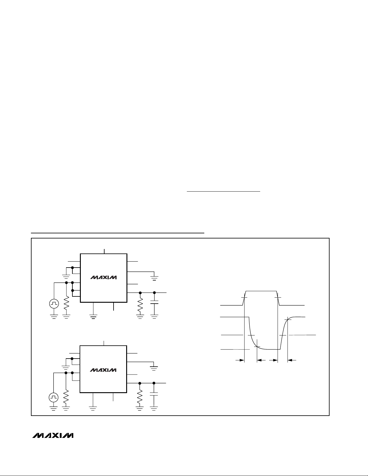
Test Circuits/Timing Diagrams
Figure 1. Transition Time
+5V
V+
NO2–NO7
V-
-5V
V+
NO2B–NO3B
NO1A–NO2A
COMB
V-
-5V
NO1
NO8
COM
NO1B
NO4B
300Ω
300Ω
+3V
-3V
V
35pF
+3V
-3V
V
35pF
50Ω
50Ω
EN
LATCH
CAL
A0
A1
A2
EN
LATCH
CAL
A0
A1
MAX4539
GND
+5V
MAX4540
GND
V+
V+
LOGIC
COM
SWITCH
OUTPUT
COM
INPUT
V
EN
V
NO1
V
COM
V
NO8
V+
0V
, V
NO1B
0V
, V
NO4B
50%
t
TRANS
90%
t
TRANS
50%
t
< 20ns
R
< 20ns
t
F
90%
Page 14

MAX4539/MAX4540
Low-Voltage, Single 8-to-1 and
Dual 4-to-1 Cal-Multiplexers
14 ______________________________________________________________________________________
Test Circuits/Timing Diagrams (continued)
Figure 2. Break-Before-Make Interval
Figure 3. Enable Switching Time
+5V
MAX4539
GND
MAX4540
GND
V+
NO1–NO8
-5V
+5V
V+
NO1A–NO4B
NO1B–NO4B
-5V
V-
V-
COM
COMA
300Ω
300Ω
+3V
+3V
35pF
35pF
V
COM
V
COM
V+
V
A
V+
V
A
EN
LATCH
CAL
A0
A1
A2
50Ω
EN
LATCH
CAL
A0
A1
50Ω
LOGIC
INPUT
V
A
SWITCH
OUTPUT
V
COM
LOGIC
INPUT
V
A
SWITCH
OUTPUT
V
COM
0.8V
0.8V
NO_
NO_
V+
0V
0V
V+
0V
90% 90%
0V
50% 50%
90%
t
OPEN
t
50%
OPEN
50%
tR < 20ns
tF < 20ns
tR < 20ns
tF < 20ns
+5V
V+
MAX4539
GND
+5V
V+
MAX4540
GND
50Ω
50Ω
V
EN
EN
LATCH
CAL
A0
A1
A2
V
EN
EN
LATCH
CAL
A0
A1
NO1
NO2–NO8
COM
V-
-5V
NO1B
NO2B–NO4B
NO1A–NO4A
COMB
V-
-5V
300Ω
300Ω
+3V
+3V
35pF
35pF
50%
tR < 20ns
tF < 20ns
t
OFF
NO1
V+
0V
, V
)
NO1B
0V
t
ON
50%
90%90%
V
EN
V
COM
0.8(V
V
COM
V
COM
Page 15

MAX4539/MAX4540
Low-Voltage, Single 8-to-1 and
Dual 4-to-1 Cal-Multiplexers
______________________________________________________________________________________ 15
Figure 4. Charge Injection
Test Circuits/Timing Diagrams (continued)
Figure 5. Off-Isolation/Crosstalk
MAX4539
GND
MAX4540
GND
+5V
+5V
V+
COM
V-
-5V
V+
COMA
V-
-5V
V
COM
CL = 1nF
V
COM
CL = 1nF
_
LOGIC
INPUT
V
EN
V
COM
LOGIC
INPUT
V
EN
V
COM
V+
0V
IS THE MEASURED VOLTAGE DUE TO CHARGE TRANSFER
∆V
OUT
ERROR Q WHEN THE CHANNEL TURNS OFF.
Q = ∆V
OUT x CL
V+
0V
∆V
IS THE MEASURED VOLTAGE DUE TO CHARGE TRANSFER
OUT
ERROR Q WHEN THE CHANNEL TURNS OFF.
Q = ∆V
OUT x CL
OFFON ON
OFFON ON
∆V
OUT
∆V
OUT
R
S
NO_
EN
V
S
V
S
CHANNEL
SELECT
R
S
CHANNEL
SELECT
A0
A1
A2
CAL
LATCH
NO_
EN
A0
A1
CAL
LATCH
V+
EN
MAX4539
V+
MAX4540
A
+5V
10nF
NETWORK
V+
NO_
COM_
GND
CALLATCH
V-
10nF
+5V
V
V
COM
ANALYZER
IN
50Ω
MEAS. REF
50Ω 50Ω
MEASUREMENTS ARE STANDARDIZED AGAINST SHORT AT SOCKET TERMINALS.
NOTES:
OFF-ISOLATION IS MEASURED BETWEEN COM AND “OFF” TERMINAL ON EACH SWITCH.
ON LOSS IS MEASURED BETWEEN COM AND “ON” TERMINAL ON EACH SWITCH.
50Ω
OFF ISOLATION = 20log
CROSSTALK = 20log
V
OUT
V
IN
V
OUT
V
IN
Page 16

MAX4539/MAX4540
Low-Voltage, Single 8-to-1 and
Dual 4-to-1 Cal-Multiplexers
16 ______________________________________________________________________________________
Figure 6. NO_/COM_ Capacitance
Test Circuits/Timing Diagrams (continued)
Figure 7. Setup Time, Hold Time, Latch Pulse Width
Figure 8. Enable Setup Time
+5V
+5V
CAL,
GND
V+
MAX4539
LATCH,
EN
-5V
NO1
NO8
COM
V-
CAPACITANCE
CHANNEL
SELECT
A2
A1
A0
V+
+3V
EN
NO2
NO1, NO3-NO8
A1
A2
CAL
MAX4539
GND
V+
LATCH
A0
COM
V-
1MHz
ANALYZER
f = 1MHz
CHANNEL
SELECT
LATCH
V+
NO1A
A1
MAX4540
A0
CAL,
LATCH,
GND
EN
EN
50%
NO4A
COMA
V-
-5V
50%
t
1MHz
CAPACITANCE
ANALYZER
f = 1MHz
50%
ES
LATCH
ADDRESS (A_)
V-
t
MPW
V
V
50%50%
t
H
t
S
IH
IL
Page 17

MAX4539/MAX4540
Low-Voltage, Single 8-to-1 and
Dual 4-to-1 Cal-Multiplexers
______________________________________________________________________________________ 17
Pin Configurations/Functional Diagrams (continued)
V+
GND
REFHI
REFLO
COMA
NO1A
NO2A
NO3A
NO4A
1
2
V-
3
4
4081R
5
6
7
8
9
10
MAX4540
15R
LOGIC
DECODER
4081R
15R
20
LATCH
19
EN
18
CAL
17
A0
16
A1
15
COMB
14
NO4B
13
NO3B
12
NO2B
11
NO1B
Page 18

MAX4539/MAX4540
Low-Voltage, Single 8-to-1 and
Dual 4-to-1 Cal-Multiplexers
18 ______________________________________________________________________________________
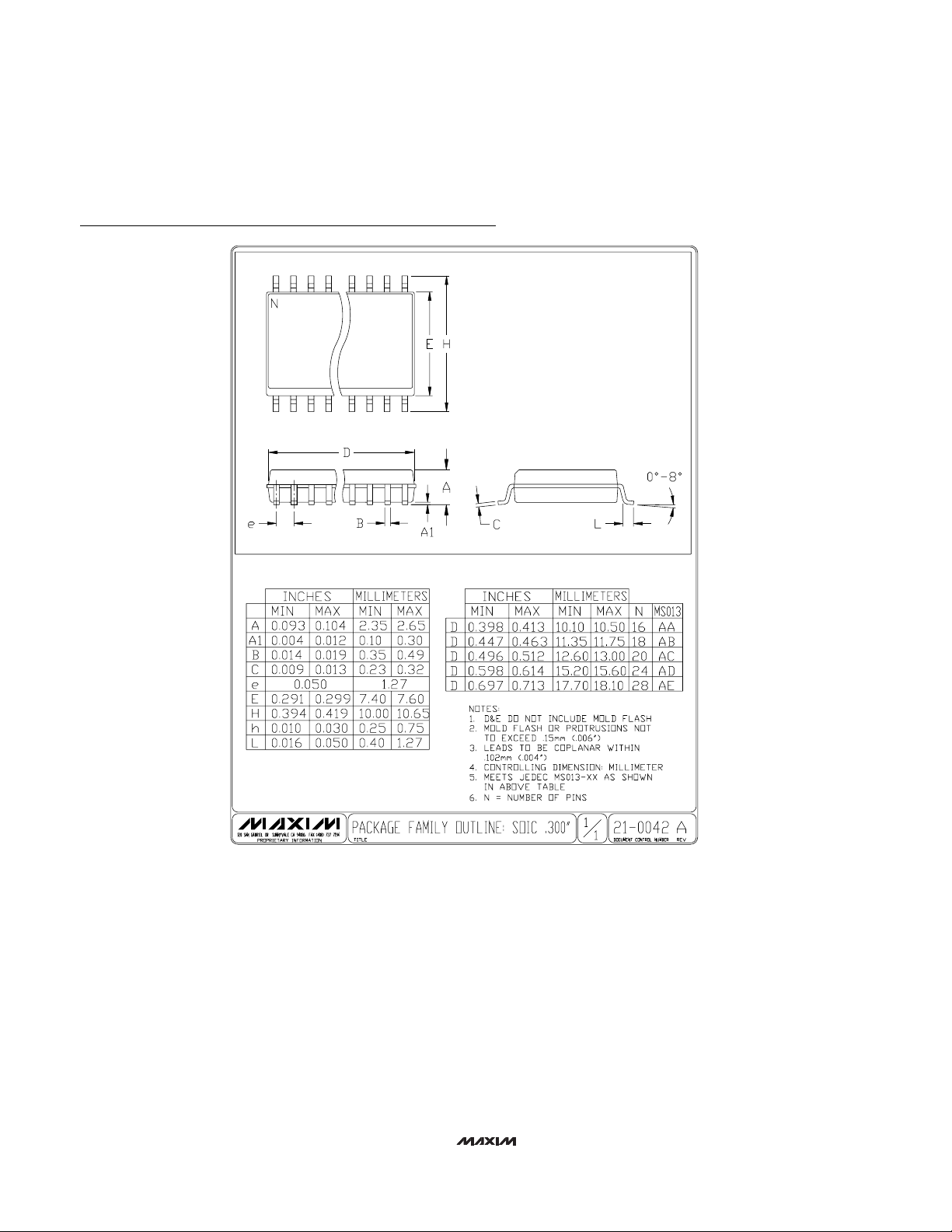
Package Information
SSOP.EPS
Page 19

MAX4539/MAX4540
Low-Voltage, Single 8-to-1 and
Dual 4-to-1 Cal-Multiplexers
______________________________________________________________________________________ 19
Package Information (continued)
PDIPN.EPS
Page 20
MAX4539/MAX4540
Low-Voltage, Single 8-to-1 and
Dual 4-to-1 Cal-Multiplexers
Maxim cannot assume responsibility for use of any circuitry other than circuitry entirely embodied in a Maxim product. No circuit patent licenses are
implied. Maxim reserves the right to change the circuitry and specifications without notice at any time.
20
____________________Maxim Integrated Products, 120 San Gabriel Drive, Sunnyvale, CA 94086 408-737-7600
© 1999 Maxim Integrated Products Printed USA is a registered trademark of Maxim Integrated Products.
Package Information (continued)
SOICW.EPS
Page 21
WWW.ALLDATASHEET.COM
Copyright © Each Manufacturing Company.
All Datasheets cannot be modified without permission.
This datasheet has been download from :
www.AllDataSheet.com
100% Free DataSheet Search Site.
Free Download.
No Register.
Fast Search System.
www.AllDataSheet.com
 Loading...