

Page 1
General Description
The MAX4534 (single 4-to-1) and MAX4535 (dual 2-to-
1) fault-protected multiplexers operate with ±4.5V to
±20V dual supplies or a +9V to +36V single supply.
These multiplexers feature fault-protected inputs, railto-rail signal-handling capability, and overvoltage
clamping at 150mV beyond the rails. Both parts feature
±40V overvoltage protection with supplies off and ±25V
protection with supplies on. On-resistance is 400Ω max
and is matched between channels to 10Ω max. All digital inputs have TTL logic thresholds, ensuring
TTL/CMOS-logic compatibility when using a single
+12V or dual ±15V supplies.
Applications
Data-Acquisition Systems
Industrial and Process Control
Avionics
Signal Routing
Redundant/Backup Systems
Features
♦ ±40V Fault Protection with Power Off
±25V Fault Protection with ±15V Supplies
♦ No Power-Supply Sequencing Required
♦ All Channels Off with Power Off
♦ Rail-to-Rail Signal Handling
♦ Output Clamped to Appropriate Supply Voltage
During Fault Condition
♦ 1.0kΩ typ Output Clamp Resistance During
Overvoltage
♦ 400Ω max On-Resistance
♦ 20ns typ Fault Response Time
♦ ±4.5V to ±20V Dual Supplies
+9V to +36V Single Supply
♦ TTL/CMOS-Compatible Logic Inputs
MAX4534/MAX4535
Fault-Protected, High-Voltage,
Single 4-to-1/Dual 2-to-1 Multiplexers
________________________________________________________________ Maxim Integrated Products 1
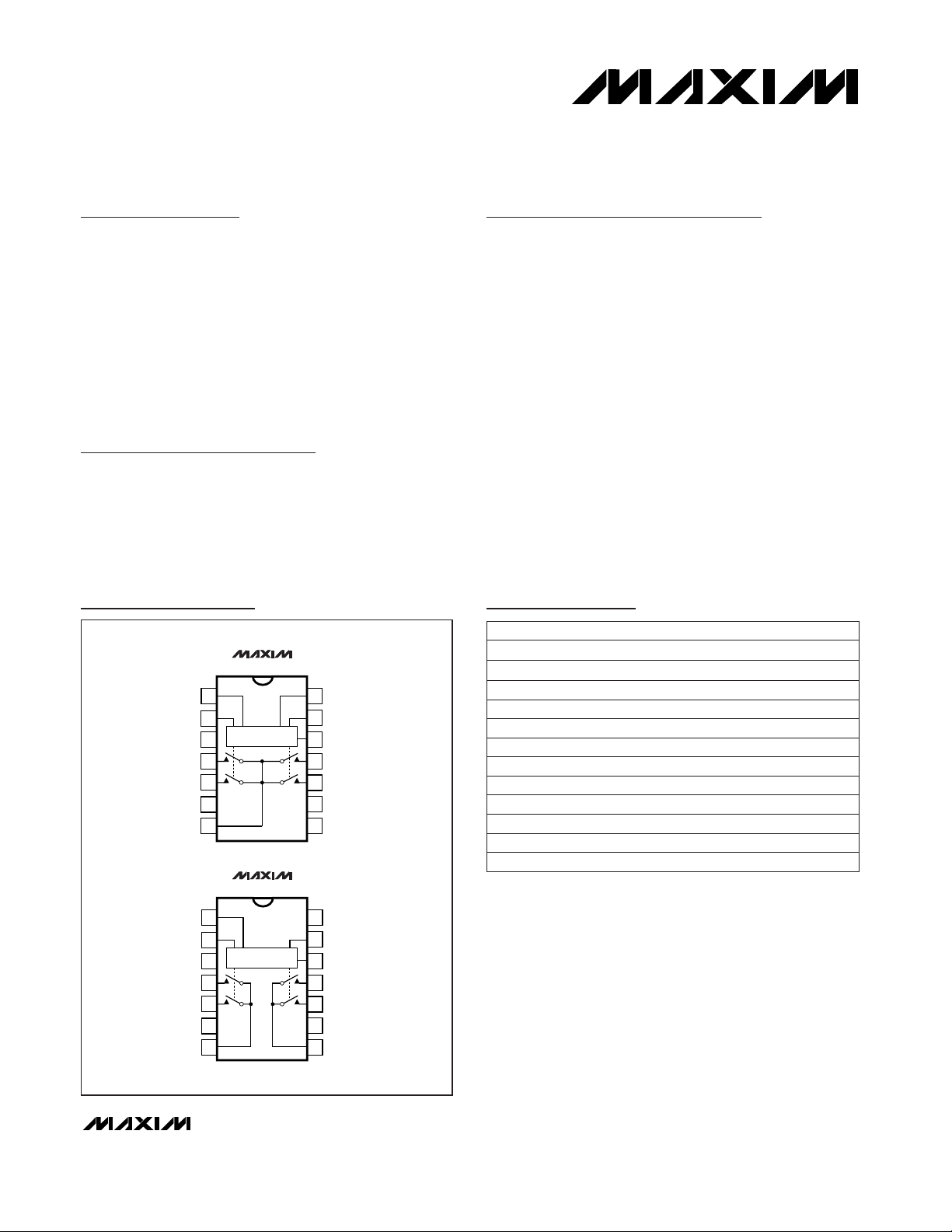
14
13
12
11
10
9
8
1
2
3
4
5
6
7
A1
GND
V+
NO3
NO1
V-
EN
A0
TOP VIEW
MAX4534
NO4
N.C.
N.C.
COM
N.C.
NO2
TSSOP/SO/DIP
LOGIC
14
13
12
11
10
9
8
1
2
3
4
5
6
7
N.C.
GND
V+
NO1B
NO1A
V-
EN
A0
MAX4535
NO2B
N.C.
COMB
COMA
N.C.
NO2A
TSSOP/SO/DIP
LOGIC
19-1609; Rev 2; 5/05
Ordering Information
Pin Configurations
14 Narrow SO0°C to +70°CMAX4535CSD
14 TSSOP0°C to +70°C
MAX4535CUD
14 Plastic DIP-40°C to +85°CMAX4534EPD
14 Narrow SO-40°C to +85°CMAX4534ESD
14 TSSOP-40°C to +85°CMAX4534EUD
14 Plastic DIP
14 Narrow SO
14 TSSOP
PIN-PACKAGETEMP RANGE
0°C to +70°C
0°C to +70°C
0°C to +70°CMAX4534CPD
MAX4534CSD
MAX4534CUD
PART
14 Plastic DIP-40°C to +85°CMAX4535EPD
14 Narrow SO-40°C to +85°CMAX4535ESD
14 TSSOP-40°C to +85°CMAX4535EUD
14 Plastic SO0°C to +70°CMAX4535CPD
For pricing, delivery, and ordering information, please contact Maxim/Dallas Direct! at
1-888-629-4642, or visit Maxim’s website at www.maxim-ic.com.
Page 2
MAX4534/MAX4535
Fault-Protected, High-Voltage,
Single 4-to-1/Dual 2-to-1 Multiplexers
2 _______________________________________________________________________________________
ABSOLUTE MAXIMUM RATINGS
ELECTRICAL CHARACTERISTICS—Dual Supplies
(V+ = +15V, V- = -15V, V
A_H
= V
ENH
= 2.4V, V
A_L
= V
E
NL
= 0.8V, TA= T
MIN
to T
MAX
, unless otherwise noted. Typical values are at
T
A
= +25°C.) (Note 3)
Stresses beyond those listed under “Absolute Maximum Ratings” may cause permanent damage to the device. These are stress ratings only, and functional
operation of the device at these or any other conditions beyond those indicated in the operational sections of the specifications is not implied. Exposure to
absolute maximum rating conditions for extended periods may affect device reliability.
(Voltages Referenced to GND)
V+ ...........................................................................-0.3V to +44V
V- ............................................................................-44V to +0.3V
V+ to V-...................................................................-0.3V to +44V
COM_, A_, EN (Note 1)........................ (V- - 0.3V) to (V+ + 0.3V)
NO_ (Note 2)...........................................(V+ - 40V) to (V- + 40V)
NO_ to COM_ (Note 2) ............................................-40V to +40V
NO_ Overvoltage with Switch Power On (Note 2). ..-36V to +36V
NO_ Overvoltage with Switch Power Off (Note 2). ..-40V to +40V
Continuous Current into Any Terminal..............................±30mA
Peak Current Into Any Terminal
(pulsed at 1ms, 10% duty cycle).................................±100mA
Continuous Power Dissipation (T
A
= +70°C)
14-Pin TSSOP (derate 6.3mW/°C above +70°C) ..........500mW
14-Pin Narrow SO (derate 8mW/°C above +70°C) .......640mW
14-Pin Plastic DIP (derate 10mW/°C above +70°C) .....800mW
Operating Temperature Ranges
MAX453_C_D.......................................................0°C to +70°C
MAX453_E_D....................................................-40°C to +85°C
Storage Temperature Range .............................-65°C to +150°C
Lead Temperature (soldering, 10s) .................................+300°C
Note 1: COM_, EN, and A_ pins are not fault protected. Signals on COM_, EN, or A_ exceeding V+ or V- are clamped by internal
diodes. Limit forward diode current to maximum current rating.
Note 2: NO_ pins are fault-protected. Signals on NO_ exceeding -25V to +25V may damage the device during power-on conditions.
When the power is off the maximum voltage range is -40V to +40V.
T
A
C, E
+25°C
+25°C
C, E
+25°C
C, E
+25°C
C, E
C, E
+25°C
C, E
+25°C
+25°C
C, E
CONDITIONS
V
COM_
= ±10V,
V
NO_
= –+10V
V
COM_
= ±10V, I
NO_
= 1mA
V
COM_
= ±10V, I
NO_
= 1mA
V
NO_
= ±10V, V
COM_
= –+10V
Applies with power on or off
PARAMETER SYMBOL MIN TYP MAX UNITS
15
On-Resistance Match Between
Channels (Note 4)
∆R
ON
210
Ω
On-Resistance Ω
500
-0.5 0.01 0.5
nA
-5 5
NO_ Off-Leakage Current
(Note 5)
I
NO_(OFF)
Fault-Free Analog Signal Range V
NO_
V- V+
V
R
ON
275 400
I
COM_(OFF)
nA
-2 0.05 2
-60 60
-1 0.05 1
-30 30
COM_ Off-Leakage Current
(Note 5)
I
COM_(ON)
nA
V
NO_
-2 0.1 2
Applies with power on
+25°C
-80 80
C, E
COM_ On-Leakage Current
(Note 5)
-1 0.1 1
-40 40
-25 +25
-40 +40
Fault-Protected Analog Signal
Range (Note 6)
V
Applies with power off
I
COM_
nA-20 20
-1 1
COM_ Output Leakage Current,
Supplies On
V
COM_
= ±10V,
V
NO_
= floating
MAX4535
MAX4535
V
NO_
= ±25V, VEN= 0, V
COM_
= 0
MAX4534
MAX4534
FAULT PROTECTION
ANALOG SWITCH
µA
Page 3
MAX4534/MAX4535
Fault-Protected, High-Voltage,
Single 4-to-1/Dual 2-to-1 Multiplexers
_______________________________________________________________________________________ 3
ELECTRICAL CHARACTERISTICS—Dual Supplies (continued)
(V+ = +15V, V- = -15V, V
A_H
= V
ENH
= 2.4V, V
A_L
= V
E
NL
= 0.8V, TA= T
MIN
to T
MAX
, unless otherwise noted. Typical values are at
T
A
= +25°C.) (Note 3)
V
NO_
= ±25VR
COM_
ns
ns
Enable Turn-On Time
Transition Time
500
130 350
t
TRANS
Figure 2
C, E
+25°C
10 60
V
NO_
= ±10V, RL = 1kΩ,
Figure 4
nst
BBM
Break-Before-Make Time Delay
UNITSMIN TYP MAXSYMBOLPARAMETER CONDITIONS TA
400
135 275
t
ON
µA-1 1IA_, I
EN
Input Logic Current
V0.8
V
A_L,
V
ENL
Input Logic Voltage Low
V2.4
V
A_H,
V
ENH
Input Logic Voltage High
µs2.5± Fault Recovery Time
ns20± Fault Response Time
COM_ On Clamp Output
Resistance, Supplies On
kΩ
0.1 1.0 2.5
COM_ On Clamp Output
Current, Supplies On
-13 -11 -7
mA
71013
I
COM_
µA
nA
-5 5
-20 20
I
NO_
NO_ Input Leakage Current,
Supplies Off
I
NO_
NO_ Input Leakage Current,
Supplies On
nA
-20 20
-200 200
V
NO_
= ±10V, RL= 1kΩ,
Figure 3
V
A_
= VEN= 0.8V or 2.4V
RL= 10kΩ, V
NO_
= ±25V
RL = 10kΩ, V
NO_
= ±25V
V
NO_
= ±40V, V
COM_
= 0,
V+ = 0, V- = 0
V
NO_
= ±25V, V
COM_
= –+10V,
V
EN
= 0
C, E
+25°C
C, E
+25°C
+25°C
+25°C
C, E
+25°C
110
CL= 1nF, V
NO_
= 0, RS= 0,
Figure 5
pCQ
Charge Injection
(Note 7)
-62
RL= 50Ω, V
NO_
= 1V
RMS
,
f = 1MHz, Figure 6
dBV
ISO
Off-Isolation
(Note 8)
V
NO_
= +25V V
COM_
= 0
0.08 3C, E
mVV- - 400 V+ + 400Fault Trip Threshold RL= 1kΩ
5f = 1MHz, Figure 8 pFC
NO_(OFF)
-53
NO_ Off-Capacitance
RL= 50Ω, V
NO_
= 1V
RMS
,
f = 1MHz, Figure 7
dB
6.5
V
CT
f = 1MHz,
Figure 8
Channel-to-Channel Crosstalk
(Note 9)
pFC
COM_(OFF)
COM_ Off-Capacitance
MAX4534
4
13.5
f = 1MHz,
Figure 8
pFC
COM_(ON)
COM_ On-Capacitance
MAX4534
10.5
V
NO_
= -25V V
COM_
= 0
MAX4535
MAX4535
nsEnable Turn-Off Time
250
60 200
t
OFF
V
NO_
= ±10V, RL = 1kΩ,
Figure 3
C, E
+25°C
SWITCH DYNAMIC CHARACTERISTICS
LOGIC INPUT
Page 4
MAX4534/MAX4535
Fault-Protected, High-Voltage,
Single 4-to-1/Dual 2-to-1 Multiplexers
4 _______________________________________________________________________________________
UNITSMIN TYP MAXSYMBOLPARAMETER CONDITIONS T
A
10
0.01 1
I
GND
GND Supply Current
µA
225 400
I+V+ Supply Current
±4.5 ±20
All V
A_
= VEN= 0 or 15V
All V
A_
= VEN= 0 or 5V
C, E
+25°C
+25°C
Power-Supply Range V+, V- V
600C, E
300C, E
µA
125 200
All V
A_
= VEN= 0, 5V, or 15V
+25°C
V
0V+
V
NO_
Fault-Free Analog Signal Range
I
NO_(OFF)
NO_ Off-Leakage Current
(Notes 5, 10)
-10 10
nA
-0.5 0.01 0.5
Ω
10 25
∆R
ON
On-Resistance Match Between
Channels (Note 5)
40
UNITSMIN TYP MAXSYMBOLPARAMETER
Applies with power on or off
V
COM_
= 10V, 1V;
V
NO_
= 1V, 10V
V
COM_
= 10V, I
NO_
= 500µA
CONDITIONS
C, E
+25°C
+25°C
C, E
T
A
650 950
R
ON
1100
ΩOn-Resistance V
COM_
= 10V, I
NO_
= 500µA
+25°C
C, E
ELECTRICAL CHARACTERISTICS—Dual Supplies (continued)
(V+ = +15V, V- = -15V, V
A_H
= V
ENH
= 2.4V, V
A_L
= V
E
NL
= 0.8V, TA= T
MIN
to T
MAX
, unless otherwise noted. Typical values are at
T
A
= +25°C.) (Note 3)
ELECTRICAL CHARACTERISTICS—Single +12V Supply
(V+ = +12V, V- = 0, V
A_H
= V
ENH
= 2.4V, V
A_L
= V
ENL
= 0.8V, TA= T
MIN
to T
MIN
, unless otherwise noted. Typical values are at
T
A
= +25°C.) (Note 3)
300
100 200
All V
A_
= VEN= 5V
C, E
+25°C
I
COM_(OFF)
COM_ Off-Leakage Current
(Notes 5, 10)
-60 60
nA
-22
V
COM_
= 10V,
1V;
V
NO_
= 1V,10V
C, E
+25°C
-30 30
-
11
C, E
+25°C
I
COM_(ON)
COM_ On-Leakage Current
(Notes 5, 10)
-80 80
nA
-22
V
COM_
= 10V,
1V;
V
NO_
= 10V,
1V, or floating
C, E
+25°C
-40 40
-11
C, E
+25°C
MAX4534
MAX4534
MAX4535
MAX4535
300C, E
125 200
I-V- Supply Current
All V
A_
= VEN= 0 or 15V
+25°C
POWER SUPPLY
µA
Page 5
MAX4534/MAX4535
Fault-Protected, High-Voltage,
Single 4-to-1/Dual 2-to-1 Multiplexers
_______________________________________________________________________________________ 5
ELECTRICAL CHARACTERISTICS—Single +12V Supply (continued)
(V+ = +12V, V- = 0, V
A_H
= V
ENH
= 2.4V, V
A_L
= V
ENL
= 0.8V, TA= T
MIN
to T
MIN
, unless otherwise noted. Typical values are at
T
A
= +25°C.) (Note 3)
210+25°C
CL= 1nF, V
NO_
= 0, RS= 0,
Figure 5
pC
ns
Enable Turn-On Time
100 250+25°C
V
COM_
= 10V, RL = 2kΩ,
Figure 3
nst
OFF
Enable Turn-Off Time
350
Q
C, E
50 100+25°C
Charge Injection (Note 7)
V
COM_
= 10V, RL = 2kΩ,
Figure 4
ns
-62
t
BBM
RL= 50Ω, V
NO_
= 1V
RMS,
f = 1MHz, Figure 6
Break-Before-Make Time Delay
dBV
ISO
Off-Isolation (Note 8)
700
220 500
t
ON
V
COM_
= 10V, RL = 2kΩ,
Figure 3
C, E
+25°C
dB-65V
CT
Channel-to-Channel Crosstalk
(Note 9)
RL= 50Ω, V
NO_
= 1V
RMS,
f = 1MHz, Figure 7
V
NO_
= 25VR
COM_
UNITSMIN TYP MAXSYMBOLPARAMETER CONDITIONS T
A
µA-1 1IA_, I
EN
Input Logic Current
V0.8
V
A_L,
V
ENL
Input Logic Voltage Low
V2.4
V
A_H,
V
ENH
Input Logic Voltage High
mVV- - 400 V+ + 400Fault Trip Threshold
COM_ ON Output Resistance,
Supply On
kΩ2.4 6
COM_ ON Output Current,
Supply On
nA235I
COM_
-20 20
V
-25 25
V
NO_
Fault-Protected Analog Signal
Range (Note 6)
µA-5 5
-20 0.1 20
I
NO_
NO_ Input Leakage Current,
Supply Off
I
NO_
NO_ Input Leakage Current,
Supply On
-1 1
I
COM_
COM_ Output Leakage Current,
Supply On
-20 20
-5 5
V
A_
= VEN= 0.8V or 2.4V
Applies with all power on
RL= 1kΩ
V
NO_
= ±40V, V+ = 0
V
NO_
= ±25V, V
COM_
= 0,
V
NO_
= ±25V,
V
COM
= 0
V
NO_
= 25V
+25°C
+25°C
C, E
+25°C
+25°C
C, E
+25°C
C, E
+25°C
µA
Applies with all power off -40 40
nA
µA
nA
nA
FAULT PROTECTION
LOGIC INPUT
SWITCH DYNAMIC CHARACTERISTICS
ANALOG SWITCH
Page 6

µA
MAX4534/MAX4535
Fault-Protected, High-Voltage,
Single 4-to-1/Dual 2-to-1 Multiplexers
6 _______________________________________________________________________________________
Typical Operating Characteristics
(V+ = +15V, V- = -15V, TA= +25°C, unless otherwise noted.)
0
200
100
400
300
600
500
700
900
800
1000
-20 -10 -5-15 0 5 10 15 20
ON-RESISTANCE vs.
V
COM
(DUAL SUPPLIES)
MAX4534 toc01
V
COM
(V)
R
ON
(Ω)
V+ = +15V
V- = -15V
V+ = +10V
V- = -10V
V+ = +20V
V- = -20V
V+ = +4.5V
V- = -4.5V
0
200
100
400
300
600
500
700
900
800
1100
1000
0101552025303540
ON-RESISTANCE vs.
V
COM
(SINGLE SUPPLY)
MAX4534 toc02
V
COM
(V)
R
ON
(Ω)
V+ = +9V
V+ = +15V
V+ = +20V
V+ = +30V
V+ = +36V
V+ = +12V
0
200
100
400
300
500
600
-15 -5 0-10 5 10 15
ON-RESISTANCE vs. V
COM
AND
TEMPERATURE (DUAL SUPPLIES)
MAX4534 toc03
V
COM
(V)
R
ON
(Ω)
V+ = +15V
V- = -15V
+125°C
+25°C
+70°C
-55°C
-40°C
+85°C
+25°C
All V
A__
= VEN= 0 or 12V
936
V+ Supply Current I+
75 150
µA
C, E
VV+Power-Supply Range
250
T
A
CONDITIONSPARAMETER SYMBOL MIN TYP MAX UNITS
ELECTRICAL CHARACTERISTICS—Single +12V Supply (continued)
(V+ = +12V, V- = 0, V
A_H
= V
ENH
= 2.4V, V
A_L
= V
ENL
= 0.8V, TA= T
MIN
to T
MIN
, unless otherwise noted. Typical values are at
T
A
= +25°C.) (Note 3)
Note 3: Algebraic convention is used in this data sheet; the most negative value is shown in the minimum column.
Note 4: ∆RON= R
ON(MAX)
- R
ON(MIN)
.
Note 5: Leakage parameters are 100% tested at maximum-rated hot temperature and guaranteed by correlation at T
A
= 25°C.
Note 6: NO_ pins are fault protected, and COM_ pins are not fault protected. The max input voltage, on NO_ pins, depends upon
the COM_ load configuration. Generally, the max input voltage is ±25V, with ±15V supplies, and a load referred to ground.
For more detailed information, see the NO_ Input Voltage section.
Note 7: Guaranteed by design.
Note 8: Off-isolation = 20 log10 (V
COM_
/ V
NO_
), V
COM_
= output, V
NO_
= input to off switch.
Note 9: Between any two analog inputs.
Note 10: Leakage testing for single-supply operation is guaranteed by testing with dual supplies.
+25°C
All V
A__
= VEN= 5V
150 275
C, E 375
POWER SUPPLY
Page 7

MAX4534/MAX4535
Fault-Protected, High-Voltage,
Single 4-to-1/Dual 2-to-1 Multiplexers
_______________________________________________________________________________________ 7
Typical Operating Characteristics (continued)
(V+ = +15V, V- = -15V, TA= +25°C, unless otherwise noted.)
0
300
200
100
500
400
900
800
700
600
1000
02468101214
ON-RESISTANCE vs. V
COM
AND
TEMPERATURE (SINGLE SUPPLY)
MAX4534 toc04
V
COM
(V)
R
ON
(Ω)
V+ = +12V
V- = 0
+125°C
-55°C
+70°C
-40°C
+85°C
+25°C
0.1p
1p
100p
10p
10n
100n
1n
1µ
-55 -5 20-30 45 70 95 120 145
LEAKAGE CURRENT vs. TEMPERATURE
MAX4508/09toc05
TEMPERATURE (°C)
LEAKAGE (A)
I
COM_OFF
I
COM_ON
I
NO_OFF
-3
-1
-2
1
0
3
2
4
-15 -5 0-10 5 10 15
CHARGE INJECTION vs. V
NO
(DUAL AND SINGLE SUPPLIES)
MAX4534 toc6
VNO (V)
Q (pC)
V+ = 12V
V- = 0
V+ = +15V
V- = -15V
0
100
50
200
150
250
300
350
400
±
4
±8 ±10±6 ±12 ±14 ±16 ±18 ±20
ENABLE ON/OFF-TIMES vs.
SUPPLY VOLTAGE (DUAL SUPPLIES)
MAX4534 toc07
SUPPLY VOLTAGE (V)
t
ON
, t
OFF
(ns)
t
ON
t
OFF
0
150
100
50
250
200
450
400
350
300
500
051015 20 25 30 35
ENABLE ON/OFF-TIMES vs.
SUPPLY VOLTAGE (SINGLE SUPPLY)
MAX4534 toc08
SUPPLY VOLTAGE (V)
t
ON
, t
OFF
(ns)
t
ON
t
OFF
0
60
40
20
100
80
180
160
140
120
200
-40 -20 0 20 40 60 80
ENABLE ON/OFF-TIMES
vs. TEMPERATURE
MAX4534 toc09
TEMPERATURE (°C)
t
ON
, t
OFF
(ns)
t
ON
t
OFF
-250
-100
-150
-200
0
-50
200
150
100
50
250
-40 -20 0 20 40 60 80
POWER-SUPPLY CURRENT vs.
TEMPERATURE (V
AO
= VA1 = VEN = 0)
MAX4534 toc10
TEMPERATURE (°C)
I+, I-, I
GND
(µA)
I+
I
GND
I-
-300
0
-100
-200
200
100
400
300
500
-40 -20 0 20 40 60 80
POWER-SUPPLY CURRENT vs.
TEMPERATURE (V
AO
= VA1 = VEN = 5V)
MAX4534 toc11
TEMPERATURE (°C)
I+, I-, I
GND
(µA)
I+
I
GND
I-
I+
0
100
50
150
250
200
300
046281012 14
POWER-SUPPLY CURRENT
vs. LOGIC VOLTAGE (V
A_
, VEN)
MAX4534 toc12
V
A_, VEN
(V)
+I, -I, GND (µA)
V+ = 12V
V- = 0
Page 8

MAX4534/MAX4535
Fault-Protected, High-Voltage,
Single 4-to-1/Dual 2-to-1 Multiplexers
8 _______________________________________________________________________________________
Typical Operating Characteristics (continued)
(V+ = +15V, V- = -15V, TA= +25°C, unless otherwise noted.)
-300
-100
-250
100
0
300
200
400
500
046281012 14
POWER-SUPPLY CURRENT
vs. LOGIC VOLTAGE (V
A_
, VEN)
MAX4534 toc13
V
A_, VEN
(V)
+I, -I, GND (µA)
I
GND
I-
I+
-110
-70
-90
-30
-50
-10
10
0.01 10.1 10 100 1000
FREQUENCY RESPONSE
MAX4534 toc14
FREQUENCY (MHz)
LOSS (dB)
BANDWIDTH
CROSSTALK
OFF-ISOLATION
0
0.5
1.0
1.5
2.0
2.5
3.0
0105152025303540
LOGIC-LEVEL THRESHOLD
vs. SUPPLY VOLTAGE
MAX4534toc15
SUPPLY VOLTAGE (V)
LOGIC-LEVEL THRESHOLD (V)
V- = 0
DUAL
SUPPLIES
SINGLE
SUPPLY
5µ
s/div
FAULT-FREE SIGNAL PERFORMANCE
IN_
10V/div
10V/div
0
0
COM_
FAULT-FREE RAIL-TO-RAIL SIGNAL HANDLING
WITH ±15V SUPPLIES
+15V
+15V
-15V
-15V
MAX4534toc16
5µs/div
INPUT OVERVOLTAGE vs. OUTPUT CLAMPING
IN_
0
COM_
±25V OVERVOLTAGE INPUT WITH THE OUTPUT
CLAMPED AT ±15V
-15V
-25V
0
+25V
+15V
0
MAX4534toc17
Page 9

MAX4534/MAX4535
Fault-Protected, High-Voltage,
Single 4-to-1/Dual 2-to-1 Multiplexers
Detailed Description
The MAX4534/MAX4535 differ considerably from traditional fault-protected multiplexers, offering several
advantages. First, they are constructed with two parallel FETs, allowing very low resistance when the switch
is on. Second, they allow signals on the NO_ pins that
are within or beyond the supply rails to be passed
through the switch to the COM terminal. This allows rail-
to-rail signal operation. Third, when a signal on VNO_
exceeds the supply rails (i.e., a fault condition), the
voltage on COM_ is limited to the supply rails.
Operation is identical for both fault polarities.
When the NO_ voltage goes beyond supply rails (fault
condition), the NO_ input becomes high impedance
regardless of the switch state or load resistance. When
power is removed, and the fault protection is still in
effect, the NO_ terminals are a virtual open circuit. The
fault can be up to ±40V, with V+ = V- = 0. If the switch
is on, the COM_ output current is furnished from the V+
or V- pin by “booster” FETs connected to each supply
pin. These FETs can source or sink up to 10mA.
The COM_ pins are not fault-protected. If a voltage
source is connected to any COM_ pin, it should be limited to the supply voltages. Exceeding the supply voltage will cause high currents to flow through the ESD
protection diodes, damaging the device (see Absolute
Maximum Ratings).
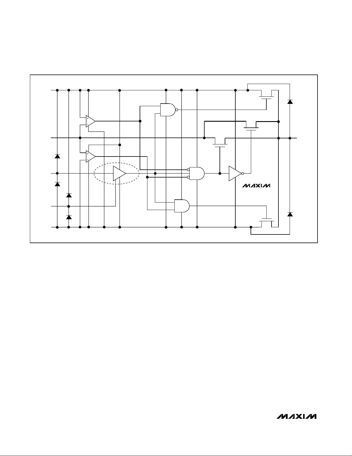
Figure 1 shows the internal construction, with the analog signal paths shown in bold. A single, normally open
(NO) switch is shown. The analog switch is formed by
the parallel combination of N-channel FET N1 and Pchannel FET P1, which are driven on and off simultaneously, according to the input fault condition and the
logic level state.
.
Pin Descriptions
Truth Tables
NAME FUNCTION
1 A0 Address Bit 0
2 EN Enable Input
PIN
3 V- Negative Supply Voltage
4 NO1 Channel Input 1 (fault protected)
10 NO4 Channel Input 4 (fault protected)
7 COM Analog Output
6, 8, 9 N.C. No connection
5 NO2 Channel Input 2 (fault protected)
14 A1 Address Bit 1
13 GND Ground
12 V+ Positive Supply Voltage
11 NO3 Channel Input 3 (fault protected)
MAX4534 (Single 4-to-1 Mux)
MAX4535 (Dual 2-to-1 Mux)
NAME FUNCTION
1 A0 Address Bit 0
2 EN Enable Input
PIN
3 V- Negative Supply Voltage
4 NO1A Channel Input 1A (fault protected)
8 COMB Mux Output B
7 COMA Mux Output A
6, 9, 14 N.C. No connection
5 NO2A Channel Input 2A (fault protected)
13 GND Ground
12 V+ Positive Supply Voltage
11 NO1B Channel Input 1B (fault protected)
10 NO2B Channel Input 2B (fault protected)
X X
0 0
0 1
1 0
1 1
0
1
1
1
1
None
NO1
NO2
NO3
NO4
A0A1 EN ON SWITCH
MAX4534 (Single 4-to-1 Mux)
MAX4535 (Dual 2-to-1 Mux)
_______________________________________________________________________________________ 9
X = Don’t care; logic 0: VAL≤ +0.8; logic 1: VAH≥ +2.4V
X = Don’t care; logic 0: VAL≤ +0.8; logic 1: VAH≥ +2.4V
COMAEN COMBA0
NO2A
NO1A
None
1
1
0
NO2B1
NO1B0
NoneX
Page 10
MAX4534/MAX4535
NO_ Input Voltage
The maximum allowable input voltage for safe operation depends on whether supplies are on or off and on
the load configuration at the COM output. If COM is
referred to a voltage other than ground, but within the
supplies, VNO_ may range higher or lower than the
supplies, provided the absolute value of VNO_ VCOM_ is less than 40V. For example, if the load is
referred to +10V at COM_, then the NO_ voltage range
can be from +50V to -30V. As another example, if the
load is connected to -10V at COM_, the NO_ voltage
range is limited to -50V to +30V.
If the supplies are ±15V and COM is referenced to
ground through a load, the maximum NO_ voltage is
±36V. If the supplies are off and the COM output is referenced to ground, the maximum NO_ voltage is ±40V.
Normal Operation
Two comparators continuously compare the voltage on
the NO_ pin with V+ and V- supply voltages. When the
signal on NO_ is between V+ and V-, the multiplexer
behaves normally, with FETs N1 and P1 turning on and
off in response to A_ signals (Figure 1). The parallel
combination of N1 and P1 forms a low-value resistor
between NO_ and COM_ so that signals pass equally
well in either direction.
Positive Fault Condition
When the signal on NO_ exceeds V+ by about 150mV,
the positive fault comparator output goes high, turning
off FETs N1 and P1 (Figure 1). This makes the NO_ pin
high impedance regardless of the switch state. If the
switch state is “off,” all FETs turn off, and both NO_ and
COM_ are high impedance. If the switch state is “on,”
FET P2 turns on, clamping COM_ to V+.
Negative Fault Condition
When the signal on NO_ goes about 150mV below V-,
the negative fault comparator output goes high, turning
off FETs N1 and P1 (Figure 1). This makes the NO pin
high impedance regardless of the switch state. If the
switch state is “off,” all FETs turn off, and both NO_ and
COM_ are high impedance. If the switch state is “on,”
FET N2 turns on, clamping COM_ to V-.
Fault-Protected, High-Voltage,
Single 4-to-1/Dual 2-to-1 Multiplexers
10 ______________________________________________________________________________________
NORMALLY OPEN SWITCH CONSTRUCTION
COM_
P2
MAX4534
MAX4535
P1
N1
ON
LOW
FAULT
HIGH
FAULT
V+
NO_
A_
GND
ESD DIODE
V-
N2
Figure 1. Functional Diagram
Page 11

MAX4534/MAX4535
Fault-Protected, High-Voltage,
Single 4-to-1/Dual 2-to-1 Multiplexers
______________________________________________________________________________________ 11
Transient Fault Condition
When a fast rising or falling transient on NO_ exceeds
V+ or V-, the output (COM_) follows the input (NO_) to
the supply rail with only a few nanoseconds delay. This
delay is due to the switch on-resistance and circuit
capacitance to ground. When the input transient
returns to within the supply rails, however, there is a
longer output recovery time. For positive faults, the
recovery time is typically 2.5µs. For negative faults, the
recovery time is typically 1.3µs. These values depend
on the COM_ output resistance and capacitance. The
delays do not depend on the fault amplitude. Higher
COM_ output resistance and capacitance increase the
recovery times.
Non-Fault-Protected Pins
FETs N2 and P2 can source about ±10mA from V+ or
V- to the COM_ pin in the fault condition (Figure 1).
Ensure that if the COM_ pin is connected to a low impedance load, the 30mA absolute maximum current
rating is never exceeded, both in normal and fault conditions.
The GND, COM_, EN, and A_ pins do not have fault
protection. Reverse ESD protection diodes are internally connected between GND, COM_, A_, EN, and both
V+ and V-. If a signal on GND, COM_, EN, or A_
exceeds V+ or V- by more than 300mV, one of these
diodes will conduct. During normal operation, these
reverse-biased ESD diodes leak a few nanoamps of
current to V+ and V-.
Fault Protection Voltage and Power-Off
The maximum fault voltage on the NO_ pins is ±40V
from ground when the power is off. With ±15V supply
voltages, the highest voltage on NO_ can be V- + 40V,
and the lowest voltage on NO_ can be V+ - 40V.
Caution: Exceeding these limits can damage the IC.
Logic-Level Thresholds
The logic-level thresholds are CMOS and TTL compatible with V+ = 4.5V to 16.5V.
Applications Information
Ground
There is no connection between the analog signal
paths and GND. The analog signal paths consist of an
N-channel and a P-channel MOSFET with their sources
and drains paralleled, and their gates driven out of
phase to V+ and V- by the logic-level translators.
V+ and GND power the internal logic and logic-level
translators and set the input logic thresholds. The logiclevel translators convert the logic levels to switched V+
and V- signals to drive the gates of the channel
MOSFETs. This drive signal is the only connection
between the power supplies and the analog signals.
GND, A_, EN, and COM_ have ESD protection diodes
to V+ and V-.
Supply Current Reduction
When the logic signals are driven rail-to-rail from 0 to
+15V or -15V to +15V, the current consumption will be
reduced from 300µA (typ) to 180µA.
Power Supplies
The MAX4534/MAX4535 operate with bipolar supplies
between ±4.5V and ±20V. The V+ and V- supplies
need not be symmetrical, but their sum cannot exceed
the 44V absolute maximum rating.
The MAX4534/MAX4535 operate from single supplies
between +9V and +36V when V- is connected to GND.
Page 12

MAX4534/MAX4535
Fault-Protected, High-Voltage,
Single 4-to-1/Dual 2-to-1 Multiplexers
12 ______________________________________________________________________________________
50%
t
OFF(EN)
tR < 20ns
t
F
< 20ns
+3V
0
0
10V
LOGIC
INPUT
V
EN
SWITCH
OUTPUT
V
OUT
V+
V
OUT
V-
GND
V+
A1
V-
A0
EN
NO1
NO2–NO4
COM
+10V
50Ω
MAX4534
R
L
35pF
t
ON(EN)
V+
V
OUT
V-
GND
V+
V-
A0
EN
NO1B
NO1A, NO2A
NO2B, COMA
COMB
+10V
50Ω
MAX4535
R
L
35pF
V
EN
V
EN
90%90%
Figure 2. Address Transition Time
Figure 3. Enable Switching Time
Test Circuits/Timing Diagrams
50%
t
TRANS
tR < 20ns
t
F
< 20ns
V
OUT
+3V
0
V
NO__
V
NO__
LOGIC
INPUT
V
A_
SWITCH
OUTPUT
V+
V
OUT
V-
GND
V+
A1
V-
A0
EN
NO1
NO2, NO3
NO4
COM
+10V
-10V
MAX4534
R
L
35pF
V+
V
OUT
V-
GND
V+
A0
V-
EN
NO1B
NO1A, NO2A
NO2B
COMB
+10V
-10V
MAX4535
R
L
35pF
90%
90%
t
TRANS
ON
+5V
+5V
Page 13

MAX4534/MAX4535
Fault-Protected, High-Voltage,
Single 4-to-1/Dual 2-to-1 Multiplexers
______________________________________________________________________________________ 13
50%
t
OPEN
tR < 20ns
t
F
< 20ns
+3V
0
LOGIC
INPUT
V
A
SWITCH
OUTPUT
V
OUT
V+
V
OUT
V-
GND
V+
A0
V-
A1
EN
NO1–NO4
COM
+10V
50Ω
MAX4534
R
L
35pF
80%
+3V
V
EN
Figure 4. MAX4534 Break-Before-Make Interval
Figure 5. Charge Injection
Figure 6. Off-Isolation
Figure 7. Crosstalk
Test Circuits/Timing Diagrams (continued)
V+
R
S
V
S
CHANNEL
SELECT
NO_
V
EN
EN
A0
A1
V+
MAX4534
GND
+3V
LOGIC
INPUT
0
V
COM
V-
V-
C
1nF
V
OUT
L
EN
V
OUT
IS THE MEASURED VOLTAGE DUE TO CHARGE TRANSFER
∆V
OUT
ERROR V
Q = ∆V
WHEN THE CHANNEL TURNS OFF.
CTE
OUT CL
OFFON ON
∆V
OUT
V
IN
= 50Ω
R
S
NO1
NO4
A0
A1
GND
MAX4534
EN
10nF
V+
10nF
V+
COM
V-
V-
OFF-ISOLATION = 20log
10nF
V+
MAX4534
GND
EN
10nF
V+
COM
R
L
V-
50Ω
V-
CROSSTALK = 20log
V
OUT
V
OUT
V
IN
NO1
NO2
NO4
A0
A1
V
R
IN
1k
V
OUT
R
L
50Ω
V
OUT
IN
V
= 50Ω
R
S
Page 14

MAX4534/MAX4535
Fault-Protected, High-Voltage,
Single 4-to-1/Dual 2-to-1 Multiplexers
Maxim cannot assume responsibility for use of any circuitry other than circuitry entirely embodied in a Maxim product. No circuit patent licenses are
implied. Maxim reserves the right to change the circuitry and specifications without notice at any time.
14 ____________________Maxim Integrated Products, 120 San Gabriel Drive, Sunnyvale, CA 94086 408-737-7600
© 2005 Maxim Integrated Products Printed USA is a registered trademark of Maxim Integrated Products, Inc.
V+
V-
GND
V+
A1
V-
A0
NO4
MAX4534
CHANNEL
SELECT
NO1
COM
EN
1MHz
CAPACITANCE
ANALYZER
Figure 8. NO_, COM_ Capacitance
Figure 9. Transient Behavior of Fault Condition
___________________Chip Information
TRANSISTOR COUNT: 265
Test Circuits/Timing Diagrams (continued)
+25V
VNO_
-15V
-25V
+15V
V
COM_
 Loading...