

Page 1
19-1452; Rev 1; 10/99
For pricing, delivery, and ordering information, please contact Maxim/Dallas Direct! at
1-888-629-4642, or visit Maxim’s website at www.maxim-ic.com.
Quad, Rail-to-Rail, Fault-Protected,
SPDT Analog Switch
General Description
The MAX4533 quad, single-pole/double-throw (SPDT),
fault-protected analog switch is pin-compatible with the
industry-standard MAX333 and MAX333A. The MAX4533
features fault-protected inputs and Rail-to-Rail®signal
handling. The normally open (NO_ ) and normally closed
(NC_ ) terminals are protected from overvoltage faults up
to ±25V with power on and up to ±40V with power off.
During a fault condition, NO_ and NC_ become high
impedance with only nanoamperes of leakage current
flowing to the source. In addition, the output (COM_)
clamps to the appropriate polarity supply rail and provides up to ±10mA of load current. This ensures unambiguous rail-to-rail outputs when a fault occurs.
The MAX4533 operates from dual ±4.5V to ±18V power
supplies or a single +9V to +36V supply. All digital inputs
have +0.8V and +2.4V logic thresholds, ensuring both
TTL and CMOS logic compatibility when using ±15V
supplies or a +12V supply. On-resistance is 175Ω max
and is matched between switches to 10Ω max. The offleakage current is only 0.5nA at T
= +85°C.
T
A
= +25°C and 10nA at
A
Applications
Redundant/Backup Systems Portable Instruments
Test Equipment Data-Acquisition
Communications Systems
Industrial and Process Control Avionics Systems
Systems
Features
♦ Rail-to-Rail Signal Handling
♦ ±40V Fault Protection with Power Off
±25V Fault Protection with ±15V Supplies
♦ All Switches Off with Power Off
♦ No Power-Supply Sequencing Required During
Power-Up or Power-Down
♦ Output Clamped to Appropriate Supply Voltage
During Fault Condition—No Transition Glitch
♦ 1kΩ (typ) Output Clamp Resistance During
Overvoltage
♦ 175Ω (max) Signal Paths with ±15V Supplies
♦ 20ns (typ) Fault Response Time
♦ ±4.5V to ±18V Dual Supplies
+9V to +36V Single Supply
♦ Pin-Compatible with Industry-Standard
MAX333/MAX333A
♦ TTL/CMOS-Compatible Logic Inputs with ±15V or
Single +9V to +15V Supplies
Ordering Information
PART
MAX4533CAP
MAX4533CWP 0°C to +70°C
Ordering Information continued at end of data sheet.
TEMP. RANGE PIN-PACKAGE
0°C to +70°C
20 SSOP
20 Wide SO
MAX4533
†
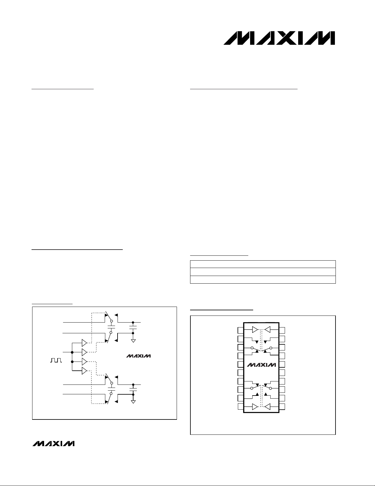
Typical Operating Circuit
Pin Configuration/
Functional Diagram
MAX4533
OUTPUTS
V1 - V2
V3 - V4
TOP VIEW
IN1
1
NO1
2
COM1
3
NC1
4
V-
5
GND
NC2
COM2
NO2
IN2
SWITCHES ARE SHOWN WITH LOGIC "0" INPUT
N.C. = NOT INTERNALLY CONNECTED
MAX4533
6
7
8
9
10
SSOP/SO/DIP/CERDIP
IN4
20
NO4
19
COM4
18
NC4
17
V+
16
N.C.
15
NC3
14
COM3
13
NO3
12
IN3
11
INPUTS
V1
V2
OSC
IN
V3
V4
FLYING CAPACITOR LEVEL TRANSLATOR
Rail-to-Rail is a registered trademark of Nippon Motorola, Ltd.
† Pg
(2-CHANNEL)
________________________________________________________________ Maxim Integrated Products 1
Page 2
MAX4533
Quad, Rail-to-Rail, Fault-Protected,
SPDT Analog Switch
2 _______________________________________________________________________________________
ABSOLUTE MAXIMUM RATINGS
ELECTRICAL CHARACTERISTICS—Dual Supplies
(V+ = +15V, V- = -15V, TA= T
MIN
to T
MAX
, unless otherwise noted. Typical values are at TA= +25°C.) (Note 3)
Stresses beyond those listed under “Absolute Maximum Ratings” may cause permanent damage to the device. These are stress ratings only, and functional
operation of the device at these or any other conditions beyond those indicated in the operational sections of the specifications is not implied. Exposure to
absolute maximum rating conditions for extended periods may affect device reliability.
Voltages Referenced to GND
V+ ........................................................................-0.3V to +44.0V
V- .........................................................................-44.0V to +0.3V
V+ to V-................................................................-0.3V to +44.0V
COM_, IN_ (Note 1) ............................. (V- - 0.3V) to (V+ + 0.3V)
NC_, NO_ (Note 2)..................................(V+ - 40V) to (V- + 40V)
NC_, NO_ to COM_ .................................................-40V to +40V
NC_, NO_ Overvoltage with Switch Power On
(supplies at ±15V) ................................................-30V to +30V
NC_, NO_ Overvoltage with Switch Power Off ........-40V to +40V
Continuous Current into Any Terminal..............................±30mA
Peak Current into Any Terminal
(pulsed at 1ms,10% duty cycle)....................................±50mA
Continuous Power Dissipation (T
A
= +70°C)
20-Pin SSOP (derate 10.53mW/°C above +70°C) ........842mW
20-Pin Wide SO (derate 10.00mW/°C above +70°C) .. 800mW
20-Pin Plastic DIP (derate 11.11mW/°C above +70°C) 889mW
20-Pin CERDIP (derate 11.11mW/°C above +70°C).....889mW
Operating Temperature Ranges
MAX4533C_ _ ......................................................0°C to +70°C
MAX4533E_ _ ...................................................-40°C to +85°C
MAX4533M_ _.................................................-55°C to +125°C
Storage Temperature Range .............................-65°C to +150°C
Lead Temperature (soldering, 10s) .................................+300°C
Note 1: COM_ and IN_ pins are not fault protected. Signals on COM_ or IN_ exceeding V+ or V- are clamped by internal diodes.
Limit forward diode current to maximum current rating.
Note 2: NC_ and NO_ pins are fault protected. Signals on NC_ or NO_ exceeding -25V to +25V may damage the device. These
limits apply with power applied to V+ or V-. The limit is ±40V with V+ = V- = 0.
V
NO
_ or VNC_ = ±10V,
I
COM
_ = 1mA
V+ = +15V, V- = -15V,
VNO_ or VNC_ = ±15V
V
COM_
= +5V, 0, -5V,
I
COM_
= 1mA
CONDITIONS
Ω
125 175
R
ON
COM_ to NO_ or COM_ to NC_
On-Resistance
VV- V+V
NO
_
, V
NC
_
Fault-Free Analog Signal Range
(Note 2)
-200 200
250
Ω4
On-Resistance Flatness
nA
-0.5 0.02 0.5
I
NO_(OFF),
I
NC_(OFF)
NO_ or NC_ Off-Leakage
Current (Note 5)
-10 10
UNITSMIN TYP MAXSYMBOLPARAMETER
+25°C
C, E, M
M
M
+25°C
+25°C
C, E
T
A
C, E 200
+25°C
VNO_ or VNC_ = ±10V,
I
COM
_ = 1mA
M
C, E 10
Ω
16
∆
R
ON
COM_ to NO_ or COM_ to NC_
On-Resistance Match Between
Channels (Note 4)
15
M
VNO_ or VNC_ = ±14V,
V
COM
_ = 14V
V
COM_
= ±14V,
V
NO_
or V
NC_
= ±14V or floating
+25°C
C, E
-400 400
nA
-0.5 0.01 0.5
I
COM_(ON)
COM_ On-Leakage Current
(Note 5)
-20 20
+25°C -25 +25Applies with power on
V
NO_
, V
NC_
V
Fault-Protected Analog Signal
Range (Note 2)
M
VNO_ or VNC_ = ±25V,
V
COM
_ = 10V
V
NO_
or V
NC_
= ±25V,
no connection to “ON” channel
+25°C
C, E
-10 10
-10 10
-200 200
I
COM_
nA
COM_ Output Leakage Current,
Supplies On
M
+25°C
C, E
-10 10
-20 20
I
NO_, INC_
-200 200
µA
nA
NO_ or NC_ Off Input Leakage
Current, Supplies On
Applies with power off +25°C -40 +40
µA
FAULT
ANALOG SWITCH
±
±
Page 3
MAX4533
Quad, Rail-to-Rail, Fault-Protected,
SPDT Analog Switch
_______________________________________________________________________________________ 3
ELECTRICAL CHARACTERISTICS—Dual Supplies (continued)
(V+ = +15V, V- = -15V, TA= T
MIN
to T
MAX
, unless otherwise noted. Typical values are at TA= +25°C.) (Note 3)
CONDITIONS T
A
UNITSMIN TYP MAXSYMBOLPARAMETER
+25°C
+25°C
C, E
1.0 2.5
-20 0.1 20
I
NO_, INC_
-200 200
NO_ or NC_ Input Leakage
Current, Supplies Off
COM_ On-Clamp Output
Resistance, Supplies On
nA
+25°C
V
NO_
or VNC= ±25V
C, E, M
20
3
R
COM_
ns
kΩ
RL= 10kΩ,
V
NO_
or V
NC_
= ±25V
±Fault Output Clamp Turn-On
Delay Time (Note 6)
C, E, M 2.4 VV
IN_H
IN_ Input Logic Threshold High
+25°C 100 250
C, E 400
M
+25°C
600
10 50
V
COM_
= ±10V,
R
L
= 1kΩ; Figure 3
t
BBM
Break-Before-Make Time Delay ns
RL= 10kΩ,
V
NO_
or V
NC_
= ±25V
+25°C 2.5 µs
±Fault Recovery Time
(Note 6)
C, E, M 0.8 VV
IN_L
IN_ Input Logic Threshold Low
V
IN_
= +0.8V or +2.4V
+25°C -1 0.03 1
I
IN_H, IIN_L
µA
IN_ Input Current Logic High or
Low
C, E, M -5 5
V
COM_
= ±10V,
R
L
= 2kΩ; Figure 2
t
ON
Turn-On Time ns
RL= 50Ω, CL= 15pF,
V
N_
= 1V
RMS
, f = 1MHz;
Figure 6
f = 1MHz; Figure 5
V
ISO
C
N_(OFF)
Off-Isolation (Note 7)
NO_ or NC_ Off-Capacitance
dB
pF+25°C 5
+25°C -62
+25°C
60 150
V
NO_
= ±10V,
RL= 2kΩ; Figure 2
t
OFF
Turn-Off Time
ns
C, E 300
M
450
±4.5 ±18 VV+, V-Power-Supply Range
C, E, M
+25°C
600
400
µA
All V
IN_
= 0 or +5V,
V
NO_
= V
NC_
= 0
C, E, M
+25°C
1000
600
µA
All V
IN_
= 0 or +5V,
V
NO_
= V
NC_
= 0
I+V+ Supply Current
I-V- Supply Current
+25°C 1.5
CL= 100pF,
V
COM_
= 0; Figure 4
Q pCCharge Injection (Note 6)
f = 1MHz; Figure 5C
COM_(ON)
COM_ On-Capacitance pF+25°C 12
RL= 50Ω, CL= 15pF,
VN_= 1V
RMS
, f = 1MHz;
Figure 6
V
CT
Channel-to-Channel Crosstalk
(Note 8)
dB+25°C -66
C, E, M
+25°C
450
300
µA
All V
IN_
= 0 or +5V,
V
NO_
= V
NC_
= 0
I
GND
GND Supply Current
V
NO_
or V
NC_
= +25V +25°C
+25°C
81113
I
COM_
-12 -10 -7
COM_ On-Clamp Output
Current, Supplies On
V
NO_
or V
NC_
= -25V
mA
V
NO_
or V
NC_
= ±40V,
V+ = 0, V- = 0
M
-10 10 µA
LOGIC INPUT
SWITCH DYNAMIC CHARACTERISTICS
POWER SUPPLY
Page 4
MAX4533
Quad, Rail-to-Rail, Fault-Protected,
SPDT Analog Switch
4 _______________________________________________________________________________________
ELECTRICAL CHARACTERISTICS—Single Supply
(V+ = +12V, V- = 0, TA= T
MIN
to T
MAX
, unless otherwise noted. Typical values are at TA= +25°C.) (Note 3)
+25°C
C, E, M
V+ = +12V,
V
NO
_ or VNC_ = +10V,
I
COM
_ = 1mA
M
V+ = +12V,
V
COM_
= +10V,
V
NO_
or V
NC_
= +10V or floating
V+ = +12V, V- = 0,
VNO_ or VNC_ = +12V or 0
+25°C
C, E
-400 400
M
nA
-0.5 0.01 0.5
I
COM_(ON)
COM_ On-Leakage Current
(Notes 5, 9)
-20 20
Applies with power off
+25°C
V+ = +12V,
V
COM_
= +10V, +1V,
V
NO_
or V
NC_
= +1V, +10V
+25°C
CONDITIONS
M
+25°C
+25°C
C, E
T
A
C, E
V+ = +12V,
V
NO
_ or VNC_ = +10V,
I
COM
_ = 1mA
M
450
C, E 20
Ω
410
∆R
ON
COM_ -NO_ On-Resistance
Match Between Channels
(Note 4)
30
-40 +40
-25 +25
µA
Applies with power on
V
NO_
, V
NC_
M
V
V
NO_
or V
NC_
= ±40V,
V+ = 0, V- = 0
Fault-Protected Analog Signal
Range (Note 2)
M
V
NO_
or V
NC_
= ±25V,
V+ = +12V,
no connection to “ON” channel
+25°C
C, E
-10 10
+25°C
-10 10
C, E
-10 10
-200 200
-20 0.1 20
I
NO_, INC_
-200 200
I
COM_
µA
nA
COM_ Output Leakage Current,
Supply On (Note 9)
nA
M
V
NO_
or V
NC_
= ±25V,
V
COM_
= 0,
V+ = +12V
+25°C
C, E
Ω
260 390
R
ON
COM_ to NO_, COM_ to NC_
On-Resistance
V0V+V
NO
_
, V
NC
_
Fault-Free Analog Signal Range
(Note 2)
-10 10
NO_ or NC_ Input Leakage
Current, Supply Off (Note 9)
-20 20
I
NO_, INC_
-200 200
µA
nA
NO_ or NC_ Off Input Leakage
Current, Supply On (Note 9)
-200 200
525
nA
-0.5 0.01 0.5
I
NO_(OFF),
I
NC_(OFF)
NO_ or NC_ Off-Leakage
Current (Notes 5, 9)
-10 10
UNITSMIN TYP MAXSYMBOLPARAMETER
+25°C 235
V
NO_
or V
NC_
= ±25V,
V+ = +12V
I
COM_
mA
COM_ On-Clamp Output
Current, Supply On
+25°C
C, E, M
C, E, M
-1 0.03 1
2.4V
IN_H
0.8
µA
VIN_ Input Logic Threshold High
V
IN_
= +0.8V or +2.4VI
IN_H, IIN_L
V
IN_L
V
IN_ Input Current Logic High or
Low
IN_ Input Logic Threshold Low
+25°C 2.4 5
V
NO_
or V
NC_
= ±25V,
V+ = +12V
R
COM_
kΩ
COM_ On-Clamp Output
Resistance, Supply On
C, E, M -5 5
ANALOG SWITCH
FAULT
LOGIC INPUT
Page 5

MAX4533
Quad, Rail-to-Rail, Fault-Protected,
SPDT Analog Switch
_______________________________________________________________________________________ 5
Note 3: The algebraic convention is used in this data sheet; the most negative value is shown in the minimum column.
Note 4: ∆R
ON
= R
ON(MAX)
- R
ON(MIN)
.
Note 5: Leakage parameters are 100% tested at maximum-rated hot temperature and guaranteed by correlation at T
A
= +25°C.
Note 6: Guaranteed by design.
Note 7: Off-isolation = 20log10(V
COM_
/ V
NO_
), V
COM_
= output, V
NO_
= input to off switch.
Note 8: Between any two analog inputs.
Note 9: Leakage testing for single-supply operation is guaranteed by testing with dual supplies.
ELECTRICAL CHARACTERISTICS—Single Supply (continued)
(V+ = +12V, V- = 0, TA= T
MIN
to T
MAX
, unless otherwise noted. Typical values are at TA= +25°C.) (Note 3)
CONDITIONS T
A
+25°C 200 500
V
COM_
= +10V,
RL= 2kΩ; Figure 2
t
ON
Turn-On Time ns
C, E, M
+25°C
550
350
f = 1MHz; Figure 5
C, E, M
C
COM_(ON)
1000
RL= 50Ω, CL= 15pF,
V
NO_
= 1V
RMS
, f = 1MHz;
Figure 6
f = 1MHz; Figure 5
V
ISO
C
N_(OFF)
Off-Isolation (Note 7)
NO_ or NC_ Off-Capacitance
dB
µA
pF
All V
IN_
= 0 or +5V,
V
NO_
= V
NC_
= 0
C, E, M
I
GND
+25°C
V- and GND Supply Current
5 100
936
V
COM_
= +10V,
RL= 1kΩ; Figure 3
V
t
BBM
Break-Before-Make Time Delay ns
+25°C 5
RL= 50Ω, CL= 15pF,
V
NO_
= 1V
RMS
, f = 1MHz;
Figure 6
COM_ On-Capacitance
+25°C
V
CT
UNITSMIN TYP MAXSYMBOLPARAMETER
Channel-to-Channel Crosstalk
(Note 8)
-62
pF
dB+25°C
+25°C 15
-65
V+Power-Supply Range
C, E, M
+25°C
350
200
µA
All V
IN_
= 0 or +12V,
V
NO_
= V
NC_
= 0
C, E, M
+25°C
550
350
µA
All V
IN_
= 0 or +5V,
V
NO_
= V
NC_
= 0
I+V+ Supply Current
+25°C 2
CL= 100pF,
V
COM_
= 0; Figure 4
Q pCCharge Injection
+25°C 100 300
V
COM_
= +10V,
R
L
= 2kΩ; Figure 2
t
OFF
Turn-Off Time ns
C, E, M 900
SWITCH DYNAMIC CHARACTERISTICS
POWER SUPPLY
Page 6

MAX4533
Quad, Rail-to-Rail, Fault-Protected,
SPDT Analog Switch
6 _______________________________________________________________________________________
Typical Operating Characteristics
(V+ = +15V, V- = -15V, TA = +25°C, unless otherwise noted.)
0
90
60
30
120
150
210
180
240
270
300
330
360
390
-18 -12 -9-15 -6-30369121518
ON-RESISTANCE vs. V
COM
(DUAL SUPPLIES)
MAX4533 toc01
V
COM
(V)
R
ON
(Ω)
V± = ±4.5V
V± = ±10V
V± = ±12V
V± = ±15V
V± = ±18V
0
100
50
200
150
250
300
350
400
010155 2025303540
ON-RESISTANCE vs. V
COM
(SINGLE SUPPLY)
MAX4533toc02
V
COM
(V)
R
ON
(Ω)
V- = 0
V+ = +12V
V+ = +15V
V+ = +20V
V+ = +25V
V+ = +30V
V+ = +36V
V+ = +9V
0
75
50
25
100
125
150
175
200
225
250
-15 -5-10 0 5 10 15
ON-RESISTANCE vs. V
COM
AND
TEMPERATURE (DUAL SUPPLIES)
MAX4533 toc03
V
COM
(V)
R
ON
(Ω)
V+ = +15V
V- = -15V
TA = +85°C
TA = +125°C
TA = +70°C
TA = +25°C
TA = 0°C
TA = -40°C
TA = -55°C
0
100
50
250
200
150
400
350
300
450
042681012
ON-RESISTANCE vs. V
COM
AND
TEMPERATURE (SINGLE SUPPLY)
MAX4533 toc04
V
COM
(V)
R
ON
(Ω)
TA = +125°C
TA = +70°C
TA = +85°C
TA = -40°C
TA = 0°C
TA = -55°C
TA = +25°C
V+ = +12V
V- = 0
0
200
100
400
300
500
600
±4 ±10 ±12±6 ±8 ±14 ±16 ±18
TURN-ON/TURN-OFF TIME vs.
SUPPLY VOLTAGE (DUAL SUPPLIES)
MAX4533 toc07a
SUPPLY VOLTAGE (V)
t
ON
, t
OFF
(ns)
t
ON
t
OFF
0.0001
0.01
0.001
1
0.1
100
10
1000
-55 -15 5-35 25 45 65 85 105 125
ON/OFF-LEAKAGE CURRENT
vs. TEMPERATURE
MAX4533 toc05
TEMPERATURE (°C)
LEAKAGE CURRENT (A)
I
COM_ON
(V+ = +15V, V- = -15V)
I
COM_ON
(V+ = +12V, V- = 0)
I
NC_OFF
(V+ = +12V, V- = 0)
I
NC_OFF
(V+ = +15V, V- = -15V)
0
1.0
0.5
2.0
1.5
3.0
2.5
3.5
4.5
4.0
5.0
-15 -10 -5 0 15510
CHARGE INJECTION vs. V
COM
MAX4533 toco6
V
COM
(V)
Q (pC)
SINGLE SUPPLY
DUAL SUPPLIES
0
50
150
100
200
250
81612 20 24 28 32 36
TURN-ON/TURN-OFF TIME vs.
SUPPLY VOLTAGE (SINGLE SUPPLY)
MAX4533 toc07b
SUPPLY VOLTAGE (V)
t
ON
, t
OFF
(ns)
t
ON
t
OFF
0
40
20
80
60
120
100
140
180
160
200
-55 -15 5 25-35 45 65 85 105 125
TURN-ON/TURN-OFF TIME vs.
TEMPERATURE (DUAL SUPPLIES)
MAX4533 toc08a
TEMPERATURE (°C)
t
ON
, t
OFF
(ns)
t
ON
t
OFF
V+ = +15V
V- = -15V
Page 7

MAX4533
Quad, Rail-to-Rail, Fault-Protected,
SPDT Analog Switch
_______________________________________________________________________________________ 7
)
Typical Operating Characteristics (continued)
(V+ = +15V, V- = -15V, TA = +25°C, unless otherwise noted.)
COM_
(10V/div)
NO_ or
NC_
(10V/div)
OV
OV
FAULT-FREE SIGNAL WITH ±15V INPUT
MAX4533 toc12
5µs/div
COM_
(10V/div)
NO_ or
NC_
(10V/div)
OV
OV
FAULT RECOVERY TIME
MAX4533 toc13
2µs/div
TURN-ON/TURN-OFF TIME vs.
TEMPERATURE (SINGLE SUPPLY)
250
200
150
(ns)
OFF
, t
ON
t
100
50
0
-55 25 45-15 5-35 65 85 105 125
t
ON
t
OFF
TEMPERATURE (°C)
V+ = +12V
POWER-SUPPLY CURRENT vs.
TEMPERATURE (SINGLE SUPPLY)
400
350
300
250
200
150
SUPPLY CURRENT (µA)
100
50
0
-55 5 25-35 -15 45 65 85 105 125
I+
I
GND
TEMPERATURE (°C
V- = 0
V+ = +12V
V- = 0
= +5V
V
IN
MAX4533 toc08b
-100
-200
SUPPLY CURRENT (µA)
-300
-400
-500
MAX4533 toc09c
LOGIC-LEVEL THRESHOLD (V)
POWER-SUPPLY CURRENT vs.
TEMPERATURE (DUAL SUPPLIES, V
500
400
300
200
100
0
-55 -15 5 25-35 45 65 85 105 125
LOGIC-LEVEL THRESHOLD
3.0
2.5
DUAL-SUPPLY
RANGE
2.0
1.5
1.0
0.5
0
4 8 12 16 20 24 28 32 36
I+
I
GND
I-
TEMPERATURE (°C)
vs. SUPPLY VOLTAGE
SINGLE-SUPPLY
RANGE
SUPPLY VOLTAGE (V)
V+ = +15V
V- = -15V
IN
= 0)
MAX4533 toc09a
MAX4533 toc10
(10V/div)
(10V/div)
POWER-SUPPLY CURRENT vs.
TEMPERATURE (DUAL SUPPLIES, V
800
600
400
200
0
SUPPLY CURRENT (µA)
-200
-400
-600
-55 -15 5-35 25 45 65 85 105 125
I+
I
GND
I-
TEMPERATURE (°C)
OVERVOLTAGE WITH ±25V INPUT
NO_ or
NC_
OV
COM_
OV
5µs/div
IN
V+ = +15V
V- = -15V
= +5V)
MAX4533 toc09b
MAX4533 toc11
Page 8

MAX4533
Quad, Rail-to-Rail, Fault-Protected,
SPDT Analog Switch
8 _______________________________________________________________________________________
Typical Operating Characteristics (continued)
(V+ = +15V, V- = -15V, TA = +25°C, unless otherwise noted.)
0
-100
0.01 0.1 1 10 100 1000
FREQUENCY RESPONSE
(SINGLE SUPPLY)
-80
-90
-70
MAX4533 toc14b
FREQUENCY (MHz)
RESPONSE (dB)
-60
-50
-40
-30
-10
-20
BANDWIDTH
V+ = +12V
V- = 0
CROSSTALK
OFF ISOLATION
Pin Description
Detailed Description
The MAX4533 is a fault-protected analog switch with
special operation and construction. Traditional fault-protected switches are constructed using three-series
CMOS devices. This combination produces good fault
protection but fairly high on-resistance when the signals
are within about 3V of each supply rail. These series
devices are not capable of handling signals up to the
power-supply rails.
The MAX4533 differs considerably from traditional faultprotected switches, with three advantages. First, it is
constructed with two parallel FETs, allowing very low
on-resistance when the switch is on. Second, they allow
signals on the NC_ or NO_ pins that are within or slightly
beyond the supply rails to be passed through the switch
to the COM_ terminal, allowing rail-to-rail signal operation. Third, when a signal on NC_ or NO_ exceeds the
supply rails by about 150mV (a fault condition), the voltage on COM_ is limited to the appropriate polarity supply voltage. Operation is identical for both fault
polarities. The fault-protection extends to ±25V with
power on and ±40V with power off.
The MAX4533 has a parallel N-channel and P-channel
MOSFET switch configuration with input voltage sensors.
The simplified internal structure is shown in Figure 1. The
parallel N1 and P1 MOSFETs form the switch element.
N3 and P3 are sensor elements to sample the input voltage and compare it against the power-supply rails.
NAME FUNCTION
1, 10, 11, 20 IN1, IN2, IN3, IN4 Logic Control Digital Inputs
PIN
2, 9, 12, 19 NO1, NO2, NO3, NO4 Normally Open Inputs*
3, 8, 13, 18 COM1, COM2, COM3, COM4 Analog Switch Common Outputs*
4, 7, 14, 17 NC1, NC2, NC3, NC4 Normally Closed Inputs*
5 V- Negative Analog Supply Voltage Input
6 GND Digital Ground
15 N.C. No Connection. Not internally connected.
16 V+ Positive Analog and Digital Supply-Voltage Input
*When the voltage on NO_ or NC_ does not exceed V+ or V-, NO_ (or NC_) and COM_ pins are bidirectional.
0
-10
-20
-30
-40
-50
-60
RESPONSE (dB)
-70
-80
-90
-100
0.01 0.1 1 10 100 1000
FREQUENCY RESPONSE
(DUAL SUPPLIES)
BANDWIDTH
MAX4533 toc14a
OFF ISOLATION
CROSSTALK
V+ = +15V
V- = -15V
FREQUENCY (MHz)
Page 9

During normal operation of a conducting channel, N1
and P1 remain on with a typical 125Ω on-resistance
between NO_ (or NC_) and COM_. If the input voltage
exceeds either supply rail by about 150mV, the parallel
combination switches (N1, P1) are forced off through
the driver and sensing circuitries. At the same time, the
output (COM_ ) is clamped to the appropriate supply
rail by the clamp circuitries (N2, P2). Two clamp circuits
limit the output voltage to the supply voltages.
For simplicity, Figure 1 shows only one side of the SPDT
switch configuration. The complete circuit is composed
of two channels with their outputs connected.
Normal Operation
Two comparators continuously compare the voltage on
the NO_ (or NC_ ) pin with V+ and V- supply voltages.
When the signal on NO_ (or NC_ ) is between V+ and
V-, the switch behaves normally, with FETs N1 and P1
turning on and off in response to NO_ (or NC_) signals
(Figure 1). For any voltage between the supply rails,
the switch is bidirectional; therefore, COM_ and NC_
(or NO_ ) are interchangeable. Only NO_ and NC_ can
be exposed to overvoltages beyond the supply range
and within the specified breakdown limits of the device.
Fault Condition
The MAX4533 protects devices connected to its output
(COM_) through its unique fault-protection circuitry.
When the input voltage is raised above either supply
rail, the internal sense and comparator circuitries (N3
and N-channel driver or P3 and P-channel driver) disconnect the output (COM_) from the input (Figure 1).
If the switch driven above the supply rail has an on
state, the clamp circuitries (N2 or P2) connect the output to the appropriate supply rail. Table 1 summarizes
the MAX4533’s operation under normal and fault conditions. Row 5 shows a negative fault condition when the
supplies are on. It shows that with supplies of ±15V, if
the input voltage is between -15V and -25V, the output
(COM_) clamps to the negative supply rail of -15V.
With this technique, the SPDT switch is capable of withstanding a worse-case condition of opposite fault polarities at its inputs.
Transient Fault Condition
When a fast rising or falling transient on NO_ (or NC_)
exceeds V+ or V-, the output (COM_) follows the input
(IN_) to the supply rail by only a few nanoseconds. This
delay is due to the switch on-resistance and circuit
capacitance to ground. However, when the input transient returns to within the supply rails there is a longer
recovery time. For positive faults, the recovery time is
typically 2.5µs. For negative faults, the recovery time is
typically 1.3µs. These values depend on the COM_ output resistance and capacitance. The delays are not
dependent on the fault amplitude. Higher COM_ output
resistance and capacitance increase the recovery
times.
Fault Protection, Voltage, and Power Off
The maximum fault voltage on the NO_ or NC_ pins is
±40V from ground when the power is off. With ±15V supply voltages, the highest voltage on NO_ (or NC_) can
be +25V, and the lowest voltage on NO_ (or NC_) can
be -25V. Exceeding these limits can damage the chip.
IN_ Logic-Level Thresholds
The logic-level thresholds are TTL/CMOS-compatible
when V+ is +15V. Raising V+ increases the threshold
slightly; when V+ reaches +25V, the level threshold is
2.8V—higher than the TTL output high-level minimum of
2.4V, but still compatible with CMOS outputs (see the
Typical Operating Characteristics).
Increasing V- has no effect on the logic-level thresholds, but it does increase the gate-drive voltage to the
signal FETs, reducing their on-resistance.
MAX4533
Quad, Rail-to-Rail, Fault-Protected,
SPDT Analog Switch
_______________________________________________________________________________________ 9
Figure 1. Simplified Internal Structure
-15V
-15V
NC_
or
INPUT
NO_
+15V
+15V
N3
SENSE
SWITCH
SENSE
SWITCH
COMPARATOR
N-CHANNEL
DRIVER
P3
P-CHANNEL
DRIVER
COMPARATOR
-V(-15V)
N2
CLAMP
N1
P1
CLAMP
+V(+15V)
OUTPUT COM_
P2
Page 10

Failure Modes
The MAX4533 is not a lightning arrester or surge protector. Exceeding the fault-protection voltage limits on
NO_ or NC_, even for very short periods, can cause the
device to fail.
Applications Information
Ground
There is no connection between the analog signal
paths and GND. The analog signal paths consist of an
N-channel and P-channel MOSFET with their sources
and drains paralleled and their gates driven out of
phase to V+ and V- by the logic-level translators.
V+ and GND power the internal logic and logic-level
translators and set the input logic thresholds. The logiclevel translators convert the logic levels to switched V+
and V- signals to drive the gates of the switches. This
drive signal is the only connection between the power
supplies and the analog signals. GND, IN_, and COM_
have ESD protection diodes to V+ and V-.
Supply Current Reduction
When the logic signals are driven rail-to-rail from 0 to
+12V or -15V to +15V, the supply current reduces to
approximately half of the supply current when the logic
input levels are at 0 to 5V.
Power Supplies
The MAX4533 operates with bipolar supplies between
±4.5V and ±18V. The V+ and V- supplies need not be
symmetrical, but their difference can not exceed the
absolute maximum rating of +44V. The MAX4533 operates from a single supply between +9V and +36V when
V- is connected to GND.
MAX4533
Quad, Rail-to-Rail, Fault-Protected,
SPDT Analog Switch
10 ______________________________________________________________________________________
Table 1. Switch States in Normal and Fault Conditions
INPUT
RANGE
On Between Rails
POWER
SUPPLIES
(V+, V-)
NC_
On
NO_
Off
OUTPUT
NC_
On Between Rails Off On NO_
On Between V+ and (+40V - V+) On Off V+
On Between V+ and (+40V - V+) Off On V+
On Between V- and (-40V - V-) On Off V-
On Between V- and (-40V - V-) Off On V-
Off Between Rails Off Off
Follows the load
terminal voltage.
Test Circuits/Timing Diagrams
Figure 2. Switching-Time Test Circuit
tR < 20ns
t
< 20ns
3V
V
IN
0V
+10V
V
COM
0V
-10V
t
OFF
F
50%
t
OFF
t
OPEN
50% 50%
50% 50%
t
ON
50%
t
ON
t
OPEN
MAX4533
+10V
-10V
IN_
LOGIC
INPUT
(REPEAT TEST FOR IN2, IN3, AND IN4.)
V+
+15V
NC_
NO_
GND
COM_
V-
-15V
SWITCH OUTPUT
2kΩ
Page 11

MAX4533
Quad, Rail-to-Rail, Fault-Protected,
SPDT Analog Switch
______________________________________________________________________________________ 11
Test Circuits/Timing Diagrams (continued)
Figure 3. Break-Before-Make
Figure 4. Charge Injection
Figure 5. COM_, NO_, NC_ Capacitance
V
V
+3V
COM
COM
0V
V
0V
V
O2
0V
LOGIC
INPUT
SWITCH
OUTPUT
SWITCH
OUTPUT
V
IN_
IN_
50Ω
O1
50%
t
D
0.9V
V+
V+
MAX4533
NC_ OR NO_
GND
+15V
GND
IN_
V+
V+
0V
V
OUT
V-
-15V
NO
R
L2
V
O2
RL = 1000Ω
CL = 35pF
C
NC
V
O1
∆ V
OUT
C
L1
R
L1
L2
MAX4533
V
COM_
COM
O
LOGIC
INPUT
V
OUT
V
V-
COM_
0.9V
O
t
D
C
L
100pF
IN_
CL INCLUDES FIXTURE AND STRAY CAPACITANCE.
LOGIC 0 INPUT.
V
V-
V- IS CONNECTED TO GND (0V) FOR SINGLE-SUPPLY OPERATION. Q = ∆ V
V+
V+
V+
MAX4533
ADDRESS SELECT
V- IS CONNECTED TO GND (0V) FOR SINGLE-SUPPLY OPERATION.
IN_
GND
NO_
NC_
COM_
V-
V-
∆ V
IS THE MEASURED VOLTAGE DUE TO CHARGE-
OUT
TRANSFER ERROR Q WHEN THE CHANNEL TURNS OFF.
x C
OUT
L
1MHz
CAPACITANCE
ANALYZER
Page 12

MAX4533
Quad, Rail-to-Rail, Fault-Protected,
SPDT Analog Switch
Maxim cannot assume responsibility for use of any circuitry other than circuitry entirely embodied in a Maxim product. No circuit patent licenses are
implied. Maxim reserves the right to change the circuitry and specifications without notice at any time.
12 ____________________Maxim Integrated Products, 120 San Gabriel Drive, Sunnyvale, CA 94086 408-737-7600
© 1999 Maxim Integrated Products Printed USA is a registered trademark of Maxim Integrated Products.
Test Circuits/Timing Diagrams (continued)
Figure 6. Frequency Response, Off-Isolation, and Crosstalk
PART
MAX4533CPP 0°C to +70°C
TEMP. RANGE PIN-PACKAGE
20 Plastic DIP
MAX4533EAP
MAX4533EWP
MAX4533EPP -40°C to +85°C
-40°C to +85°C
-40°C to +85°C 20 SSOP
20 Wide SO
20 Plastic DIP
MAX4533MJP -55°C to +125°C 20 CERDIP
Ordering Information (continued)
Chip Information
TRANSISTOR COUNT: 448
V+
10nF
NETWORK
ANALYZER
50Ω
MEAS. REF.
50Ω 50Ω
50Ω
ADDRESS SELECT
MEASUREMENTS ARE STANDARDIZED AGAINST SHORTS AT SOCKET TERMINALS.
OFF ISOLATION IS MEASURED BETWEEN COM_ AND “OFF” NO_ OR NC_ TERMINALS.
ON LOSS IS MEASURED BETWEEN COM_ AND “ON” NO_ OR NC_ TERMINALS.
CROSSTALK IS MEASURED BETWEEN COM_ TERMINALS WITH ALL SWITCHES ON.
SIGNAL DIRECTION THROUGH SWITCH IS REVERSED; WORST VALUES ARE RECORDED.
V- IS CONNECTED TO GND (0V) FOR SINGLE-SUPPLY OPERATION.
IN_
V+
MAX4533
GND
COM_
NO_, NC_
10nF
V
IN
V
OUT
V-
V-
OFF ISOLATION = 20 log
ON LOSS = 20 log
CROSSTALK = 20 log
V
OUT
V
IN
V
OUT
V
IN
V
OUT
V
IN
 Loading...