For free samples & the latest literature: http://www.maxim-ic.com, or phone 1-800-998-8800.
For small orders, phone 408-737-7600 ext. 3468.
General Description
The MAX4529 is a low-voltage T-switch designed for
switching RF and video signals from DC to 300MHz in
50Ω and 75Ω systems. This switch is constructed in a
“T” configuration, ensuring excellent high-frequency off
isolation of -80dB at 10MHz.
The MAX4529 can handle Rail-to-Rail®analog signals
in either direction. On-resistance (70Ω max) is flat (0.5Ω
max) over the specified signal range, using ±5V supplies. The off leakage current is less than 1nA at +25°C
and 20nA at +85°C.
This CMOS switch can operate with dual power supplies ranging from ±2.7V to ±6V or a single supply
between +2.7V and +12V. All digital inputs have
0.8V/2.4V logic thresholds, ensuring both TTL- and
CMOS-logic compatibility when using ±5V or a single
+5V supply.
________________________Applications
RF Switching
Video Signal Routing
High-Speed Data Acquisition
Test Equipment
ATE Equipment
Networking
____________________________Features
♦ High 50Ω Off Isolation: -80dB at 10MHz
♦ DC to 300MHz -3dB Signal Bandwidth
♦ 70Ω Signal Paths with ±5V Supplies
♦ 10Ω Signal-Path Flatness with ±5V Supplies
♦ ±2.7V to ±6V Dual Supplies
+2.7V to +12V Single Supply
♦ Low Power Consumption: <1µW
♦ Rail-to-Rail Bidirectional Signal Handling
♦ >2kV ESD Protection per Method 3015.7
♦ TTL/CMOS-Compatible Inputs with
Single +5V or ±5V
MAX4529
Low-Voltage, Bidirectional
RF/Video Switch
________________________________________________________________
Maxim Integrated Products
1
8
7
6
5
1
2
3
4
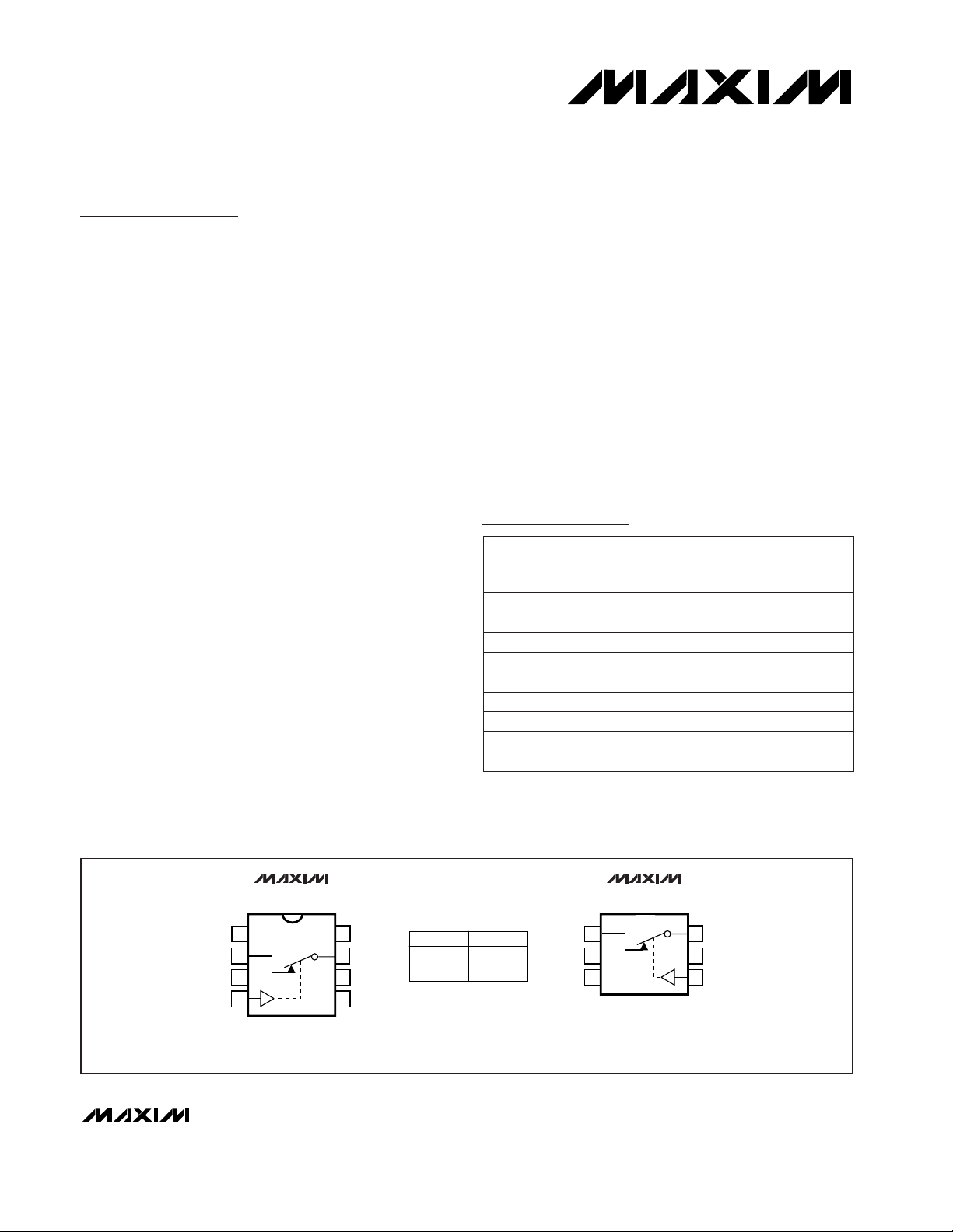
MAX4529
DIP/SO/µMAX
V+
COM
N.C.
V-IN
GND
NC
N.C.
N.C. = NOT INTERNALLY CONNECTED
LOGIC SWITCH
0
1
ON
OFF
6
5
4
1
2
3
MAX4529
SOT23-6
COM
GND
INV-
V+
NC
_______________________Pin Configurations/Functional Diagrams/Truth Table
19-1262; Rev 0; 3/98
Ordering Information
*
Contact factory for dice specifications.
Rail-to-Rail is a registered trademark of Nippon Motorola Ltd.
PART
MAX4529CPA
MAX4529CSA 0°C to +70°C
0°C to +70°C
TEMP. RANGE
PINPACKAGE
8 Plastic DIP
8 Narrow SO
SOT
TOP MARK
—
—
MAX4529CUA
MAX4529
CUT-T—0°C to +70°C
0°C to +70°C 8 µMAX
6 SOT23-6 AAAQ
MAX4529C/D
MAX4529EPA—-40°C to +85°C
0°C to +70°C Dice*
8 Plastic DIP —
MAX4529ESA
MAX4529EUA—-40°C to +85°C
-40°C to +85°C 8 Narrow SO
8 µMAX —
MAX4529
EUT-T
-40°C to +85°C 6 SOT23-6 AAAQ

MAX4529
Low-Voltage, Bidirectional
RF/Video Switch
2 _______________________________________________________________________________________
ABSOLUTE MAXIMUM RATINGS
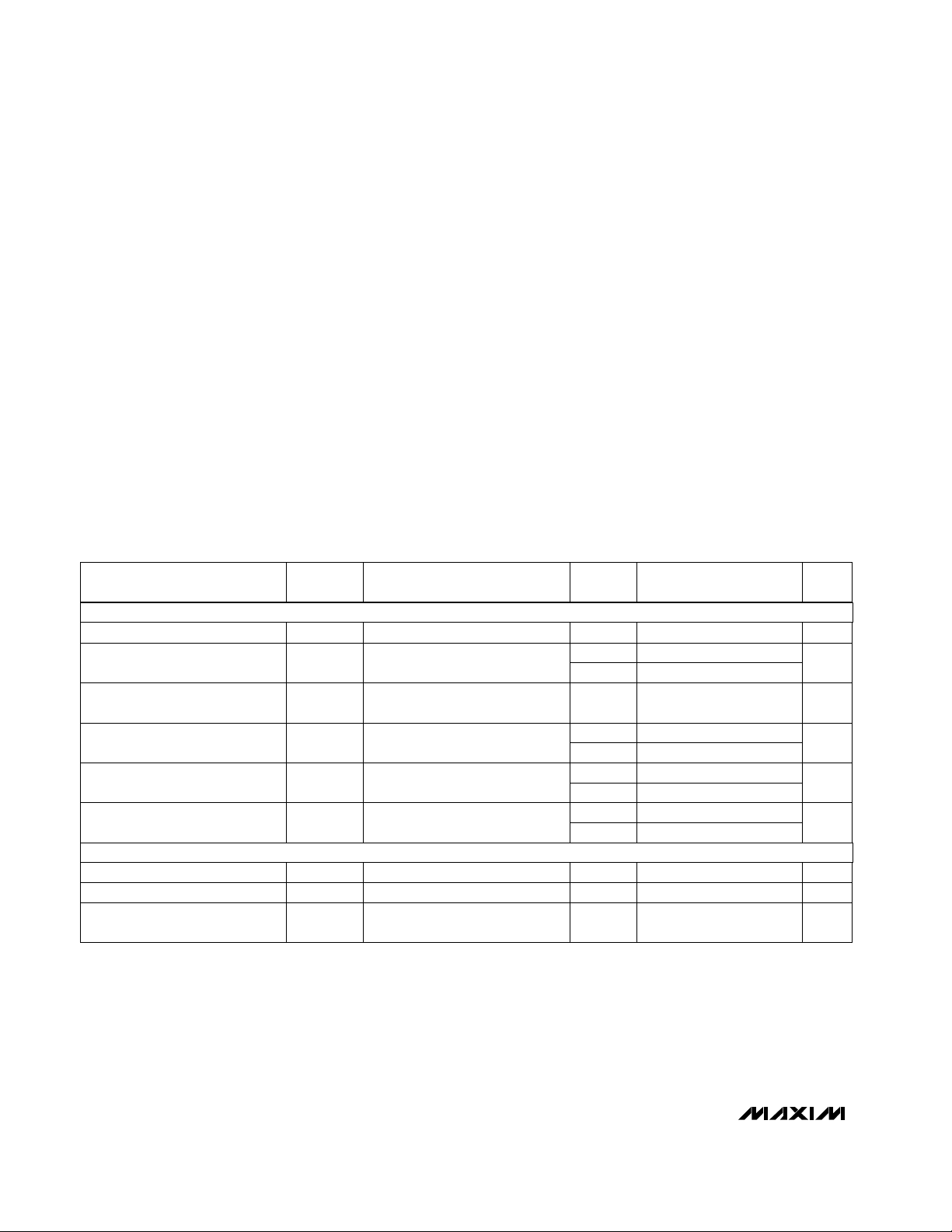
ELECTRICAL CHARACTERISTICS—Dual Supplies
(V+ = +4.5V to +5.5V, V- = -4.5V to -5.5V, V
INL
= 0.8V, V
INH
= 2.4V, V
GND
= 0V, TA= T
MIN
to T
MAX
, unless otherwise noted. Typical
values are at T
A
= +25°C.)
Stresses beyond those listed under “Absolute Maximum Ratings” may cause permanent damage to the device. These are stress ratings only, and functional
operation of the device at these or any other conditions beyond those indicated in the operational sections of the specifications is not implied. Exposure to
absolute maximum rating conditions for extended periods may affect device reliability.
(Voltages referenced to GND)
V+...........................................................................-0.3V, +13.0V
V-............................................................................-13.0V, +0.3V
V+ to V-...................................................................-0.3V, +13.0V
All Other Pins (Note 1)..........................(V- - 0.3V) to (V+ + 0.3V)
Continuous Current into Any Terminal..............................±10mA
Peak Current into Any Terminal
(pulsed at 1ms, 10% duty cycle)..................................±50mA
ESD per Method 3015.7 ..................................................>2000V
Continuous Power Dissipation (T
A
= +70°C)
8-Pin Plastic DIP (derate 9.09mW/°C above +70°C) ...727mW
8-Pin SO (derate 5.88mW/°C above +70°C)............... 471mW
8-Pin µMAX (derate 4.1mW/°C above +70°C)............. 330mW
6-Pin SOT23-6 (derate 7.1mW/°C above +70°C) ........571mW
Operating Temperature Ranges
MAX4529C_ E.....................................................0°C to +70°C
MAX4529E_ E..................................................-40°C to +85°C
Storage Temperature Range.............................-65°C to +150°C
Lead Temperature (soldering, 10sec).............................+300°C
Note 1: Voltages on all other pins exceeding V+ or V- are clamped by internal diodes. Limit forward diode current to maximum
current rating.
V+ = 5V, V- = -5V,
V
COM
= ±3V, I
COM
= 1mA
(Note 3)
V+ = 5.5V, V- = -5.5V,
V
COM
= ±4.5V
V+ = 5V; V- = -5V; V
COM
= 3V,
0V, -3V; I
COM
= 1mA
V+ = 5.5V, V- = -5.5V,
V
COM
= ±4.5V, VNC= 4.5V
V+ = 5.5V, V- = -5.5V,
V
COM
= ±4.5V, VNC= 4.5V
V
IN
= 0.8V or 2.4V
CONDITIONS
µA-1 0.03 1I
INH
, I
INL
IN Input Current Logic High or
Low
Ω
45 70
R
ON
Signal-Path On-Resistance
VV- V+V
COM
, V
NC
Analog Signal Range
V0.8 1.5V
INL
IN Input Logic Threshold Low
V1.5 2.4V
INH
IN Input Logic Threshold High
nA
-2 0.02 2
I
COM(ON)
COM On Leakage Current
(Notes 5, 6)
Ω5 10R
FLAT(ON)
Signal-Path On-Resistance
Flatness (Note 4)
nA
-1 0.02 1
I
NC(OFF)
NC Off Leakage Current
(Notes 5, 6)
nA
-1 0.02 1
I
COM(OFF)
COM Off Leakage Current
(Notes 5, 6)
UNITS
MIN TYP MAX
(Note 2)
SYMBOLPARAMETER
+25°C
C, E
C, E
C, E
+25°C
+25°C
+25°C
+25°C
C, E
T
A
C, E
C, E
C, E -20 20
-20 20
-40 40
C, E 100
±
ANALOG SWITCH
LOGIC INPUT
±

MAX4529
Low-Voltage, Bidirectional
RF/Video Switch
_______________________________________________________________________________________ 3
VIN= 5Vp-p, f < 20kHz,
600Ω in and out
RL= 50Ω, Figure 4
VNC= GND, f = 1MHz, Figure 5
CL= 1.0nF, VNC= 0V, RS= 0Ω,
Figure 3
V
COM
= ±3V, V+ = 5V, V- = -5V,
Figure 2
V
COM
= ±3V, V+ = 5V, V- = -5V,
Figure 2
CONDITIONS
%0.004THD+NDistortion
MHz300BW-3dB Bandwidth
11.5
pF6C
NC(OFF)
NC Off Capacitance
pC5 10QCharge Injection (Note 3)
ns
37 75
t
OFF
Turn-Off Time
ns
45 75
t
ON
Turn-On Time
UNITS
MIN TYP MAX
(Note 2)
SYMBOLPARAMETER
V+ = 5.5V, VIN= 0V or V+,
V- = -5.5V
µA
-1 0.05 1
I-V - Supply Current
µA
-1 0.05 1
I+V+ Supply Current
V±2.7 ±6V+, V-Power-Supply Range
+25°C
+25°C
+25°C
+25°C
+25°C
+25°C
T
A
+25°C
+25°C
C, E
V
COM
= VNC= 0V, f = 1MHz,
Figure 5
pFC
COM(ON)
COM_ On Capacitance +25°C
C, E -10 10
C, E -10 10
C, E 100
C, E 100
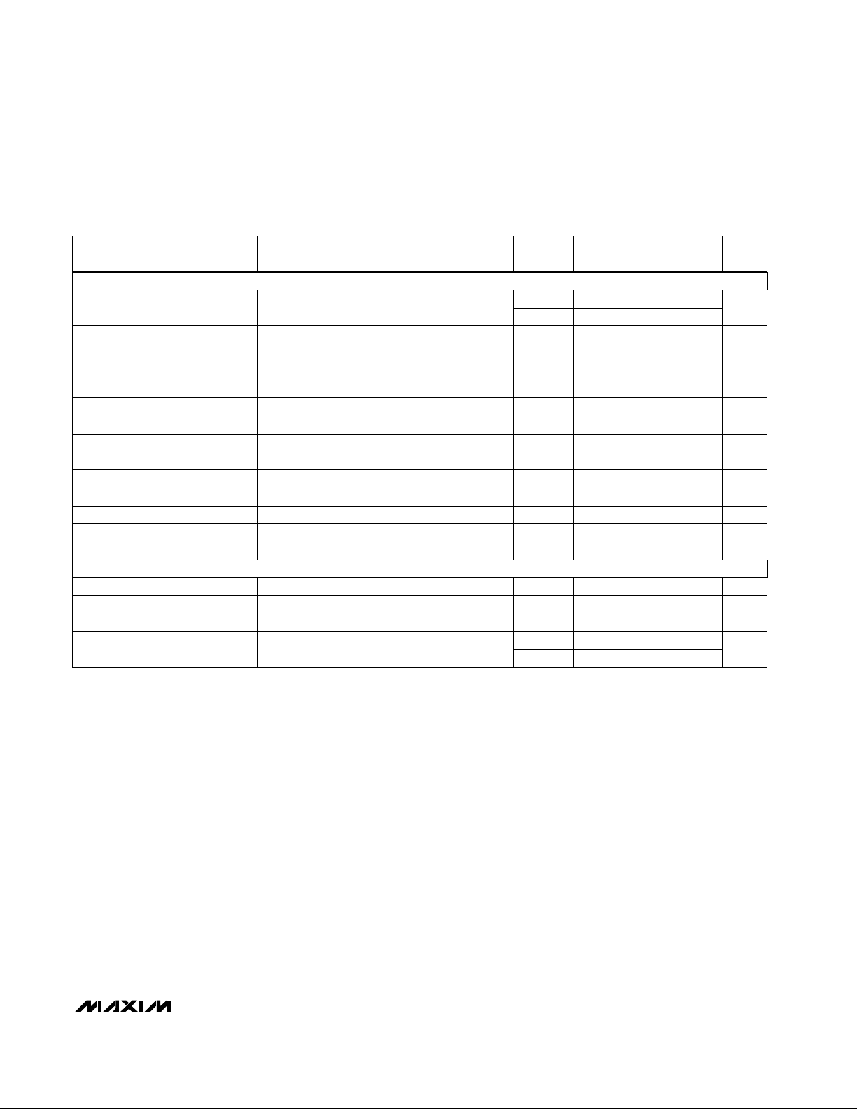
ELECTRICAL CHARACTERISTICS—Dual Supplies (continued)
(V+ = +4.5V to +5.5V, V- = -4.5V to -5.5V, V
INL
= 0.8V, V
INH
= 2.4V, V
GND
= 0V, TA= T
MIN
to T
MAX
, unless otherwise noted. Typical
values are at T
A
= +25°C.)
V
COM
= 0V, f = 1MHz, Figure 5 pF6C
COM(OFF)
COM_ Off Capacitance +25°C
-80
RL= 50Ω, V
COM
= 1V
RMS
,
f = 10MHz, Figure 4
dBV
ISO
Off Isolation (Note 7) +25°C
V+ = 5.5V, VIN= 0V or V+,
V- = -5.5V
SWITCH DYNAMIC CHARACTERISTICS
POWER SUPPLY

MAX4529
Low-Voltage, Bidirectional
RF/Video Switch
4 _______________________________________________________________________________________
CL= 1.0nF, VNC= 2.5V,
RS= 0Ω, Figure 3
V+ = 5V, V
COM
= 3V,
I
COM
= 1mA
V
COM
= 3V, V+ = 5V,
Figure 2
(Note 3)
V
COM
= 3V, V+ = 5V,
Figure 2
VIN= 0.8V or 2.4V
V+ = 5.5V; V
COM
= 1V, 4.5V
V+ = 5.5V, V
COM
= 1V,
VNC= 4.5V
V+ = 5.5V, V
COM
= 1V,
VNC= 4.5V
CONDITIONS
pC1.5 10QCharge Injection (Note 3)
ns
110
43 90
t
OFF
Turn-Off Time (Note 3)
ns
120
65 100
t
ON
Turn-On Time (Note 3)
µA-1 0.03 1I
INH
, I
INL
IN Input Current Logic High or
Low
V0.8 1.5V
INL
IN Input Logic Threshold Low
V1.5 2.4V
INH
IN Input Logic Threshold High
nA
-40 40
70 120
R
ON
Signal-Path On-Resistance
V0 V+V
COM
, V
NC
Analog Signal Range
-2 0.02 2
I
COM(ON)
COM On Leakage Current
(Notes 5, 6, 8)
nA
-20 20
-1 0.02 1
I
COM(OFF)
COM Off Leakage Current
(Notes 5, 6, 8)
nA
-20 20
Ω
150
-1 0.02 1
I
NC(OFF)
NC Off Leakage Current
(Notes 5, 6, 8)
UNITS
MIN TYP MAX
(Note 2)
SYMBOLPARAMETER
+25°C
+25°C
C, E
+25°C
+25°C
C, E
+25°C
C, E
+25°C
C, E
C, E
C, E
+25°C
C, E
C, E
+25°C
C, E
T
A
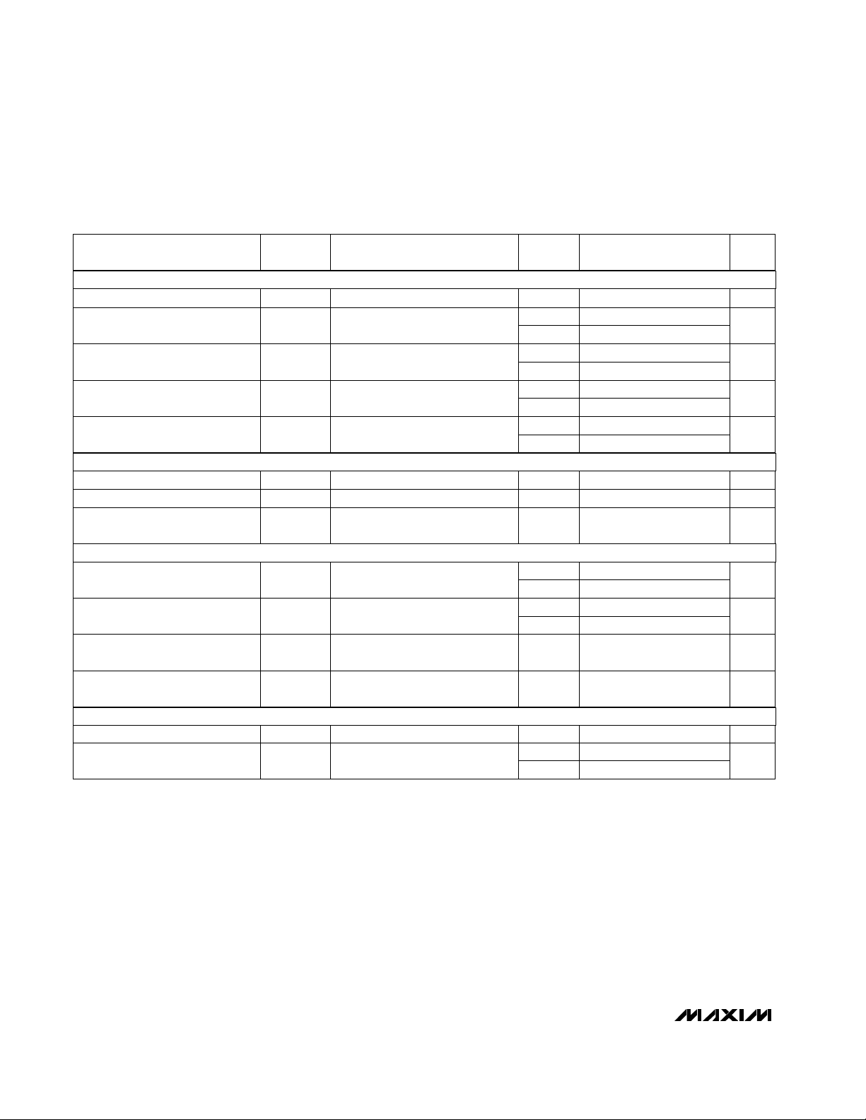
ELECTRICAL CHARACTERISTICS—Single +5V Supply
(V+ = +4.5V to +5.5V, V- = 0V, V
INL
= 0.8V, V
INH
= 2.4V, V
GND
= 0V, TA= T
MIN
to T
MAX
, unless otherwise noted. Typical values are
at T
A
= +25°C.)
V+ = 5.5V, VIN= 0V or V+
-1 0.05 1
I+V+ Supply Current µA
-10 10
+25°C
C, E
RL= 50Ω, V
COM
= 1V
RMS
,
f = 10MHz, Figure 4
dB-75V
ISO
Off-Isolation (Note 7) +25°C
V- = 0V 2.7 12.0V+Power-Supply Range VC, E
POWER SUPPLY
SWITCH DYNAMIC CHARACTERISTICS
LOGIC INPUT
ANALOG SWITCH
 Loading...