

For free samples & the latest literature: http://www.maxim-ic.com, or phone 1-800-998-8800.
For small orders, phone 408-737-7600 ext. 3468.
________________General Description
The MAX4528 low-voltage, CMOS analog IC is configured as a phase-reversal switch and optimized for highspeed applications such as chopper amplifiers. It
operates from a +2.7V to +12V single supply or from
±2.7V to ±6V dual supplies.
On-resistance (110Ω max) is matched between switches to 7Ω (max). Each switch can handle Rail-to-Rail
®
analog signals. The leakage current is only 0.5nA at
+25°C and 20nA at +85°C. All digital inputs have 0.8V
to 2.4V logic thresholds, ensuring both TTL- and
CMOS-logic compatibility.
For higher voltage operation, see the MAX4526/
MAX4527 data sheet.
________________________Applications
Chopper-Stabilized Amplifiers
Balanced Modulators/Demodulators
Data Acquisition
Test Equipment
Audio-Signal Routing
____________________________Features
♦ 5pC (max) Charge Injection
♦ 110Ω Signal Paths with ±5V Supplies
♦ Rail-to-Rail Signal Handling
♦ Transition Time <100ns with ±5V Supplies
♦ 1.0µA (max) Current Consumption
♦ >2kV ESD Protection per Method 3015.7
♦ TTL/CMOS-Compatible Input
♦ Small Packages: 8-Pin SO, DIP, and µMAX
MAX4528
Low-Voltage, Phase-Reversal
Analog Switch
________________________________________________________________
Maxim Integrated Products
1
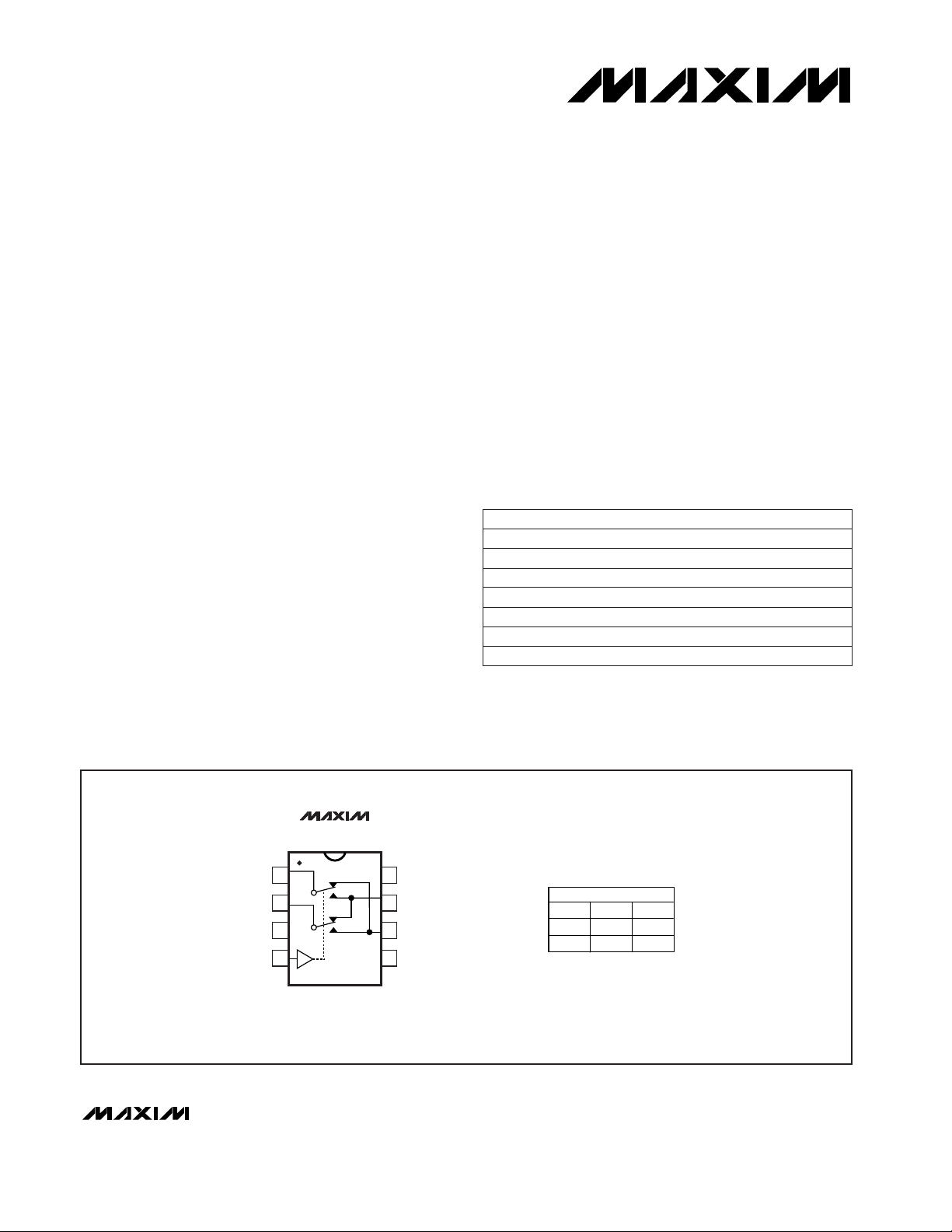
_________________________Pin Configuration/Functional Diagram/Truth Table
Y
SWITCH POSITIONS SHOWN WITH IN = LOW
V-
IN
1
2
8
7
V+
X
B
GND
A
MAX4528
DIP/SO/µMAX
TOP VIEW
3
4
6
5
TRUTH TABLE
IN
O
1
A
Y
X
B
X
Y
19-1325; Rev 0; 1/98
PART
MAX4528CPA
MAX4528CSA
MAX4528CUA 0°C to +70°C
0°C to +70°C
0°C to +70°C
TEMP. RANGE PIN-PACKAGE
8 Plastic DIP
8 SO
8 µMAX
_______________Ordering Information
*
Contact factory for availability.
MAX4528C/D
MAX4528EPA
MAX4528ESA -40°C to +85°C
-40°C to +85°C
0°C to +70°C Dice*
8 Plastic DIP
8 SO
MAX4528EUA -40°C to +85°C 8 µMAX
Rail-to-Rail is a registered trademark of Nippon Motorola Ltd.
MAX4528
Low-Voltage, Phase-Reversal
Analog Switch
2 _______________________________________________________________________________________
ABSOLUTE MAXIMUM RATINGS
ELECTRICAL CHARACTERISTICS: ±5V Dual Supplies
(V+ = 5V, V- = -5V, V
INH
= 2.4V, V
INL
= 0.8V, TA= T
MIN
to T
MAX
, unless otherwise noted. Typical values are at TA= +25°C.)
Stresses beyond those listed under “Absolute Maximum Ratings” may cause permanent damage to the device. These are stress ratings only, and functional
operation of the device at these or any other conditions beyond those indicated in the operational sections of the specifications is not implied. Exposure to
absolute maximum rating conditions for extended periods may affect device reliability.
(Voltages Referenced to GND)
V+ .............................................................................-0.3V to 13V
V-...............................................................................-13V to 0.3V
V+ to V-.....................................................................-0.3V to 13V
All Other Pins (Note 1)..........................(V- - 0.3V) to (V+ + 0.3V)
Continuous Current into Any Terminal..............................±20mA
Peak Current into Any Terminal
(pulsed at 1ms, 10% duty cycle)...................................±50mA
ESD per Method 3015.7 ..................................................>2000V
Continuous Power Dissipation (T
A
= +70°C) (Note 2)
Plastic DIP (derate 9.09mW/°C above +70°C) ............727mW
SO (derate 5.88mW/°C above +70°C).........................471mW
µMAX (derate 4.10mW/°C above +70°C) ....................330mW
Operating Temperature Ranges
MAX4528C_ _ .....................................................0°C to +70°C
MAX4528E_ _ ..................................................-40°C to +85°C
Storage Temperature Range.............................-65°C to +150°C
Lead Temperature (soldering, 10sec).............................+300°C
V
A
= VB= ±3V, IA= IB= 1mA
(Note 4)
CL= 1.0nF, VAor VB= 0V, Figure 5
VA= VB= ±3V, V+ = 5V, V- = -5V,
RL= 300Ω, Figure 4
VA= VB= ±3V, V+ = 5V, V- = -5V,
RL= 300Ω, Figure 3
RL= 50Ω, CL= 15pF, f = 1MHz,
VA= VB= 1V
RMS
, Figure 7
V
IN_
= 0.8V or 2.4V
VA= VB= GND, f = 1MHz, Figure 6
CONDITIONS
dB-68V
ISO
A-X, A-Y, B-X, B-Y Isolation
(Note 8)
pF13C
ON
A-X, A-Y, B-X, B-Y Capacitance
Ω
70 110
R
ON
A-X, A-Y, B-X, B-Y
On-Resistance
VV- V+
VA, VB,
VX, V
Y
Analog-Signal Range
pC1 5QCharge Injection (Note 4)
ns
1 20
t
BBM
Break-Before-Make Time Delay
ns
70 100
t
TRANS
Transition Time
V1.6 2.4V
INH
IN Input Logic Threshold High
V0.8 1.6V
INL
IN Input Logic Threshold Low
µA-1 0.03 1
I
INH
,
I
INL
IN Input Current Logic High
or Low
UNITS
MIN TYP MAX
(Note 3)
SYMBOLPARAMETER
Note 1: Signals on IN, A, B, X, or Y exceeding V+ or V- are clamped by internal diodes. Limit forward-diode current to maximum
current rating.
Note 2: All leads are soldered or welded to PC boards.
VA= VB= ±3V, IA= IB= 1mA Ω
3 7
∆R
ON
A-X, A-Y, B-X, B-Y
On-Resistance Match (Note 5)
VA= VB= 3V, 0V, -3V;
IA= IB= 1mA
Ω
9 15
R
FLAT(ON)
A-X, A-Y, B-X, B-Y
On-Resistance Flatness (Note 6)
V+ = 5.5V; V- = -5.5V; VIN= 0V, 3V;
VA= ±4.5V; VB= –+4.5V
nA
-0.5 0.01 0.5
IA, IB,
IX, I
Y
A-B, X-Y Leakage Current
(Note 7)
+25°C
+25°C
C, E
+25°C
+25°C
+25°C
+25°C
C, E
C, E
+25°C
C, E
+25°C
T
A
+25°C
C, E 130
C, E
C, E
C, E
9
17
-20 20
C, E
C, E
125
ANALOG SWITCH
LOGIC INPUT
SWITCH DYNAMIC CHARACTERISTICS
MAX4528
Low-Voltage, Phase-Reversal
Analog Switch
_______________________________________________________________________________________ 3
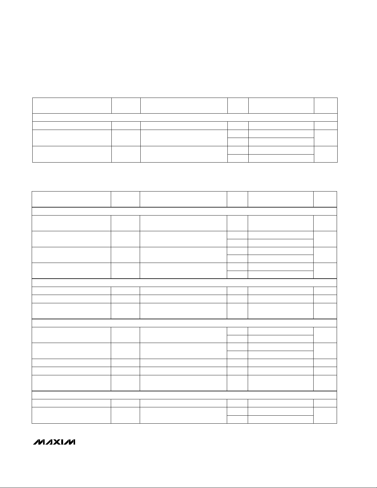
ELECTRICAL CHARACTERISTICS: +5V Single Supply
(V+ = 5V, V- = 0V, V
INH
= 2.4V, V
INL
= 0.8V, TA= T
MIN
to T
MAX
, unless otherwise noted. Typical values are at TA= +25°C.)
ELECTRICAL CHARACTERISTICS: ±5V Dual Supplies (continued)
(V+ = 5V, V- = -5V, V
INH
= 2.4V, V
INL
= 0.8V, TA= T
MIN
to T
MAX
, unless otherwise noted. Typical values are at TA= +25°C.)
CONDITIONS T
A
UNITS
MIN TYP MAX
(Note 3)
SYMBOLPARAMETER
C, E V±2.7 ±6V+, V-Power-Supply Range
VIN= 0V or V+
C, E
µA
-10 10
I+V+ Supply Current
+25°C -1 1
+25°C -1 1
VIN= 0V or V+
C, E
µA
-10 10
I-V- Supply Current
VA= VB= 3V, IA= IB= 1mA
(Note 4)
V+ = 5.5V; V
I
N
= 0V, 3V;
VA= 4.5V, 1V; VB= 1V, 4.5V
nA
-0.5 0.01 0.5
IA, IB,
IX, I
Y
CL= 1.0nF, VAor VB= 0V, Figure 5
VA= VB= 3V, V+ = 5V, RL= 300Ω,
Figure 4
+25°C
VA= VB= 3V, V+ = 5V, RL= 300Ω,
Figure 3
RL= 50Ω, CL= 15pF, f = 1MHz,
VA= VB= 1V
RMS
, Figure 7
V
IN_
= 0.8V or 2.4V
VA= VB= GND, f = 1MHz, Figure 6
CONDITIONS
A-B, X-Y Leakage Current
(Note 9)
C, E
+25°C
+25°C
+25°C
+25°C
C, E
C, E
+25°C
C, E
+25°C
T
A
+25°C
C, E 200
C, E
C, E
12
-20 20
C, E
C, E
200
dB-70V
ISO
A-X, A-Y, B-X, B-Y Isolation
(Note 8)
pF17C
OFF
A-X, A-Y, B-X, B-Y Capacitance
Ω
120 175
R
ON
A-X, A-Y, B-X, B-Y
On-Resistance
VV- V+
VA, VB,
VX, V
Y
Analog-Signal Range
pC1.5 5QCharge Injection
ns
1 20
t
BBM
Break-Before-Make Time Delay
ns
110 175
t
TRANS
Transition Time
V1.6 2.4V
INH
IN Input Logic Threshold High
V0.8 1.6V
INL
IN Input Logic Threshold Low
µA-1 0.03 1
I
INH
,
I
INL
IN Input Current Logic High
or Low
UNITS
MIN TYP MAX
(Note 3)
SYMBOLPARAMETER
VA= VB= 3V, IA= IB= 1mA Ω
5 10
∆R
ON
A-X, A-Y, B-X, B-Y
On-Resistance Match (Note 5)
C, E V2.7 12V+Power-Supply Range
+25°C -1 1
VIN= 0V or V+
C, E
µA
-10 10
I+V+ Supply Current
POWER SUPPLY
ANALOG SWITCH
LOGIC INPUT
SWITCH DYNAMIC CHARACTERISTICS (Note 4)
POWER SUPPLY
MAX4528
Low-Voltage, Phase-Reversal
Analog Switch
4 _______________________________________________________________________________________
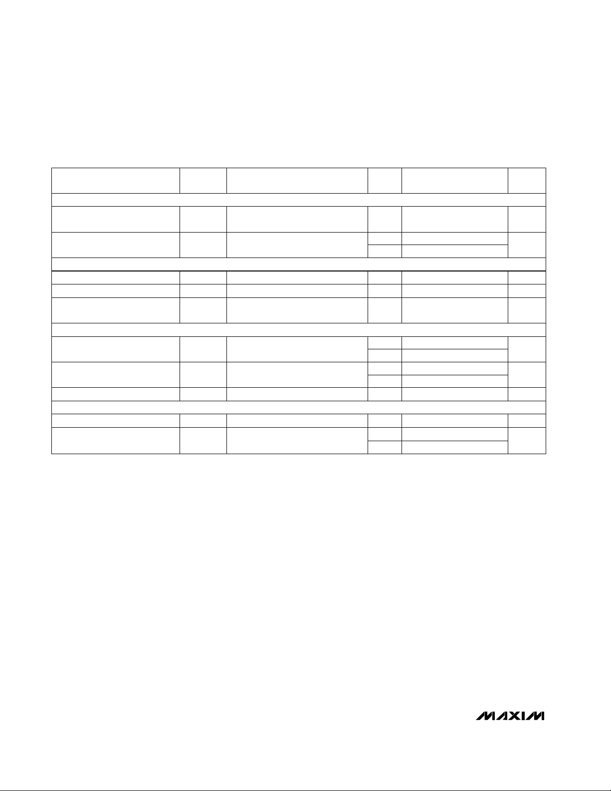
Note 3: The algebraic convention is used in this data sheet; the most negative value is shown in the minimum column.
Note 4: Guaranteed by design.
Note 5: ∆R
ON
= ∆R
ON(MAX)
- ∆R
ON(MIN)
.
Note 6: Resistance flatness is defined as the difference between the maximum and the minimum value of on-resistance as measured
over the specified analog-signal range.
Note 7: Leakage parameters are 100% tested at maximum rated hot temperature and guaranteed by correlation at +25°C.
Note 8: Off isolation = 20log
10
[(VXor VY) / (VAor VB)], VAor VB= output, VAor VB= input to off switch.
Note 9: Leakage testing for single-supply operation guaranteed by testing with dual supplies.
ELECTRICAL CHARACTERISTICS: +3V Single Supply
(V+ = 2.7V to 3.6V, V- = 0V, V
INH
= 2.4V, V
INL
= 0.6V, TA= T
MIN
to T
MAX
, unless otherwise noted. Typical values are at
T
A
= +25°C.)
V+ = 3V, VA= VB= 1.5V,
IA= IB= 0.1mA
(Note 4)
CL= 1.0nF, VAor VB= 0V, Figure 5
VA= 1.5V, VB= 0V, V+ = 3V,
V- = 0V, RL= 1kΩ, Figure 4
+25°C
VA= 1.5V, VB= 0V, V+ = 3V,
V- = 0V, RL= 1kΩ, Figure 3
V+ = 3V
V+ = 3V
V
IN_
= 0V or V+
CONDITIONS
C, E
+25°C
+25°C
+25°C
C, E
C, E
C, E
T
A
C, E 1000
C, E
C, E
C, E
500
V2.7 12V+, V-Power-Supply Range
+25°C -1 1
VIN= 0V or V+
C, E
µA
-10 10
I+V+ Supply Current
Ω
250 900
R
ON
A-X, A-Y, B-X, B-Y
On-Resistance
VV- V+
VA, VB,
VX, V
Y
Analog-Signal Range
pC1 5QCharge Injection
ns
2 150
t
BBM
Break-Before-Make Time Delay
ns
150 400
t
TRANS
Transition Time
V0.9 2.4V
INH
IN Input Logic Threshold High
V0.6 0.9V
INL
IN Input Logic Threshold Low
µA-1 0.03 1
I
INH
,
I
INL
IN Input Current Logic High
or Low
UNITS
MIN TYP MAX
(Note 3)
SYMBOLPARAMETER
ANALOG SWITCH
LOGIC INPUT
SWITCH DYNAMIC CHARACTERISTICS (Note 4)
POWER SUPPLY

MAX4528
Low-Voltage, Phase-Reversal
Analog Switch
_______________________________________________________________________________________
5
1000
10
-5 0-4 -3 -2 -1 1 2 3 4 5
ON-RESISTANCE vs. VA, V
B
(DUAL SUPPLIES)
MAX4528-01
VA, VB (V)
R
ON
(Ω)
100
V+ = 5V
V- = -5V
V+ = 1.2V
V- = -1.2V
V+ = 2V
V- = -2V
V+ = 2.7V
V- = -2.7V
V+ = 3.3V
V- = -3.3V
140
0
-5 2 5
100
MAX4528-02
VA, VB (V)
R
ON
(Ω)
-4 -3 -2 -1 0 1 3 4
80
60
120
20
40
ON-RESISTANCE vs.
V
A
, VB, AND TEMPERATURE
(DUAL SUPPLIES)
TA = +125°C
TA = +85°C
TA = +70°C
TA = -55°C
TA = +25°C
TA = -40°C
1000
10
0 1 2 3 4 5 6 7 8 9 10
100
MAX4528-03
V
A, VB
(V)
R
ON
(Ω)
ON-RESISTANCE vs. VA, VB
(SINGLE SUPPLY)
V- = 0V
V+ = 2V
V+ = 2.7V
V+ = 3.3V
V+ = 5V
V+ = 7.5V
V+ = 10V
200
0
0 5
140
MAX4528-04
VA, VB (V)
R
ON
(Ω)
1 2 3 4
120
80
100
180
160
20
40
60
ON-RESISTANCE vs.
V
A
, VB, AND TEMPERATURE
(SINGLE SUPPLY)
TA = -40°C
TA = -55°C
V+ = 5V
V- = 0V
TA = +25°C
TA = +125°C
TA = +70°C
TA = +85°C
4
-10
0 3 5
CHARGE INJECTION, CHARGE-
INJECTION MATCHING vs. V
A
, V
B
(+5V SUPPLY)
-6
-8
MAX4528-07
VA, VB (V)
Q (pC)
21
4
2
0
-2
-4
V+ = 5V
V- = 0V
Q
Y
Q
X
∆Q MATCHING
10,000
0.001
-55 -25 5 35 65 95 125
LEAKAGE vs. TEMPERATURE
0.01
MAX4528-05
TEMPERATURE (°C)
LEAKAGE (pA)
1
0.1
10
100
1000
10
-25
-5 -4 5
CHARGE INJECTION, CHARGE-
INJECTION MATCHING vs. V
A, VB
-20
5
MAX4528-06
V
A, VB
(V)
Q (pC)
-2 -1-3 20 1 3 4
0
-5
-10
-15
V+ = 5V
V- = 5V
∆Q MATCHING
Q
Y
Q
X
4
-3
0 3 5
CHARGE INJECTION, CHARGE-
INJECTION MATCHING vs. V
A
, V
B
(+3V SUPPLY)
-1
-2
MAX4528-08
VA, VB (V)
Q (pC)
21
4
3
2
1
0
V+ = 3V
V- = 0V
∆Q MATCHING
Q
X
Q
Y
250
200
150
50
100
0
MAX4528-09
SUPPLY VOLTAGE (V)
42
6
8 10
TRANSITION TIME
vs. SUPPLY VOLTAGE
t
TRANS
(ns)
SINGLE SUPPLY
DUAL SUPPLIES
__________________________________________Typical Operating Characteristics
(V+ = 5V, V- = -5V, GND = 0V, TA= +25°C, unless otherwise noted.)

MAX4528
Low-Voltage, Phase-Reversal
Analog Switch
6 _______________________________________________________________________________________
250
200
150
50
100
0
MAX4528-10
TEMPERATURE (°C)
TRANSITION TIME vs. TEMPERATURE
t
TRANS
(ns)
-55 -25 5 35 65 95 125
+2.7V SINGLE SUPPLY
±5V DUAL SUPPLIES
+5V SINGLE SUPPLY
1
10
-2
10
-1
10
-4
10
-3
10
-5
10
-9
10
-10
10
-8
10
-7
10
-6
10
-11
MAX4528-11
VIN (V)
0 1 2 3 4 5 6 789 10 11 12
SUPPLY CURRENT AND GROUND CURRENT
vs. INPUT VOLTAGE
I+, I
GND
(A)
V+ = 5V
V+ = 12V
V- = 0V
0
-120
0.1 10 1001 1000
FREQUENCY RESPONSE
-90
MAX4528-12
FREQUENCY (MHz)
LOSS (dB)
-60
-40
-20
-10
-100
-110
-80
-70
-50
-30
-150
-180
-60
PHASE (DEGREES)
30
90
150
180
-90
-120
-30
0
60
120
OFF ISOLATION
V+ = 5V
V- = -5V
50Ω IN AND OUT
ON LOSS
ON PHASE
100
0.01
10 100
TOTAL HARMONIC DISTORTION
vs. FREQUENCY
0.1
MAX4526/27 TOC-13
FREQUENCY (Hz)
THD (%)
1k 10k
20k
10
1
V+ = 5V
V- = -5V
600Ω IN AND OUT
3.0
2.5
2.0
1.0
0.5
1.5
0
MAX4528-14
V+ (V)
2 31 40 5 6 7 8 9 10 11 12
LOGIC-LEVEL THRESHOLD
vs. SUPPLY VOLTAGE
LOGIC-LEVEL THRESHOLD (V)
_________________________________Typical Operating Characteristics (continued)
(V+ = 5V, V- = -5V, GND = 0V, TA= +25°C, unless otherwise noted.)

MAX4528
Low-Voltage, Phase-Reversal
Analog Switch
_______________________________________________________________________________________ 7
_______________Detailed Description
The MAX4528 is a phase-reversal analog switch consisting of two normally open and two normally closed CMOS
analog switches arranged in a bridge configuration.
Analog signals are put into two input pins and taken out
of two output pins. A logic-level signal controls whether
the input signal is routed through normally or inverted. A
low-resistance DC path goes from inputs to outputs at all
times, yet isolation between the two signal paths is excellent. Analog signals range from V- to V+.
These parts are characterized and optimized with ±5V
supplies, and can operate from a single supply.
The MAX4528 is designed for DC and low-frequencysignal phase-reversal applications, such as chopper
amplifiers, modulator/demodulators, and self-zeroing or
self-calibrating circuits. Unlike conventional CMOS
switches externally wired in a bridge configuration,
both DC and AC symmetry are optimized with a small
8-pin configuration that allows simple board layout and
isolation of logic signals from analog signals.
Power-Supply Considerations
Overview
The MAX4528’s construction is typical of most CMOS
analog switches. It has three supply pins: V+, V-, and
GND. V+ and V- drive the internal CMOS switches and
set the analog-voltage limits on any switch. Reverse
ESD-protection diodes are internally connected
between each analog-signal pin and both V+ and V-.
One of these diodes conducts if any analog signal
exceeds V+ or V-.
Virtually all of the analog leakage current is through the
ESD diodes to V+ or V-. Although the ESD diodes on a
given signal pin are identical and therefore fairly well
balanced, they are reverse biased differently. Each is
biased by either V+ or V- and the analog signal. This
means their leakages vary as the signal varies. The
dif-
ference
in the two diode leakages from the signal path
to the V+ and V- pins constitutes the analog-signal-path
leakage current. All analog leakage current flows to the
supply terminals, not to the other switch terminal. This
explains how both sides of a given switch can show
leakage currents of either the same or opposite polarity.
There is no connection between the analog-signal
paths and GND. The analog-signal paths consist of an
N-channel and P-channel MOSFET with their sources
and drains paralleled and their gates driven out-ofphase to V+ and V- by the logic-level translators.
V+ and GND power the internal logic and logic-level
translator and set the input logic threshold. The logiclevel translator converts the logic levels to switched V+
and V- signals to drive the analog switches’ gates. This
drive signal is the only connection between GND and
the analog supplies. V+ and V- have ESD-protection
diodes to GND. The logic-level input has ESD protection to V+ and V-, but not to GND, so the logic signal
can go below GND (as low as V-) when bipolar supplies are used.
Increasing V- has no effect on the logic-level thresholds,
but it does increase the drive to the internal P-channel
switches, reducing overall switch on-resistance. V- also
sets the negative limit of the analog-signal voltage.
The logic-level input pin (IN) has ESD-protection diodes
to V+ and V- but not to GND, so it can be safely driven
to V+ and V-. The logic-level threshold (VIN) is CMOS/
TTL compatible when V+ is between 4.5V and 12V
(see
Typical Operating Characteristics
).
NAME FUNCTION
5 V-
Negative Analog Supply-Voltage
Input. Connect V- to GND for singlesupply operation.
PIN
1 A
Analog-Switch Input Terminal A.
Connected to Y when IN is low; connected to X when IN is high.
6 Y Analog-Switch Output Terminal Y
7 X Analog-Switch Output Terminal X
2 B
Analog-Switch Input Terminal B.
Connected to X when IN is low; connected to Y when IN is high.
8 V+
Positive Analog/Digital Supply-Voltage
Input. Internally connected to substrate.
4 IN
Logic-Level Control Inputs (see
Truth
Table
)
3 GND
Ground. Connect GND to digital
ground. (Analog signals have no
ground reference; they are limited to
V+ and V-.)
Note:
Pins A, B, X, and Y are identical and interchangeable.
Any may be considered as an input or output; signals pass
equally well in either direction. However, AC symmetry is best
when A and B are the inputs and X and Y are the outputs.
Reduce AC balance in critical applications by using A and X or
A and Y as the input, and B and X or B and Y as the output.
_____________________Pin Description

MAX4528
Low-Voltage, Phase-Reversal
Analog Switch
8 _______________________________________________________________________________________
Bipolar Supplies
The MAX4528 operates with bipolar supplies between
±2.7V and ±6.0V. The V+ and V- supplies need not be
symmetrical, but their sum cannot exceed the 13V
absolute maximum rating (see
Absolute Maximum
Ratings
).
Single Supply
The MAX4528 operates from a single +2.7V to +12V
supply when V- is connected to GND. Observe all of
the bipolar precautions when operating from a single
supply.
__________Applications Information
The MAX4528 is designed for DC and low-frequencysignal phase-reversal applications. Both DC and AC
symmetry are optimized for use with ±5V supplies.
Signal Phase/Polarity Reversal
The MAX4528 can reverse the phase or polarity of a
pair of signals that are out-of-phase and balanced to
ground. This is done by routing signals through the
MAX4528 and, under control of IN, reversing the two
signals paths inside the switch before sending out to a
balanced output. Figure 1 shows a typical example.
The MAX4528 cannot reverse the phase or polarity
of a single grounded signal, as can be done with an
inverting op amp or transformer.
Balanced Modulator/Demodulator
The MAX4528 can be used as a balanced modulator/
demodulator at carrier frequencies up to 100kHz
(Figure 2). Higher frequencies are possible, but as frequency increases, small imbalances in the MAX4528’s
internal capacitance and resistance gradually impair
performance. Similarly, imbalances in external circuit
capacitance and resistance to GND reduce overall carrier suppression.
The carrier is applied as a logic-level square wave to
IN. (Note that this voltage can go as negative as V-.)
For best carrier suppression, the power-supply voltages should be equal, the square wave should have a
precise 50% duty cycle, and both the input and output
signals should be symmetrical around ground. Bypass
V+ and V- to GND with 0.1µF ceramic capacitors, as
close to the IC pins as possible. In critical applications,
carrier suppression can be optimized by trimming duty
cycle, DC bias around GND, or external source and
load capacitance.
In signal lines, balancing both capacitance and resistance to GND produces the best carrier suppression.
Transformer coupling of input and output signals
provides the best isolation and carrier suppression.
Transformers can also provide signal filtering, impedance matching, or low-noise voltage gain. Use a
center-tapped transformer or high-resistance voltage
divider to provide a DC path to GND on either the input
or output signal. This ensures a DC path to GND and
symmetrical operation of the internal switches.
Y
IN
LOGIC LOW
GND
X
B
A
MAX4528 MAX4528
TRUTH TABLE
IN
O
1
A
Y
X
B
X
Y
V-
INPUTS
V+
V+
V-
OUTPUTS
Y
IN
LOGIC HIGH
X
B
A
GND V-
V-
INPUTS
V+
V+
OUTPUTS
Figure 1. Typical Application Circuits

MAX4528
Low-Voltage, Phase-Reversal
Analog Switch
_______________________________________________________________________________________ 9
50%
0V
V
IN
V
OUT
0V
V
B
V
A
V-
X
B
A +3V
-3V
V-
300Ω
GND
V- IS CONNECTED TO GND (0V) FOR SINGLE-SUPPLY OPERATION.
IN
V+
V
IN
50Ω
90%
90%
t
TRANS
t
TRANS
35pF
V+
V+
V
OUT
MAX4528
Figure 3. Address Transition Time
A
TIME WAVEFORMS
LOGIC
(CARRIER)
B
X
Y
X-Y
(OUTPUT)
OUTPUT SPECTRUM
FREQUENCY
AMPLITUDE
LOWER
SIDEBAND
UPPER
SIDEBAND
SUPPRESSED CARRIER
MODULATOR/DEMODULATOR CIRCUIT
LOGIC (CARRIER)
OUTPUT
IN
B
A
X
Y
GND
V-
V-
V+
V+
MAX4528
Figure 2. Balanced Modulator/Demodulator
______________________________________________Test Circuits/Timing Diagrams

MAX4528
Low-Voltage, Phase-Reversal
Analog Switch
10 ______________________________________________________________________________________
tF < 5ns
t
R
< 5ns
V-
X OR Y
B
A +3V
V-
300Ω
50Ω
GND
V- IS CONNECTED TO GND (0V) FOR SINGLE-SUPPLY OPERATION.
IN
V
IN
t
BBM
35pF
V+
V+
V
OUT
MAX4528
0V
0V
90%
50%
V
IN
V
OUT
V+
Figure 4. Break-Before-Make Interval
V-
X OR Y
A OR B
B OR A N.C.
V
A
OR V
B
∆V
OUT
V
OUT
V
IN
V+
0V
V-
GND
∆V
OUT
IS THE MEASURED VOLTAGE DUE TO CHARGE TRANSFER
ERROR Q WHEN THE CHANNEL TURNS OFF.
V- IS CONNECTED TO GND (0V) FOR SINGLE-SUPPLY OPERATION.
IN
V
IN
C
L
1000pF
50Ω
V+
V+
V
OUT
MAX4528
Q = ∆V
OUT
x C
L
Figure 5. Charge Injection
_________________________________Test Circuits/Timing Diagrams (continued)

MAX4528
Low-Voltage, Phase-Reversal
Analog Switch
______________________________________________________________________________________ 11
V-
Y
X
B
A
V-
GND
IN
V+
V+
MAX4528
SWITCH
SELECT
V+
1MHz
CAPACITANCE
ANALYZER
Figure 6. A, B, X, Y Capacitance
V-
X, Y
A, B
V-
GND
MEASUREMENTS ARE STANDARDIZED AGAINST SHORT AT SOCKET TERMINALS.
OFF ISOLATION IS MEASURED BETWEEN A, B AND "OFF" X, Y TERMINAL.
ON LOSS IS MEASURED BETWEEN A, B AND "ON" X, Y TERMINAL.
SIGNAL DIRECTION THROUGH SWITCH IS REVERSED; WORST VALUES ARE RECORDED.
V- IS CONNECTED TO GND (0V) FOR SINGLE-SUPPLY OPERATION.
V
OUT
V
IN
MEAS.
REF
50Ω
50Ω 50Ω
50Ω
IN
10nF
V+
10nF
V+
MAX4528
NETWORK
ANALYZER
OFF ISOLATION = 20log
V
OUT
V
IN
ON LOSS = 20log
V
OUT
V
IN
SWITCH
SELECT
V+
Figure 7. Off Isolation and On Loss
_________________________________Test Circuits/Timing Diagrams (continued)

8LUMAXD.EPS
MAX4528
Low-Voltage, Phase-Reversal
Analog Switch
Maxim cannot assume responsibility for use of any circuitry other than circuitry entirely embodied in a Maxim product. No circuit patent licenses are
implied. Maxim reserves the right to change the circuitry and specifications without notice at any time.
12
____________________Maxim Integrated Products, 120 San Gabriel Drive, Sunnyvale, CA 94086 408-737-7600
© 1998 Maxim Integrated Products Printed USA is a registered trademark of Maxim Integrated Products.
________________________________________________________Package Information
____________________________________________________________Chip Topography
TRANSISTOR COUNT: 141
SUBSTRATE IS INTERNALLY CONNECTED TO V+
0.054"
(1.37mm)
0.038
(0.97mm)
N
GND
B
V-
Y
X
V+
A
 Loading...