

Page 1
General Description
The MAX4524L/MAX4525L are low-voltage, single-supply CMOS analog switches configured as a 4-channel
multiplexer/demultiplexer (MAX4524L) and a doublepole/double-throw (DPDT) switch (MAX4525L). The
MAX4524L/MAX4525L have an inhibit input to simultaneously open all switches.
These devices operate from a single supply of +2V to
+12V. They are optimized for operation with a +12V supply. The on-resistance is 100Ω with a +12V supply. Each
switch can handle Rail-to-Rail analog signals. Off-leakage
current measures only 2nA at +25°C. All digital inputs
have 0.8V to 2.0V logic thresholds to ensure TTL/CMOSlogic compatibility when using a +12V supply.
Applications
Audio and Video Signal Routing
Data-Acquisition Systems
Communications Circuits
Automotive
DSL Modems
Features
♦ +3V Logic-Compatible Inputs
(VIH= 2.0V, VIL= 0.8V)
♦ +2V to +12V Supply Operation
♦ 100Ω On-Resistance with +12V Supply
♦ Guaranteed 10Ω On-Resistance Match at +12V
♦ Guaranteed 2nA Maximum Off-Leakage at +12V
♦ TTL/CMOS-Logic Compatible
♦ Tiny 10-Pin TDFN (3mm × 3mm) and 10-Pin µMAX
Packages
MAX4524L/MAX4525L
Low-Voltage, Single-Supply Analog
Multiplexers/Switches
________________________________________________________________ Maxim Integrated Products 1
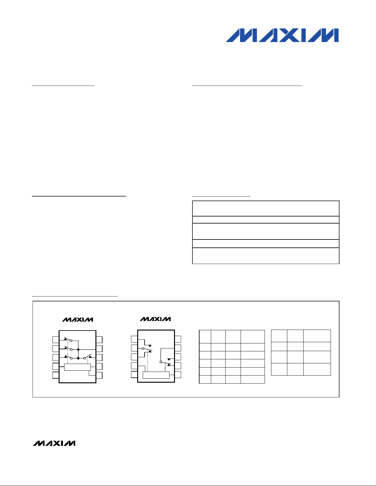
Pin Configurations/Functional Diagrams/Truth Tables
Ordering Information
1
2
3
4
5
10
9
8
7
6
V+
COM
NO0
ADDAINH
NO1
NO3
NO2
MAX4524L
µMAX/TDFN
TOP VIEW
ADDBGND
LOGIC
1
2
3
4
5
10
9
8
7
6
V+
COMB
NOB
NCBINH
NCA
COMA
NOA
MAX4525L
µMAX/TDFN
ADDGND
LOGIC
1
0
0
0
0
X
0
0
1
1
X
0
1
0
1
NONE
COM-NO0
COM-NO1
COM-NO2
COM-NO3
INH
MAX4524L
ADDB
ADDB
ADDA
ON
SWITCH
ON
SWITCH
INH
1
MAX4525L
X
00
01
NONE
COMA-NCA,
COMB-NCB
COMA-NOA,
COMB-NOB
19-2940; Rev 1; 6/07
For pricing delivery, and ordering information please contact Maxim Direct! at 1-888-629-4642,
or visit Maxim’s website at www.maxim-ic.com.
PART
TEMP RANGE
PINPACKAGE
TOP
MARK
MAX4524LEUB
10 µMAX —
MAX4524LETB
10 TDFN-EP*
(3mm x 3mm)
AAL
MAX4525LEUB
10 µMAX —
MAX4525LETB
10 TDFN-EP*
(3mm x 3mm)
AAM
*EP = Exposed pad.
-40°C to +85°C
-40°C to +85°C
-40°C to +85°C
-40°C to +85°C
Page 2
MAX4524L/MAX4525L
Low-Voltage, Single-Supply Analog
Multiplexers/Switches
2 _______________________________________________________________________________________
ABSOLUTE MAXIMUM RATINGS
ELECTRICAL CHARACTERISTICS—Single +12V Supply
(V+ = 12V ±5%, GND = 0V, VIH= 2.0V, VIL= 0.8V, TA= T
MIN
to T
MAX
, unless otherwise noted. Typical values are at TA = +25°C.)
(Notes 2, 3)
Stresses beyond those listed under “Absolute Maximum Ratings” may cause permanent damage to the device. These are stress ratings only, and functional
operation of the device at these or any other conditions beyond those indicated in the operational sections of the specifications is not implied. Exposure to
absolute maximum rating conditions for extended periods may affect device reliability.
(All Voltages Referenced to GND, Unless Otherwise Noted.)
V+ ...........................................................................-0.3V to +13V
Voltage at Any Pin (Note 1) ..........................-0.3V to (V+ + 0.3V)
Continuous Current into Any Terminal ..............................±20mA
Peak Current NO_, NC_ or COM_
(pulsed at 1ms, 10% duty cycle) ...................................±40mA
ESD per Method 3015.7 ..................................................>2000V
Continuous Power Dissipation (T
A
= +70°C)
10-Pin µMAX (derate 5.6mW/°C above +70°C) ...........444mW
10-Pin TDFN (derate 24.4mW/
o
C above +70°C) .......1951mW
Operating Temperature Range
MAX452_E_ _...................................................-40°C to +85°C
Storage Temperature Range .............................-65°C to +150°C
Junction Temperature......................................................+150°C
Lead Temperature (soldering, 10s) .................................+300°C
Note 1: Voltages exceeding V+ or GND on any signal terminal are clamped by internal diodes. Limit forward-diode current to maxi-
mum current rating.
PARAMETER
CONDITIONS TEMP
UNITS
ANALOG SWITCH
Analog Signal Range
0V+V
+25°C4580
COM-NO/NC
On-Resistance
R
ON
V+ = 11.4V, I
COM
= 1mA,
V
COM
= 10V
100
Ω
+25°C210
COM-NO/NC
On-Resistance
Match Between Channels
∆R
ON
V+ = 11.4V, I
COM
= 1mA,
V
COM
= 10V (Note 4)
15
Ω
COM-NO/NC OnResistance Flatness
R
FLAT
V+ = 11.4V, I
COM
= 1mA,
V
COM
= 1.5V, 6.0V, 10V
(Note 5)
+25°C512Ω
+25°C-2 +2
NO/NC Off-Leakage
I
NO(OFF)
I
NC(OFF)
V
COM
= 10V, 1.0V (Note 6)
-10
nA
+25°C-2 +2
-50
+25°C-2 +2
COM Off-Leakage
)
V+ = 12.6V,
V
NO
= 1V, 10V;
(Note 6)
-40°C to +85°C
-25
nA
+25°C-2 +2
-50
+25°C-2 +2
COM ON-Leakage
)
V+ = 12.6V,
(Note 6)
-25
nA
DIGITAL I/O (INH, ADD_)
Logic-Input Threshold High
V
IH
1.5 2.0 V
Logic-Input Threshold Low
V
IL
0.8 1.5 V
Input Current High I
IH
V
ADD_
= V
INH
= 2.0V +25°C-1 +1µA
Input Current Low I
IL
V
ADD_
= V
INH
= 0.8V +25°C-1 +1µA
SYMBOL
V
, V
C OM
N O__
MIN TYP MAX
-40°C to +85°C
-40°C to +85°C
I
COM(OFF
I
COM(ON
-40°C to +85°C
V+ = 12.6V, VNO = 1.0V, 10V,
-40°C to +85°C
+10
V
V
COM
COM
= 10V, 1V
= 10V, 1V
MAX4524L
-40°C to +85°C
+50
MAX4525L
MAX4524L
MAX4525L
-40°C to +85°C
-40°C to +85°C
+25
+50
+25
-40°C to +85°C
-40°C to +85°C
Page 3
MAX4524L/MAX4525L
Low-Voltage, Single-Supply Analog
Multiplexers/Switches
_______________________________________________________________________________________ 3
Note 2: The TDFN package is production tested at TA= +25°C. Limits over temperature are guaranteed by design.
Note 3: The algebraic convention used in this data sheet is where the most negative value is a minimum column.
Note 4: ∆R
ON
= R
ON(MAX)
- R
ON(MIN)
.
Note 5: Flatness is defined as the difference between the maximum and minimum value of on-resistance as measured over the
specified analog signal ranges.
Note 6: Leakage parameters are 100% tested at maximum-rated hot operating temperature and guaranteed by design at T
A
= +25°C.
Note 7: Guaranteed by design, not production tested.
PARAMETER
SYMBOL
CONDITIONS TEMP
MIN
TYP
MAX
UNITS
SWITCH DYNAMIC CHARACTERISTICS
+25°C 90 150
Inhibit Turn-On Time t
ON
VNO_= 10V, RL = 300Ω,
C
L
= 35pF, Figure 1
200
ns
+25°C 40 120
Inhibit Turn-Off Time t
OFF
VNO_= 10V, RL = 300Ω,
C
L
= 35pF, Figure 1
180
ns
+25°C 90 150
Address Transition Time t
TRANS
VNO_= 10V, RL = 300Ω,
C
L
= 35pF, Figure 2
200
ns
Break-Before-Make Time t
BBM
VNO = 10V, RL = 300Ω,
C
L
= 35pF, Figure 3
+25°C20ns
Charge Injection Q C = 1nF, Figure 4 (Note 7) +25°C 0.8 pC
NO/NC Off-Capacitance
)
+25°C4pF
+25°C14
COM Off-Capacitance
)
VNO_ = 0V, ƒ =
1MHz, Figure 5
+25°C6
pF
+25°C20
COM On-Capacitance
)
VNO_ = 0V, ƒ =
1MHz, Figure 5
+25°C12
pF
Off-Isolation V
ISO
+25°C92dB
Channel-to-Channel
Crosstalk (MAX4525L)
V
CT
+25°C96dB
On-Channel -3dB
Bandwidth
BW Figure 6 +25°C
MHz
Total Harmonic Distortion THD
R
L
= 600Ω, V
COM
= 2.5V
P-P,
20Hz to 20kHz BW
+25°C
%
POWER SUPPLY
Power-Supply Range V+
2
V
+25°C-1 +1
Power-Supply Current I+
V+ = 12.6V,
V
ADD_
= V
INH
= V+ or 0V
-10
µA
ELECTRICAL CHARACTERISTICS—Single +12V Supply (continued)
(V+ = 12V ±5%, GND = 0V, VIH= 2.0V, VIL= 0.8V, TA= T
MIN
to T
MAX
, unless otherwise noted. Typical values are at TA = +25°C.)
(Notes 2, 3)
C
NO(OFF
C
COM(OFF
C
COM(ON
VNO_ = 0V, ƒ = 1MHz, Figure 5
RL = 50Ω, ƒ = 1MHz, Figure 6
RL = 50Ω, ƒ = 1MHz, Figure 6
-40°C to +85°C
-40°C to +85°C
-40°C to +85°C
MAX4524L
MAX4525L
MAX4524L
MAX4525L
200
0.02
-40°C to +85°C
-40°C to +85°C
12.6
+10
Page 4
MAX4524L/MAX4525L
Low-Voltage, Single-Supply Analog
Multiplexers/Switches
4 _______________________________________________________________________________________
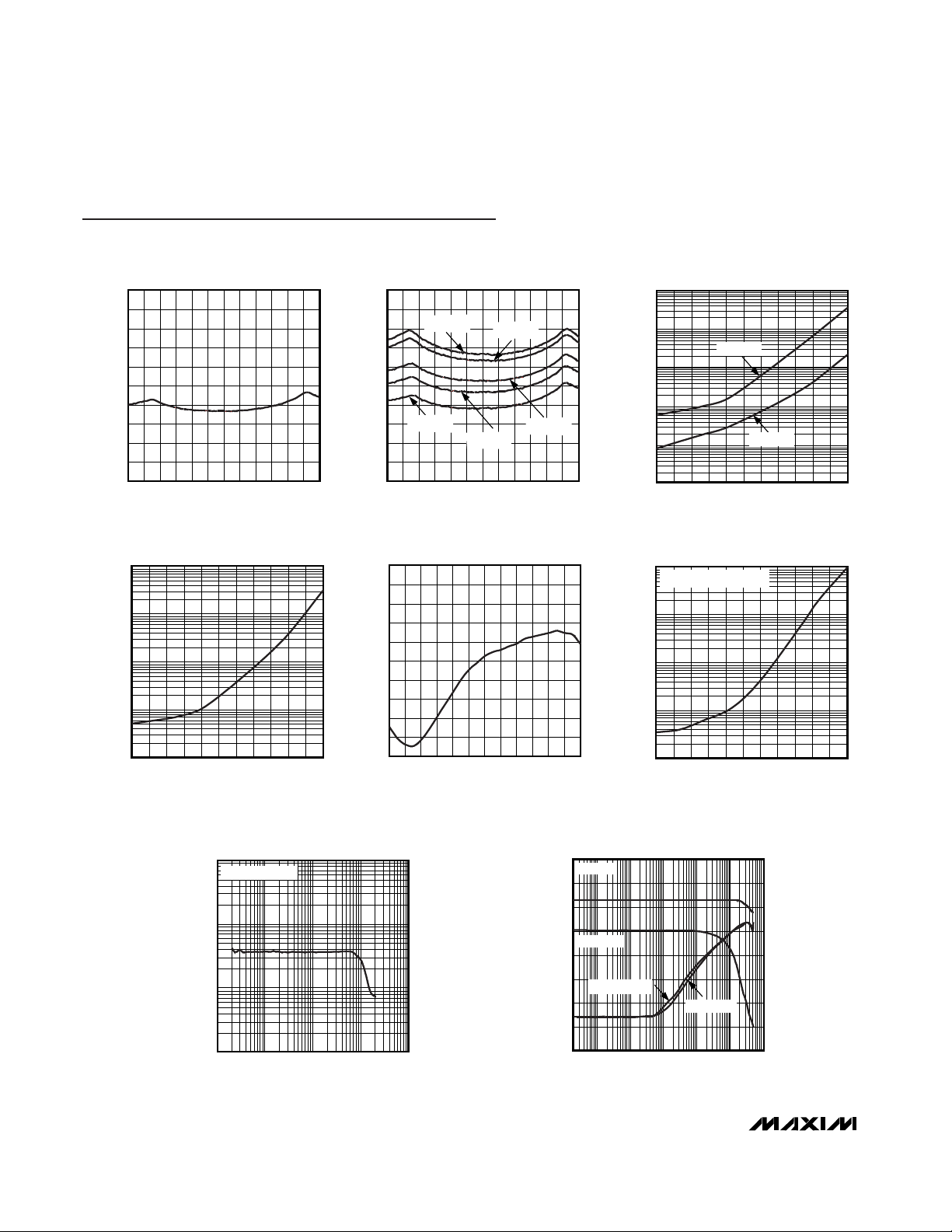
Typical Operating Characteristics
(V+ = 12V, V
INH
= GND, TA= +25°C, unless otherwise noted.)
0
20
10
50
40
30
60
70
90
80
100
0231 45678910 1211
ON-RESISTANCE vs. V
COM
MAX4524LTOC01
V
COM
(V)
ON-RESISTANCE (Ω)
0
14
7
35
28
21
42
49
63
56
70
ON-RESISTANCE vs. V
COM
MAX4524LTOC02
V
COM
(V)
ON-RESISTANCE (Ω)
0231 45678910 1211
TA = +25°C
TA = +70°C
TA = 0°C
TA = -40°C
T
A
= +85°C
100
-40 -10 20 50 80 110-25 5 35 65 95 125
10
1
0.1
0.01
0.001
OFF-LEAKAGE CURRENT
vs. TEMPERATURE
MAX4524L toc03
TEMPERATURE (°C)
OFF-LEAKAGE CURRENT (nA)
I
COM_OFF
I
NO_OFF
100
0.01
ON-LEAKAGE CURRENT
vs. TEMPERATURE
0.1
1
10
MAX4524Ltoc04
TEMPERATURE (°C)
ON-LEAKAGE CURRENT (nA)
-40 -10 20 50 80 110-25 5 35 65 95 125
0
2
1
5
4
3
6
7
9
8
10
CHARGE INJECTION vs. V
COM
MAX4524LTOC05
V
COM
(V)
CHARGE INJECTION (pC)
0231 45678910 1211
100
0.01
SUPPLY CURRENT vs. TEMPERATURE
0.1
1
10
MAX4524Ltoc06
TEMPERATURE (°C)
SUPPLY CURRENT (nA)
-40 -10 20 50 80 110-25 5 35 65 95 125
V
INH
= V
ADD_
= GND OR V+
10 100 1k 10k 100k
TOTAL HARMONIC DISTORTION
vs. FREQUENCY
MAX4524L toc07
FREQUENCY (Hz)
TOTAL HARMONIC DISTORTION (%)
0.1
0.01
0.0001
0.001
600Ω IN AND OUT
-130
-110
-90
-70
-50
-30
-10
10
30
FREQUENCY RESPONSE
FREQUENCY (MHz)
0.001 1 10 1000.01 0.1 1000
GAIN (dB)
-150
-120
-90
-60
-30
0
30
60
90
PHASE (DEGREES)
MAX4524L toc08
ON LOSS
CROSSTALK
OFF-ISOLATION
ON-PHASE
Page 5

MAX4524L/MAX4525L
Low-Voltage, Single-Supply Analog
Multiplexers/Switches
_______________________________________________________________________________________ 5
0624 81012
SUPPLY CURRENT
vs. LOGIC-LEVEL VOLTAGE
MAX4524L toc09
V
ADD_
, V
INH
(V)
SUPPLY CURRENT (µA)
0.0001
0.01
0.001
0.1
1
10
100
1000
10,000
Typical Operating Characteristics (continued)
(V+ = 12V, V
INH
= GND, TA= +25°C, unless otherwise noted.)
0
0.4
0.2
1.0
0.8
0.6
1.2
1.4
1.8
1.6
2.0
0231 45678910 1211
INPUT LOGIC THRESHOLD
vs. SUPPLY VOLTAGE
MAX4524LTOC10
SUPPLY VOLTAGE (V)
LOGIC THRESHOLD (V)
Pin Description
PIN
MAX4524L MAX4525L
NAME FUNCTION
1 — NO2 Analog Switch Normally Open Input 2
— 1 NOA Analog Switch A Normally Open Input
2 — NO3 Analog Switch Normally Open Input 3
— 2 COMA Analog Switch A Common
3 — NO1 Analog Switch Normally Open Input 1
— 3 NCA Analog Switch A Normally Closed Input
44INH
Inhibit. Drive INH low or connect to GND for normal operation. Drive INH high or
connect to V+ to turn all switches off.
5 5 GND
Ground. Connect to digital ground (analog signals have no ground reference,
but are limited to V+ and GND).
6 — ADDB Logic-Level Address Input (see Truth Tables)
— 6 ADD Logic-Level Address Input (see Truth Tables)
7 — ADDA Logic-Level Address Input (see Truth Tables)
— 7 NCB Analog Switch B Normally Closed Input
8 — NO0 Analog Switch Normally Open Input 0
— 8 NOB Analog Switch B Normally Open Input
9 — COM Analog Switch Common
— 9 COMB Analog Switch A Common
10 10 V+
Positive Analog and Digital Supply Voltage. Bypass with a 0.1µF capacitor to
GND.
EP EP
The bottom of the IC (TDFN package only) contains an exposed pad that must
be connected externally to V+.
Exposed PAD
Page 6

MAX4524L/MAX4525L
Detailed Description
The MAX4524L/MAX4525L are low-voltage, single-supply CMOS analog switches that operate from a single
supply of +2V to +12V. Operation with a +12V supply
optimizes the performance by reducing their on-resistance to 100Ω. The MAX4524L is configured as a 4channel multiplexer/demultiplexer and the MAX4525L is
a double-pole/double-throw (DPDT) switch. These
devices have an inhibit input (INH) to simultaneously
open all signal paths. Each switch can handle rail-torail analog signals. The off-leakage current is typically
only 0.1nA at +25°C and 10nA (max) over temperature.
All digital inputs have 0.8V to 2.0V logic-level thresholds, ensuring TTL/CMOS-logic compatibility when
using a single +12V supply.
Applications Information
Power-Supply Considerations
The MAX4524L/MAX4525Ls’ construction is typical of
most CMOS analog switches. The supply input, V+, is
used to power the internal CMOS switches and set the
limits of the analog voltage on any switch. Reverse ESD
protection diodes are internally connected between
each analog signal pin and both V+ and GND. If any
analog signal exceeds V+ or goes below GND, one of
these diodes conducts. During normal operation, these
reverse-biased ESD diodes leak, forming the only current drawn from V+ or GND. Virtually all the analog
leakage current comes from the ESD diodes. Although
the ESD diodes on a given signal pin are identical, and
therefore fairly well balanced, they are reverse biased
differently. Each is biased by either V+ or GND and the
analog signal. This means that leakage varies as the
signal varies. The difference in the two diode leakages
to the V+ and GND pins constitutes the analog signalpath leakage current. All analog leakage current flows
between each pin and one of the supply terminals, not
to the other switch terminal. This is why both sides of a
given switch can show leakage currents of either the
same or opposite polarity.
There is no connection between the analog signal
paths and GND. V+ and GND power the internal logic
and logic-level translators, and set both the input and
output logic limits. The logic-level translators convert
the logic levels into switched V+ and GND signals to
drive the gates of the analog signals. This drive signal
is the only connection between the logic supplies (and
signals) and the analog supplies.
Low-Voltage, Single-Supply Analog
Multiplexers/Switches
6 _______________________________________________________________________________________
Test Circuits/Timing Diagrams
50%
t
OFF
V+
0V
V
NO0
V
OUT
V
INH
0V
90%
90%
t
ON
50%
t
OFF
V+
0V
V
NO_
V
OUT
V
INH
0V
90%
90%
t
ON
V
INH
V
INH
V+
V
OUT
GND
V+
ADDB
ADDA
INH
NO0
NO1–NO3
COM
V+
MAX4524L
300Ω
50Ω
35pF
V+
V
OUT
GND
V+
ADD
INH
NO_
NC_
COM_
V+
MAX4525L
300Ω
35pF
50Ω
Figure 1. Inhibit Switching Times
Page 7

MAX4524L/MAX4525L
Low-Voltage, Single-Supply Analog
Multiplexers/Switches
_______________________________________________________________________________________ 7
_________________________________Test Circuits/Timing Diagrams (continued)
50%
t
TRANS
V+
0V
V
NO0
V
OUT
V
ADD
0V
90%
90%
t
TRANS
50%
t
TRANS
V+
0V
V
NC
V
OUT
V
ADD
0V
90%
90%
t
TRANS
V+
V
OUT
GND
V+
ADDB
ADDA
INH
NO0
NO1–NO2
NO3
COM
V+
MAX4524L
300Ω
50Ω
35pF
V+
V
OUT
GND
V+
ADD
V
ADD
INH
NO
NC
COM
V+
MAX4525L
300Ω
50Ω
35pF
Figure 2. Address Transition Time
Page 8

MAX4524L/MAX4525L
Low-Voltage, Single-Supply Analog
Multiplexers/Switches
8 _______________________________________________________________________________________
Test Circuits/Timing Diagrams (continued)
V+
V
OUT
V
OUT
V
ADD
V
ADD
GND
V+
ADDB
ADDA
INH
NO0–N03
COM
V+
MAX4524L
300Ω
50Ω
35pF
V+
GND
V+
ADD
INH
NO_, NC_
COM
V+
MAX4525L
300Ω
35pF
50Ω
50%
80%
t
BBM
tR < 20ns
t
F
< 20ns
V+
0V
V
COM
V
OUT
V
ADD
0V
Figure 3. Break-Before-Make Interval
0V
V+
V
INH
∆V
OUT
IS THE MEASURED VOLTAGE DUE TO CHARGE-
TRANSFER ERROR Q WHEN THE CHANNEL TURNS OFF.
∆V
OUT
Q = ∆V
OUT
× CL.
V
OUT
V+
V
OUT
VNO = 0V
CL = 1000pF
V
INH
GND
V+
ADDA
ADDB
INH
NO_
COM_
MAX4524L
MAX4525L
50Ω
Figure 4. Charge Injection
Page 9

MAX4524L/MAX4525L
Low-Voltage, Single-Supply Analog
Multiplexers/Switches
_______________________________________________________________________________________ 9
Chip Information
TRANSISTOR COUNT: 219
PROCESS: CMOS
Test Circuits/Timing Diagrams (continued)
V+
GND
V+
ADDB
ADDA
CHANNEL
SELECT
1MHz
CAPACITANCE
ANALYZER
INH
NO_
NO_
COM_
MAX4524L
MAX4525L
Figure 5. NO/COM Capacitance
MEASUREMENTS ARE STANDARDIZED AGAINST SHORT AT SOCKET TERMINALS.
OFF-ISOLATION IS MEASURED BETWEEN COM AND "OFF" NO TERMINAL ON EACH SWITCH.
ON-LOSS IS MEASURED BETWEEN COM AND "ON" NO TERMINAL ON EACH SWITCH.
CROSSTALK (MAX4524L) IS MEASURED FROM ONE CHANNEL (A, B) TO OTHER CHANNEL
SIGNAL DIRECTION THROUGH SWITCH IS REVERSED; WORST VALUES ARE RECORDED.
V+
V
OUT
V
IN
GND
V+
V
IN
V
OUT
MEAS.
NETWORK
ANALYZER
50Ω 50Ω
50Ω
OFF-ISOLATION = 20log ×
ON-LOSS = 20log ×
CROSSTALK = 20log ×
50Ω
REF.
ADDB
V
OUT
V
IN
V
OUT
V
IN
ADDA
CHANNEL
SELECT
INH
NO_
COM_
10nF
MAX4524L
MAX4525L
Figure 6. Off-Isolation, On-Loss, and Crosstalk
Page 10

MAX4524L/MAX4525L
Low-Voltage, Single-Supply Analog
Multiplexers/Switches
10 ______________________________________________________________________________________
Package Information
(The package drawing(s) in this data sheet may not reflect the most current specifications. For the latest package outline information
go to www.maxim-ic.com/packages
.)
10LUMAX.EPS
PACKAGE OUTLINE, 10L uMAX/uSOP
1
1
21-0061
REV.DOCUMENT CONTROL NO.APPROVAL
PROPRIETARY INFORMATION
TITLE:
TOP VIEW
FRONT VIEW
1
0.498 REF
0.0196 REF
S
6°
SIDE VIEW
α
BOTTOM VIEW
0° 0° 6°
0.037 REF
0.0078
MAX
0.006
0.043
0.118
0.120
0.199
0.0275
0.118
0.0106
0.120
0.0197 BSC
INCHES
1
10
L1
0.0035
0.007
e
c
b
0.187
0.0157
0.114
H
L
E2
DIM
0.116
0.114
0.116
0.002
D2
E1
A1
D1
MIN
-A
0.940 REF
0.500 BSC
0.090
0.177
4.75
2.89
0.40
0.200
0.270
5.05
0.70
3.00
MILLIMETERS
0.05
2.89
2.95
2.95
-
MIN
3.00
3.05
0.15
3.05
MAX
1.10
10
0.6±0.1
0.6±0.1
Ø0.50±0.1
H
4X S
e
D2
D1
b
A2
A
E2
E1
L
L1
c
α
GAGE PLANE
A2 0.030 0.037 0.75 0.95
A1
Page 11

MAX4524L/MAX4525L
Low-Voltage, Single-Supply Analog
Multiplexers/Switches
______________________________________________________________________________________ 11
Package Information (continued)
(The package drawing(s) in this data sheet may not reflect the most current specifications. For the latest package outline information
go to www.maxim-ic.com/packages
.)
6, 8, &10L, DFN THIN.EPS
Page 12

Revision History
Pages changed at Rev 1: 1, 5, 6, 11, 12
MAX4524L/MAX4525L
Low-Voltage, Single-Supply Analog
Multiplexers/Switches
Maxim cannot assume responsibility for use of any circuitry other than circuitry entirely embodied in a Maxim product. No circuit patent licenses are
implied. Maxim reserves the right to change the circuitry and specifications without notice at any time.
12 ____________________Maxim Integrated Products, 120 San Gabriel Drive, Sunnyvale, CA 94086 408-737-7600
© 2007 Maxim Integrated Products is a registered trademark of Maxim Integrated Products, Inc.
Package Information (continued)
(The package drawing(s) in this data sheet may not reflect the most current specifications. For the latest package outline information
go to www.maxim-ic.com/packages
.)
COMMON DIMENSIONS
SYMBOL MIN. MAX.
A 0.70 0.80
D 2.90 3.10
E 2.90 3.10
A1 0.00 0.05
L 0.20 0.40
PKG. CODE N D2 E2 e JEDEC SPEC b
[(N/2)-1] x e
PACKAGE VARIATIONS
0.25 MIN.k
A2 0.20 REF.
2.00 REF0.25±0.050.50 BSC2.30±0.1010T1033-1
2.40 REF0.20±0.05- - - - 0.40 BSC1.70±0.10 2.30±0.1014T1433-1
1.50±0.10 MO229 / WEED-3
0.40 BSC - - - - 0.20±0.05 2.40 REFT1433-2 14 2.30±0.101.70±0.10
T633-2 6 1.50±0.10 2.30±0.10 0.95 BSC MO229 / WEEA 0.40±0.05 1.90 REF
T833-2 8 1.50±0.10 2.30±0.10 0.65 BSC MO229 / WEEC 0.30±0.05 1.95 REF
T833-3 8 1.50±0.10 2.30±0.10 0.65 BSC MO229 / WEEC 0.30±0.05 1.95 REF
2.30±0.10 MO229 / WEED-3 2.00 REF0.25±0.050.50 BSC1.50±0.1010T1033-2
 Loading...