

Page 1
For free samples & the latest literature: http://www.maxim-ic.com, or phone 1-800-998-8800.
For small orders, phone 408-737-7600 ext. 3468.
________________General Description
The MAX4524/MAX4525 are low-voltage, single-supply
CMOS analog switches configured as a 4-channel multiplexer/demultiplexer (MAX4524) and a doublepole/double-throw (DPDT) switch (MAX4525). Both
have an inhibit input to simultaneously open all signal
paths.
These devices operate from a single supply of +2V to
+12V and are optimized for operation with +3V or +5V
supplies. On-resistance is 200Ω with a +5V supply and
500Ω with a +3V supply. Each switch can handle Railto-Rail®analog signals. The off-leakage current is only
2nA at +25°C or 20nA at +85°C.
All digital inputs have 0.8V to 2.4V logic thresholds,
ensuring TTL/CMOS-logic compatibility when using a
single +5V supply.
________________________Applications
Battery-Operated Equipment
Audio and Video Signal Routing
Low-Voltage Data-Acquisition Systems
Communications Circuits
____________________________Features
♦ Tiny 10-Pin µMAX Package
♦ Single-Supply Operation from +2V to +12V
♦ 200Ω On-Resistance with +5V Supply
♦ 500Ω On-Resistance with +3V Supply
♦ Guaranteed 8Ω On-Resistance Match at +5V
♦ Guaranteed 2nA Max On-Leakage at +5V
♦ TTL/CMOS-Logic Compatible
MAX4524/MAX4525
Low-Voltage, Single-Supply
Multiplexer and Switch
________________________________________________________________
Maxim Integrated Products
1
1
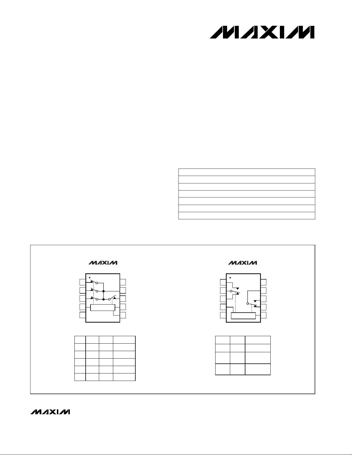
2
3
4
5
10
9
8
7
6
V+
COM
NO0
ADDAINH
NO1
NO3
NO2
MAX4524
µMAX
TOP VIEW
ADDBGND
INH
1
0
0
0
0
INH1ADD
X
00
01
ON SWITCH
NONE
COMA-NCA,
COMB-NCB
COMA-NOA,
COMB-NOB
ADDB
X
0
0
1
1
X = DON’T CARE
ADDA
X
0
1
0
1
ON SWITCH
NONE
COM-NO0
COM-NO1
COM-NO2
COM-NO3
LOGIC
1
2
3
4
5
10
9
8
7
6
V+
COMB
NOB
NCBINH
NCA
COMA
NOA
MAX4525
µMAX
ADDGND
LOGIC
______________________Pin Configurations/Functional Diagrams/Truth Tables
19-1332; Rev 0; 1/98
PART
MAX4524CUB
MAX4524C/D
MAX4524EUB -40°C to +85°C
0°C to +70°C
0°C to +70°C
TEMP. RANGE PIN-PACKAGE
10 µMAX
Dice*
10 µMAX
_______________Ordering Information
Rail-to-Rail is a registered trademark of Nippon Motorola Ltd.
MAX4525CUB
MAX4525C/D
MAX4525EUB -40°C to +85°C
0°C to +70°C
0°C to +70°C 10 µMAX
Dice*
10 µMAX
*
Contact factory for availability.
Page 2
MAX4524/MAX4525
Low-Voltage, Single-Supply
Multiplexer and Switch
2 _______________________________________________________________________________________
ABSOLUTE MAXIMUM RATINGS
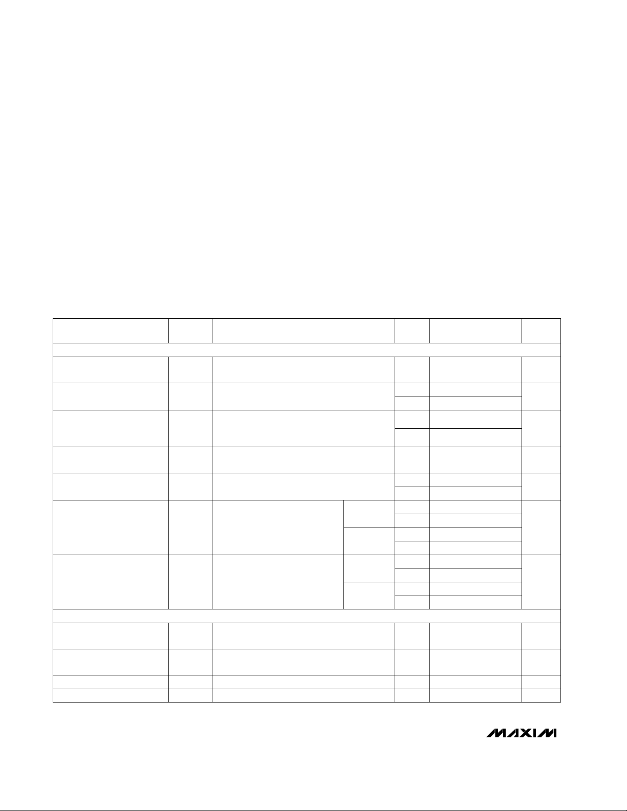
ELECTRICAL CHARACTERISTICS—Single +5V Supply
(V+ = +4.5V to +5.5V, GND = 0V, VAH= 2.4V, VAL= 0.8V, TA= T
MIN
to T
MAX
, unless otherwise noted. Typical values are at
T
A
= +25°C.)
Stresses beyond those listed under “Absolute Maximum Ratings” may cause permanent damage to the device. These are stress ratings only, and functional
operation of the device at these or any other conditions beyond those indicated in the operational sections of the specifications is not implied. Exposure to
absolute maximum rating conditions for extended periods may affect device reliability.
(Voltages Referenced to GND)
V+..............................................................................-0.3V, +13V
Voltage into any terminal (Note 1)................-0.3V to (V+ + 0.3V)
Continuous Current into any Terminal..............................±20mA
Peak Current, NO, NC or COM_
(pulsed at 1ms,10% duty cycle)....................................±40mA
ESD per Method 3015.7 ..................................................>2000V
Continuous Power Dissipation (T
A
= +70°C)
µMAX (derate 4.1mW/°C above +70°C) .......................330mW
Operating Temperature Ranges
MAX452_C_ _ ......................................................0°C to +70°C
MAX452_E_ _....................................................-40°C to +85°C
Storage Temperature Range.............................-65°C to +150°C
Lead Temperature (soldering, 10sec).............................+300°C
VA= V
INH
= 2.4V
V+ = 4.5V, I
COM
= 1mA, V
COM
= 3.5V
V+ = 5.5V; I
COM
= 1mA;
V
COM
= 1.5V, 2.5V, 3.5V
VA= V
INH
= 0.8V
CONDITIONS
µA-1 1I
IH
Input Current Low
90 150
VV- V+
V
COM
,
V
NO
Analog Signal Range
µA-1 1I
IH
Input Current High
Ω
2 10
∆R
ON
COM-NO/NC On-Resistance
Match Between Channels
(Note 3)
Ω5 12R
FLAT
COM-NO/NC On-Resistance
Flatness (Note 4)
-1 1
-2 2
UNITS
MIN TYP MAX
(Note 2)
SYMBOLPARAMETER
Note 1: Voltages exceeding V+ or GND on any signal terminal are clamped by internal diodes. Limit forward-diode current to max-
imum current rating.
V0.8 1.5V
IL
Logic Input Logic
Threshold Low
V+ = 5.5V; VNO= 1V, 4.5V; V
COM
= 4.5V, 1V nA
-10 10
I
NO(OFF),
I
NC(OFF),
NO/NC Off-Leakage
(Note 5)
+25°C
C, E
C, E
+25°C
+25°C
+25°C
+25°C
C, E
TEMP.
C, E
C, E
V+ = 4.5V, I
COM
= 1mA, V
COM
= 3.5V
C, E
Ω
200
R
ON
COM-NO/NC On-Resistance
C, E
-50 50C, E
V+ = 5.5V; VNO= 1V, 4.5V;
V
COM
= 4.5V, 1V
nA
-25 25
I
COM(OFF)
COM Off-Leakage
(Note 5)
C, E
-1 1+25°C
MAX4524
MAX4525
MAX4524
MAX4525
-50 50C, E
V+ = 5.5V; V
COM
= 4.5V, 1V nA
-25 25
I
COM(ON)
COM On-Leakage
(Note 5)
C, E
-1 1+25°C
-2 2+25°C
15
V1.5 2.4V
IH
Logic Input Logic
Threshold High
C, E
ANALOG SWITCH
DIGITAL I/O
Page 3
MAX4524/MAX4525
Low-Voltage, Single-Supply
Multiplexer and Switch
________________________________________________________________________________________ 3
ELECTRICAL CHARACTERISTICS—Single +5V Supply (continued)
(V+ = +4.5V to +5.5V, GND = 0V, VAH= 2.4V, VAL= 0.8V, TA= T
MIN
to T
MAX
, unless otherwise noted. Typical values are at
T
A
= +25°C.)
ELECTRICAL CHARACTERISTICS—Single +3V Supply
(V+ = +2.7V to +3.6V, GND = 0V, VAH= 2.0V, VAL= 0.5V, TA= T
MIN
to T
MAX
, unless otherwise noted. Typical values are at
T
A
= +25°C.)
RL = 600Ω, V
COM
= 2.5Vp-p, 20Hz to 20kHz
RL = 50Ω, f = 1MHz, Figure 5
RL= 50Ω, f = 1MHz, Figure 5
V
NO_
= 0V, f = 1MHz, Figure 6
C = 1nF, RS= 0Ω, VS= 2.5V, Figure 4
CONDITIONS
%0.2THDTotal Harmonic Distortion
-1 1
V2 12V+Power-Supply Range
V
NO_
= 3V, RL= 300Ω, CL= 35pF,
Figure 2
ns
200
t
(ON)
Inhibit Turn-On Time
+25°C
dB-74V
CT
Channel-to-Channel
Crosstalk (MAX4525)
dB-75V
ISO
Off-Isolation
20
14
pF4C
NO(OFF)
NO/NC Off-Capacitance
90 150
+25°C
pC0.8 5QCharge Injection (Note 6)
UNITS
MIN TYP MAX
(Note 2)
SYMBOLPARAMETER
+25°C
+25°C
+25°C
+25°C
+25°C
+25°C
TEMP.
+25°C
C, E
C, E
V
NO_
= 3V, RL= 300Ω, CL= 35pF,
Figure 2
ns
180
t
(OFF)
Inhibit Turn-Off Time
40 120+25°C
C, E
V
NO_
= 3V, RL= 300Ω, CL= 35pF, Figure 3 nst
BBM
Break-Before-Make Time
V
NO_
= 3V/0V, RL= 300Ω, CL= 35pF,
Figure 1
ns
200
t
TRANS
Address Transition Time
5 20+25°C
90 150+25°C
C, E
V+ = 5.5V, V
ADD
= V
INH
= V+ or 0V µA
-10 10
I+Power-Supply Current
C, E
V+ = 2.7V, I
COM
= 0.1mA, V
COM
= 1.5V
C, E
Ω
500
R
ON
COM-NO/NC On-Resistance
MAX4524
MAX4525
CONDITIONS
-50 50C, E
V+ = 3.6V; VNO= 1V, 3V;
V
COM
= 3V, 1V
nA
-25 25
I
COM(OFF)
COM Off-Leakage
(Note 6)
C, E
-1 1
V+ = 3.6V; VNO= 1V, 3V; V
COM
= 3V, 1V nA
-10 10
I
NO(OFF),
I
NC(OFF)
NO/NC Off-Leakage
(Note 6)
+25°C
C, E
+25°C
190 400
VV- V+
V
COM
,
V
NO
Analog Signal Range
-1 1
-2 2
UNITS
MIN TYP MAX
(Note 2)
SYMBOLPARAMETER
+25°C
+25°C
TEMP.
C, E
ANALOG SWITCH
V
NO_
= 0V, f = 1MHz, Figure 6 pF
6
C
COM(OFF)
COM Off-Capacitance
+25°C
V
NO_
= 0V, f = 1MHz, Figure 6 pF
12
C
COM(ON)
COM On-Capacitance
+25°C
SWITCH DYNAMIC CHARACTERISTICS
POWER SUPPLY
MAX4524
MAX4525
MAX4524
MAX4525
Page 4
MAX4524/MAX4525
Low-Voltage, Single-Supply
Multiplexer and Switch
4 _______________________________________________________________________________________
Note 2: The algebraic convention is used in this data sheet; the most negative value is shown in the minimum column.
Note 3: ∆R
ON
= R
ON(MAX)
- R
ON(MIN)
Note 4: Flatness is defined as the difference between the maximum and minimum value of on-resistance as measured over the
specified analog signal ranges; i.e., V
NO
= 3V to 0V and 0V to 3V.
Note 5: Leakage parameters are 100% tested at maximum-rated hot operating temperature, and guaranteed by correlation at
T
A
= +25°C.
Note 6: Guaranteed by design, not production tested.
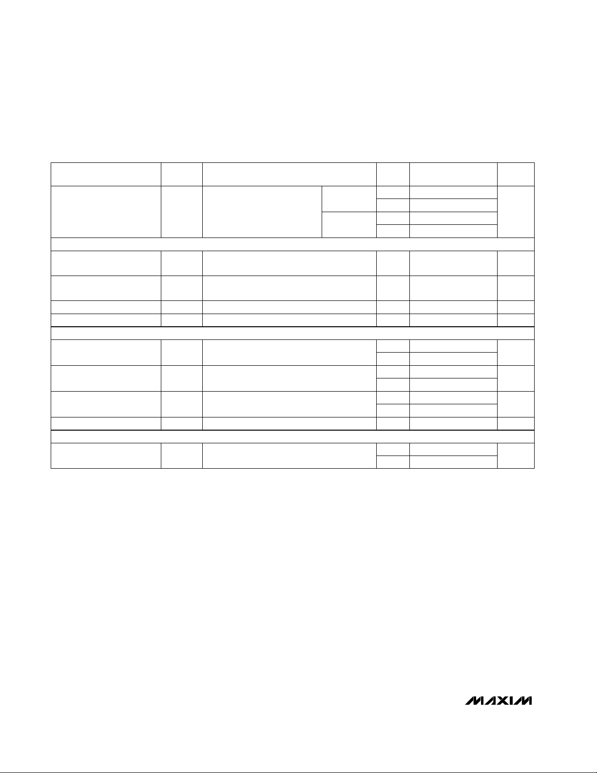
ELECTRICAL CHARACTERISTICS—Single +3V Supply (continued)
(V+ = +2.7V to +3.6V, GND = 0V, VAH= 2.0V, VAL= 0.5V, TA= T
MIN
to T
MAX
, unless otherwise noted. Typical values are at
T
A
= +25°C.)
VA= V
INH
= 2.0V
VA= V
INH
= 0.5V
CONDITIONS
+25°C
V1.0 2.0V
IH
Logic Input Logic
Threshold High
C, E
µA-1 1I
IH
Input Current Low
-2 2
µA-1 1I
IH
Input Current High
UNITS
MIN TYP MAX
(Note 2)
SYMBOLPARAMETER
V0.5 1.0V
IL
Logic Input Logic
Threshold Low
C, E
C, E
TEMP.
C, E
170 300+25°C
V
NO_
= 1.5V, RL= 300Ω, CL= 35pF,
Figure 2
50 200
ns
400
t
(ON)
Inhibit Turn-On Time
C, E
+25°C
V
NO_
= 1.5V, RL= 300Ω, CL= 35pF,
Figure 2
130 300
ns
300
t
(OFF)
Inhibit Turn-Off Time
C, E
+25°C
V
NO_
= 1.5V/0V, RL= 300Ω, CL= 35pF,
Figure 1
ns
400
t
TRANS
Address Transition Time
C, E
Figure 3, V
NO_
= 1.5V, RL= 300Ω, CL= 35pF ns5 40t
BBM
Break-Before-Make Time +25°C
-1 1+25°C
V+ = 3.6V, V
ADD
= V
INH
= V+ or 0V µA
-10 10
I+Power-Supply Current
C, E
C, E -50 50
V+ = 3.6V; V
COM
= 3V, 1V
C, EnA-25 25
I
COM(ON)
COM On-Leakage
(Note 6)
+25°C -1 1
MAX4524
MAX4525
DIGITAL I/O
SWITCH DYNAMIC CHARACTERISTICS (Note 6)
POWER SUPPLY
Page 5

MAX4524/MAX4525
Low-Voltage, Single-Supply
Multiplexer and Switch
_______________________________________________________________________________________
5
10,000
10
0 1 2 3 4 6 7 8 95 10
ON-RESISTANCE vs. V
COM
100
1000
MAX4524/25-01
V
COM
(V)
R
ON
(Ω)
V+ = 1.2V
V+ = 2V
V+ = 2.7V
V+ = 3.3V
V+ = 5V
V+ = 7.5V
V+ = 10V
130
10
0 1.0 3.0
ON-RESISTANCE vs. V
COM
AND TEMPERATURE
30
90
MAX4524/25-02
V
COM
(V)
R
ON
(Ω)
2.0 4.0
70
110
50
5..00.5 2.51.5 3.5 4.5
TA = +85°C
TA = -40°C
TA = 0°C
TA = +70°C
TA = +25°C
0.01
OFF-LEAKAGE vs.
TEMPERATURE
100
MAX4524/25-03
TEMPERATURE (°C)
OFF-LEAKAGE (nA)
1
0.1
10
-50 12525-25 0 7550 100
V+ = 5.5V
COM OFF
NO OFF
1
ON-LEAKAGE vs.
TEMPERATURE
10,000
100,000
MAX4524/25-04
TEMPERATURE (°C)
ON-LEAKAGE (pA)
100
10
1000
-50 12525-25 0 7550 100
V+ = 5.5V
100
0.01
10 1k 10k100 100k
TOTAL HARMONIC DISTORTION
vs. FREQUENCY
0.1
MAX4524/25-07
FREQUENCY (Hz)
THD (%)
1
10
600Ω IN AND OUT
0 1 3
CHARGE INJECTION vs. V
COM
-2.5
1.5
1.0
0.5
0
MAX4524/25-05
V
COM
(V)
Q (pC)
2 4
-0.5
-1.0
-1.5
-2.0
5
V+ = +5V
V- = 0V
1
SUPPLY CURRENT vs.
TEMPERATURE
100
MAX4524/25-06
TEMPERATURE (°C)
I+, (nA)
10
-50 12525-25 0 7550 100
V+ = 5V
V
INH
= VA = 0V, 5V
I+
0
-120
0.1 10 1001 300
FREQUENCY RESPONSE
-90
-100
-110
MAX4524/25-08
FREQUENCY (MHz)
LOSS (dB)
-70
-80
-50
-60
-20
-30
-40
-10
120
-120
-60
-80
-100
PHASE (DEGREES)
-20
-40
20
0
80
60
40
100
ON LOSS
50Ω IN AND OUT
OFF LOSS
ON PHASE
__________________________________________Typical Operating Characteristics
(V+ = +5V, GND = 0V, TA = +25°C, unless otherwise noted.)
Page 6

MAX4524/MAX4525
Low-Voltage, Single-Supply
Multiplexer and Switch
6 _______________________________________________________________________________________
0
0.5
1.5
1.0
2.0
2.5
3.0
0 32 41 5 6 7 8 10 119 12
LOGIC-LEVEL THRESHOLD vs. V+
MAX4524/25-10
V+ (V)
V
INH
, V
ADD_
(V)
______________________________________________________________ Pin Description
MAX4524
Analog Switch Normally Open Input 2—1
FUNCTIONMAX4525
NO2
NAME
NOA Analog Switch “A” Normally Open Input1—
NO3
COMA Analog Switch “A” Common2—
Analog Switch Normally Open Input 3—2
NO1
NCA Analog Switch “A” Normally Closed Input3—
INH
GND
Ground. Connect to digital ground (analog signals have no ground reference, but
are limited to V+ and GND).
55
Inhibit. Connect to GND for normal operation. Connect to logic-level high to turn all
switches off.
44
Analog Switch Normally Open Input 1—3
ADDB
ADD Logic-Level Address Input (see
Truth Tables
)6—
ADDA
NCB Analog Switch “B” Normally Closed Input7—
Logic-Level Address Input (see
Truth Tables
)—7
Logic-Level Address Input (see
Truth Tables
)—6
NO0 Analog Switch Normally Open Input 0—8
NOB
COM Analog Switch Common—9
Analog Switch “B” Normally Open Input8—
COMB
V+ Positive Analog and Digital Supply-Voltage Input1010
Analog Switch “A” Common9—
Note: NO_, NC_, and COM_ analog signal pins are identical and interchangeable. Any may be considered an input or output;
signals pass equally well in both directions.
10
-11
10
-9
10
-10
10
-6
10
-7
10
-8
10
-5
10
-4
10
-1
10
-2
10
-3
1
0 2 31 4 5 6 7 8 9 101112
V+ CURRENT vs. LOGIC LEVEL
MAX4524/25-09
V
ADD_
, V
INH
(V)
I+ CURRENT
V+ = +12V
V+ = +5V
Typical Operating Characteristics (continued)
(V+ = +5V, GND = 0V, TA= +25°C, unless otherwise noted.)
Page 7

__________Applications Information
Power-Supply Considerations
The MAX4524/MAX4525’s construction is typical of
most CMOS analog switches. They have two supply
pins: V+ and GND. V+ and GND are used to drive the
internal CMOS switches and set the limits of the analog
voltage on any switch. Reverse ESD-protection diodes
are internally connected between each analog signal
pin and both V+ and GND. If any analog signal
exceeds V+ or GND, one of these diodes will conduct.
During normal operation, these (and other) reversebiased ESD diodes leak, forming the only current drawn
from V+ or GND.
Virtually all the analog leakage current comes from the
ESD diodes. Although the ESD diodes on a given signal pin are identical, and therefore fairly well balanced,
they are reverse-biased differently. Each is biased by
either V+ or GND and the analog signal. This means
that leakage will vary as the signal varies. The difference in the two diode leakages to the V+ and GND
pins constitutes the analog signal-path leakage current.
All analog leakage current flows between each pin and
one of the supply terminals, not to the other switch terminal. This is why both sides of a given switch can
show leakage currents of either the same or opposite
polarity.
MAX4524/MAX4525
Low-Voltage, Single-Supply
Multiplexer and Switch
_______________________________________________________________________________________ 7
______________________________________________Test Circuits/Timing Diagrams
50%
t
TRANS
V+
0V
V
NO0
V
OUT
V
ADD
0V
90%
90%
t
TRANS
50%
t
TRANS
V+
0V
V
NC
V
OUT
V
ADD
0V
90%
90%
t
TRANS
V
ADD
V+
V
OUT
GND
V+
ADDB
ADDA
INH
NO0
NO1–NO2
NO3
COM
V+
MAX4524
300Ω
50Ω
35pF
V+
V
OUT
GND
V+
ADD
V
ADD
INH
NO
NC
COM
V+
MAX4525
300Ω
50Ω
35pF
REPEAT TEST FOR EACH SECTION.
Figure 1. Address Transition Time
Page 8

MAX4524/MAX4525
There is no connection between the analog signal
paths and GND. V+ and GND power the internal logic
and logic-level translators, and set both the input and
output logic limits. The logic-level translators convert
the logic levels into switched V+ and GND signals to
drive the gates of the analog signals. This drive signal
is the only connection between the logic supplies (and
signals) and the analog supplies. V+ has an ESD-protection diode to GND.
Low-Voltage Operation
These devices operate from a single supply between
+2V and +12V. At room temperature, they actually
“work” with a single supply at near or below +1.7V,
although as supply voltage decreases, switch on-resistance and switching times become very high.
High-Frequency Performance
In 50Ω systems, signal response is reasonably flat up
to 50MHz (see
Typical Operating Characteristics
).
Above 20MHz, the on-response has several minor
peaks, which are highly layout dependent. The problem
is not turning the switch on, but turning it off. The offstate switch acts like a capacitor, and passes higher
frequencies with less attenuation. At 10MHz, off-isolation is about -50dB in 50Ω systems, becoming worse
(approximately 20dB per decade) as frequency
increases. Higher circuit impedances also degrade offisolation. Adjacent channel attenuation is about 3dB
above that of a bare IC socket, and is entirely due to
capacitive coupling.
Low-Voltage, Single-Supply
Multiplexer and Switch
8 _______________________________________________________________________________________
_________________________________Test Circuits/Timing Diagrams (continued)
50%
t
OFF
V+
0V
V
NO0
V
OUT
V
INH
0V
90%
90%
t
ON
50%
t
OFF
V+
0V
V
NO_
V
OUT
V
INH
0V
90%
90%
t
ON
V
INH
V
INH
V+
V
OUT
GND
V+
ADDB
ADDA
INH
NO0
NO1–NO3
COM
V+
MAX4524
300Ω
50Ω
35pF
V+
V
OUT
GND
V+
ADD
INH
NO_
NC_
COM_
V+
MAX4525
300Ω
35pF
50Ω
REPEAT TEST FOR EACH SECTION.
Figure 2. Inhibit Switching Times
Page 9

MAX4524/MAX4525
Low-Voltage, Single-Supply
Multiplexer and Switch
_______________________________________________________________________________________ 9
50%
V+
0V
V
COM
V
OUT
V
ADD
0V
80%
t
BBM
V+
V
OUT
V
OUT
V
ADD
V
ADD
GND
V+
ADDB
ADDA
INH
NO0–N03
COM
V+
MAX4524
300Ω
50Ω
35pF
V+
GND
V+
ADD
INH
NO_, NC_
COM_
V+
MAX4525
300Ω
35pF
50Ω
REPEAT TEST FOR EACH SECTION.
t
R
< 20ns
t
F
< 20ns
Figure 3. Break-Before-Make Interval
0V
V+
V
INH
∆ V
OUT
IS THE MEASURED VOLTAGE DUE TO CHARGE-
TRANSFER ERROR Q WHEN THE CHANNEL TURNS OFF.
∆ V
OUT
REPEAT TEST FOR EACH SECTION.
Q = ∆ V
OUT
X C
L
V
OUT
V+
V
OUT
VNO = 0V
V
INH
GND
V+
ADDB
CHANNEL
SELECT
ADDA
INH
NO_
COM_
MAX4524
MAX4525
50Ω
CL
1000pF
_________________________________Test Circuits/Timing Diagrams (continued)
Figure 4. Charge Injection
Page 10

MAX4524/MAX4525
Low-Voltage, Single-Supply
Multiplexer and Switch
10 ______________________________________________________________________________________
_________________________________Test Circuits/Timing Diagrams (continued)
MEASUREMENTS ARE STANDARDIZED AGAINST SHORT AT SOCKET TERMINALS.
OFF-ISOLATION IS MEASURED BETWEEN COM AND "OFF" NO TERMINAL ON EACH SWITCH.
ON-LOSS IS MEASURED BETWEEN COM AND "ON" NO TERMINAL ON EACH SWITCH.
CROSSTALK (MAX4524) IS MEASURED FROM ONE CHANNEL (A, B) TO OTHER CHANNEL.
SIGNAL DIRECTION THROUGH SWITCH IS REVERSED; WORST VALUES ARE RECORDED.
V+
V
OUT
V
IN
GND
V+
V
IN
V
OUT
MEAS.
NETWORK
ANALYZER
50Ω 50Ω
50Ω
OFF ISOLATION = 20log
ON LOSS = 20log
CROSSTALK = 20log
50Ω
REF.
ADDB
V
OUT
V
IN
V
OUT
V
IN
ADDA
CHANNEL
SELECT
INH
NO_
COM_
10nF
MAX4524
MAX4525
Figure 5. Off-Isolation, On-Loss, and Crosstalk
V+
GND
V+
ADDB
ADDA
CHANNEL
SELECT
1MHz
CAPACITANCE
ANALYZER
INH
NO_
NO_
COM_
MAX4524
MAX4525
Figure 6. NO/COM Capacitance
Page 11

MAX4524/MAX4525
Low-Voltage, Single-Supply
Multiplexer and Switch
______________________________________________________________________________________ 11
__________________________________________________________Chip Topographies
TRANSISTOR COUNT: 219
SUBSTRATE CONNECTED TO V+
MAX4524 MAX4525
N.C.
COM
N.C.
NO0
ADDA
NO2
N.C. V+ N.C.
0.069"
(1.75mm)
0.053"
(1.35mm)
N.C.
GND
N.C.
ADDB
N.C.
NO3
NO1
INH
N.C.
COMB
NOB
NCB
N.C.
N.C.
N.C. V+ N.C.
0.069"
(1.75mm)
0.053"
(1.35mm)
N.C.
GND
N.C.
ADD
NOA
COMA
NCA
INH
N.C. = No Connection
Page 12

MAX4524/MAX4525
Low-Voltage, Single-Supply
Multiplexer and Switch
Maxim cannot assume responsibility for use of any circuitry other than circuitry entirely embodied in a Maxim product. No circuit patent licenses are
implied. Maxim reserves the right to change the circuitry and specifications without notice at any time.
12
____________________Maxim Integrated Products, 120 San Gabriel Drive, Sunnyvale, CA 94086 408-737-7600
© 1998 Maxim Integrated Products Printed USA is a registered trademark of Maxim Integrated Products.
________________________________________________________Package Information
10LUMAXB.EPS
 Loading...