

_______________General Description
The MAX4521/MAX4522/MAX4523 are quad, low-voltage, single-pole/single-throw (SPST) analog switches.
On-resistance (100Ω max) is matched between switches to 4Ω max, and is flat (12Ω max) over the specified
signal range. Each switch can handle rail-to-rail analog
signals. The off-leakage current is only 1nA at +25°C
and 10nA at +85°C.
The MAX4521 has four normally closed (NC) switches,
and the MAX4522 has four normally open (NO) switches. The MAX4523 has two NC switches and two NO
switches.
These CMOS switches can operate with dual power
supplies ranging from ±2V to ±6V or a single supply
between +2V and +12V. They are fully specified for single +2.7V operation.
All digital inputs have +0.8V and +2.4V logic thresholds, ensuring TTL/CMOS-logic compatibility when
using ±5V or a single +5V supply.
________________________Applications
Battery-Operated Equipment
Data Acquisition
Test Equipment
Avionics
Audio Signal Routing
Networking
____________________________Features
♦ +2V to +12V Single Supply
±2V to ±6V Dual Supplies
♦ 100Ω Signal Paths with ±5V Supplies
♦ Low Power Consumption, <1µW
♦ 4 Separately Controlled SPST Switches
♦ Rail-to-Rail Signal Handling
♦ Pin Compatible with Industry-Standard
DG211/DG212/DG213
♦ >2kV ESD Protection per Method 3015.7
♦ TTL/CMOS-Compatible Inputs with ±5V or
Single +5V Supply
MAX4521/MAX4522/MAX4523
Quad, Low-Voltage, SPST Analog Switches
________________________________________________________________
Maxim Integrated Products
1
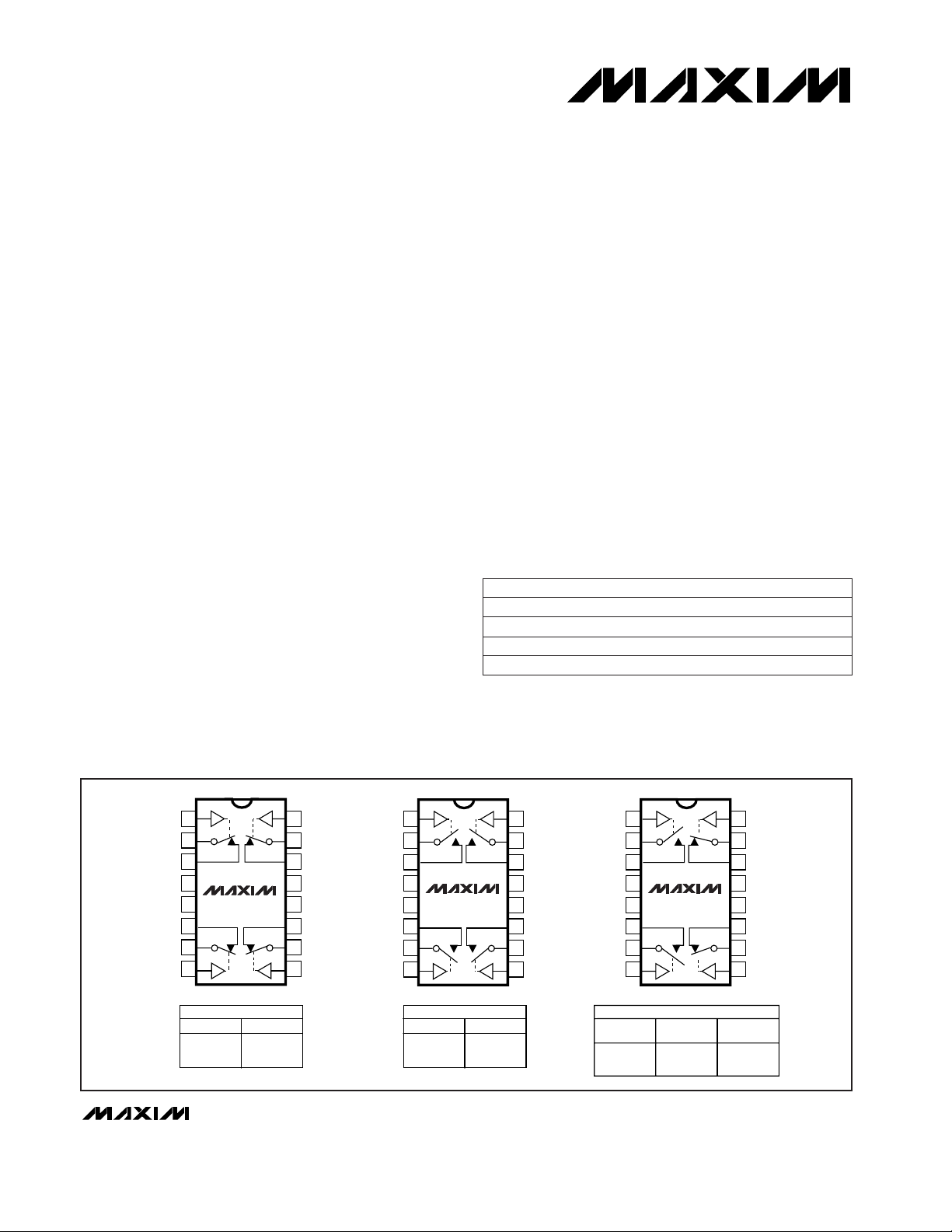
SWITCHES SHOWN FOR LOGIC "0" INPUT
DIP/SO/QSOP
MAX4522
LOGIC SWITCH
0
1
OFF
ON
TOP VIEW
DIP/SO/QSOP
MAX4521
LOGIC SWITCH
0
1
ON
OFF
DIP/SO/QSOP
MAX4523
LOGIC
SWITCHES
1, 4
0
1
OFF
ON
SWITCHES
2, 3
ON
OFF
16
15
14
13
12
11
10
9
1
2
3
4
5
6
7
8
IN2
COM2
NC2
V+
V-
NO1
COM1
IN1
MAX4523
N.C.
NC3
COM3
IN3
IN4
COM4
NO4
GND
16
15
14
13
12
11
10
9
1
2
3
4
5
6
7
8
IN2
COM2
NC2
V+
V-
NC1
COM1
IN1
MAX4521
N.C.
NC3
COM3
IN3
IN4
COM4
NC4
GND
16
15
14
13
12
11
10
9
1
2
3
4
5
6
7
8
IN2
COM2
NO2
V+
V-
NO1
COM1
IN1
MAX4522
N.C.
NO3
COM3
IN3
IN4
COM4
NO4
GND
N.C. = NOT CONNECTED
_____________________Pin Configurations/Functional Diagrams/Truth Tables
19-1136; Rev 1; 1/97
PART
MAX4521CPE
MAX4521CSE
MAX4521CEE 0°C to +70°C
0°C to +70°C
0°C to +70°C
TEMP. RANGE PIN-PACKAGE
16 Plastic DIP
16 Narrow SO
16 QSOP
______________Ordering Information
Ordering Information continued at end of data sheet.
*
Contact factory for dice specifications.
MAX4521C/D 0°C to +70°C Dice*
TOP VIEW
For free samples & the latest literature: http://www.maxim-ic.com, or phone 1-800-998-8800.
For small orders, phone 408-737-7600 ext. 3468.
MAX4521/MAX4522/MAX4523
Quad, Low-Voltage, SPST Analog Switches
2 _______________________________________________________________________________________
ABSOLUTE MAXIMUM RATINGS
ELECTRICAL CHARACTERISTICS—Dual Supplies
(V+ = +4.5V to +5.5V, V- = -4.5V to -5.5V, TA= T
MIN
to T
MAX
, unless otherwise noted. Typical values are at TA= +25°C.)
Note 1: Signals on NC_, NO_, COM_, or IN_ exceeding V+ or V- are clamped by internal diodes. Limit forward-diode current to
maximum current rating.
Note 2: All leads are soldered or welded to PC boards.
Stresses beyond those listed under “Absolute Maximum Ratings” may cause permanent damage to the device. These are stress ratings only, and functional
operation of the device at these or any other conditions beyond those indicated in the operational sections of the specifications is not implied. Exposure to
absolute maximum rating conditions for extended periods may affect device reliability.
Voltages Referenced to GND
V+.....................................................................-0.3V to +13.0V
V-.....................................................................-13.0V to +0.3V
V+ to V-............................................................-0.3V to +13.0V
All Other Pins (Note 1)..........................(V- - 0.3V) to (V+ + 0.3V)
Continuous Current into Any Terminal..............................±10mA
Peak Current into Any Terminal
(pulsed at 1ms,10% duty cycle)...................................±20mA
ESD per Method 3015.7 ..................................................>2000V
Continuous Power Dissipation (T
A
= +70°C) (Note 2)
Plastic DIP (derate 10.53mW/°C above +70°C) ..........842mW
Narrow SO (derate 8.70mW/°C above +70°C) ............696mW
QSOP (derate 9.52mW/°C above +70°C)....................762mW
CERDIP (derate 10.00mW/°C above +70°C)...............800mW
Operating Temperature Ranges
MAX452_C_E......................................................0°C to +70°C
MAX452_E_E ...................................................-40°C to +85°C
MAX452_MJE ................................................-55°C to +125°C
Storage Temperature Range.............................-65°C to +150°C
Lead Temperature (soldering, 10 sec)............................+300°C
(Note 4)
V+ = 5.5V, V- = -5.5V,
V
COM_
= ±4.5V
V+ = 5.5V, V- = -5.5V,
V
COM_
= ±4.5V, VN_= 4.5V
V+ = 5V, V- = -5V,
V
COM_
= ±3V, I
COM_
= 1mA
V+ = 5.5V, V- = -5.5V,
V
COM_
= 4.5V, VN_= ±4.5V
V+ = 5V, V- = -5V,
V
COM_
= ±3V, I
COM_
= 1mA
V+ = 5V, V- = -5V,
V
COM_
= ±3V, I
COM_
= 1mA
CONDITIONS
nA
-200 200
I
COM_(ON)
COM_ On-Leakage Current
(Note 7)
-20 20
-2 0.01 2
nA
-100 100
I
COM_(OFF)
COM_ Off-Leakage Current
(Note 7)
-10 10
-1 0.01 1
nA
-100 100
I
NO_(OFF)
,
I
NC_(OFF)
NO_, NC_ Off-Leakage Current
(Note 7)
-10 10
-1 0.01 1
VV- V+
V
COM_
, V
NO_
,
V
NC_
Analog Signal Range
Ω
15
R
FLAT(ON)
COM_ to NO_, COM_ to NC_
On-Resistance Flatness
(Note 6)
7 12
Ω
6
∆R
ON
COM_ to NO_, COM_ to NC_
On-Resistance Match Between
Channels (Note 5)
65 100
Ω
125
R
ON
COM_ to NO_, COM_ to NC_
On-Resistance
1 4
UNITS
MIN TYP MAX
(Note 3)
SYMBOLPARAMETER
C, E, M
M
C, E
+25°C
M
C, E
C, E, M
+25°C
M
+25°C
C, E, M
+25°C
C, E, M
+25°C
C, E
+25°C
T
A
ANALOG SWITCH
±
±
MAX4521/MAX4522/MAX4523
Quad, Low-Voltage, SPST Analog Switches
_______________________________________________________________________________________ 3
ELECTRICAL CHARACTERISTICS—Dual Supplies (continued)
(V+ = +4.5V to +5.5V, V- = -4.5V to -5.5V, TA= T
MIN
to T
MAX
, unless otherwise noted. Typical values are at TA= +25°C.)
CONDITIONS
C, E, M
C, E, M
V0.8 1.6V
IN_L
IN_ Input Logic Threshold Low
V1.6 2.4V
IN_H
IN_ Input Logic Threshold High
UNITS
MIN TYP MAX
(Note 3)
SYMBOLPARAMETER T
A
C, E, MV
IN_
= 0.8V or 2.4V µA-1 0.03 1I
INH_
, I
INL_
IN_ Input Current Logic High
or Low
+25°C 45 80
Turn-On Time t
ON
V
COM_
= ±3V, V+ = 4.5V,
V- = -4.5V, Figure 1
C, E, M 100
ns
+25°C 15 30
Turn-Off Time t
OFF
V
COM_
= ±3V, V+ = 4.5V,
V- = -4.5V, Figure 1
C, E, M 40
ns
Break-Before-Make Time Delay
(MAX4523 Only)
t
BBM
V
COM_
= ±3V, V+ = 5.5V,
V- = -5.5V, Figure 2
+25°C 5 20 ns
Charge Injection (Note 4) Q
CL= 1nF, V
NO_
= 0V, RS= 0Ω,
Figure 3
+25°C 1 5 pC
NO_, NC_ Off-Capacitance C
N_(OFF)
V
NO_
= GND, f = 1MHz,
Figure 6
+25°C 2 pF
COM_ Off-Capacitance C
COM_(OFF)
V
COM_
= GND, f = 1MHz,
Figure 6
+25°C 2 pF
COM_ On-Capacitance C
COM_(ON)
V
COM_
= V
NO_
= GND,
f = 1MHz, Figure 7
+25°C 5 pF
Off-Isolation (Note 8) V
ISO
RL= 50Ω, CL= 15pF,
VN_= 1V
RMS
, f = 100kHz,
Figure 4
+25°C < -90 dB
Power-Supply Range V+, V- C, E, M -6 6 V
-1 0.05 1
V+ Supply Current I+ V+ = 5.5V, all V
IN_
= 0V or V+
C, E, M -1 1
µA
+25°C -1 0.05 1
V- Supply Current I- V- = -5.5V
C, E, M -1 1
µA
+25°C
Channel-to-Channel Crosstalk
(Note 9)
V
CT
RL= 50, CL= 15pF,
VN_= 1V
RMS
, f = 100kHz,
Figure 5
+25°C < -90 dB
POWER SUPPLY
LOGIC INPUT
SWITCH DYNAMIC CHARACTERISTICS
MAX4521/MAX4522/MAX4523
Quad, Low-Voltage, SPST Analog Switches
4 _______________________________________________________________________________________
ELECTRICAL CHARACTERISTICS—Single +5V Supply
(V+ = +4.5V to +5.5V, V- = 0V, TA= T
MIN
to T
MAX
, unless otherwise noted. Typical values are at TA= +25°C.)
+25°C
(Note 4)
CONDITIONS
C, E, M
125 200
V0 V+
V
COM_
, V
NO_
,
V
NC_
Analog Signal Range
UNITS
MIN TYP MAX
(Note 3)
SYMBOLPARAMETER T
A
COM_ to NO_, COM_ to NC_
On-Resistance
R
ON
V+ = 4.5V, V
COM_
= 3.5V,
I
COM_
= 1mA
C, E, M 250
Ω
+25°C 2 8
COM_ to NO_, COM_ to NC_
On-Resistance Match Between
Channels (Note 5)
∆R
ON
V+ = 5V, V
COM_
= 3.5V,
I
COM_
= 1mA
C, E, M 10
Ω
+25°C -1 0.01 1
C, E -10 10
NO_, NC_ Off-Leakage Current
(Notes 7, 10)
I
NO_(OFF)
,
I
NC_(OFF)
V+ = 5.5V; V
COM_
= 1V, 4.5V;
VN_= 4.5V, 1V
M -100 100
nA
+25°C -1 0.01 1
C, E -10 10
COM_ Off-Leakage Current
(Notes 7, 10)
I
COM_(OFF)
V+ = 5.5V; V
COM_
= 1V, 4.5V;
VN_= 4.5V, 1V
M -100 100
nA
+25°C -2 0.01 2
C, E, -20 20
COM_ On-Leakage Current
(Notes 7, 10)
I
COM_(ON)
V+ = 5.5V; V
COM_
= 4.5V, 1V
M -200 200
nA
IN_ Input Logic Threshold High V
IN_H
C, E 1.6 2.4 V
IN_ Input Logic Threshold Low V
IN_L
C, E 0.8 1.6 V
IN_ Input Current Logic High
or Low
I
INH_
, I
INL_
V
IN_
= 0.8V or 2.4V C, E -1 0.03 1 µA
+25°C 60 100
Turn-On Time t
ON
V
COM_
= 3V, V+ = 4.5V,
Figure 1
C, E, M 150
ns
+25°C 20 50
Turn-Off Time t
OFF
V
COM_
= 3V, V+ = 4.5V,
Figure 1
C, E, M 75
ns
+25°C 10 30
Break-Before-Make Time Delay
(MAX4523 Only)
t
BBM
V
COM_
= 3V, V+ = 5.5V,
Figure 2
ns
+25°C -1 0.05 1
V+ Supply Current I+ V+ = 5.5V, all V
IN_
= 0V or V+
C, E, M -1 1
µA
+25°C -1 0.05 1
V- Supply Current I- V- = 0V
C, E, M -1 1
µA
Charge Injection (Note 4) Q
CL= 1nF, V
NO_
= 0V, RS= 0Ω,
Figure 3
+25°C 1 5 pC
POWER SUPPLY
SWITCH DYNAMIC CHARACTERISTICS
LOGIC INPUT
ANALOG SWITCH

MAX4521/MAX4522/MAX4523
Quad, Low-Voltage, SPST Analog Switches
_______________________________________________________________________________________ 5
Note 3: The algebraic convention is used in this data sheet; the most negative value is shown in the minimum column.
Note 4: Guaranteed by design.
Note 5: ∆R
ON
= ∆R
ON(MAX)
- ∆R
ON(MIN)
.
Note 6: Resistance flatness is defined as the difference between the maximum and minimum on-resistance values, as measured
over the specified analog signal range.
Note 7: Leakage parameters are 100% tested at maximum rated temperature, and guaranteed by correlation at T
A
= +25°C.
Note 8: Off-isolation = 20log10 [ V
COM_
/ (V
NC_
or V
NO_
) ], V
COM_
= output, V
NC_
or V
NO_
= input to off switch.
Note 9: Between any two switches.
Note 10: Leakage testing for single-supply operation is guaranteed by testing with dual supplies.
ELECTRICAL CHARACTERISTICS—Single +3V Supply
(V+ = +2.7V to +3.6V, V- = 0V, TA= T
MIN
to T
MAX
, unless otherwise noted. Typical values are at TA= +25°C.)
+25°C
(Note 4)
COM_ to NO_, COM_ to NC_
On-Resistance
R
ON
V+ = 2.7V, V
COM_
= 1.0V,
I
COM_
= 0.1mA
C, E, M 600
Ω
IN_ Input Logic Threshold High V
IN_H
C, E 1.6 2.4 V
IN_ Input Logic Threshold Low
CONDITIONS
C, E, M
V
IN_L
260 500
V0 V+
V
COM_
, V
NO_
,
V
NC_
Analog Signal Range
C, E 0.8 1.6 V
IN_ Input Current Logic High
or Low
I
INH_
, I
INL_
V
IN_
= 0.8V or 2.4V C, E -1 0.03 1 µA
+25°C 120 250
Turn-On Time t
ON
V
COM_
= 1.5V, V+ = 2.7V,
Figure 1
C, E, M 300
ns
+25°C 40 80
Turn-Off Time t
OFF
V
COM_
= 1.5V, V+ = 2.7V,
Figure 1
C, E, M 100
ns
+25°C 15 50
Break-Before-Make Time Delay
(MAX4523 Only)
t
BBM
V
COM_
= 1.5V, V+ = 3.6V,
Figure 2
ns
+25°C -1 0.05 1
V+ Supply Current
UNITS
MIN TYP MAX
(Note 3)
SYMBOLPARAMETER
I+ V+ = 3.6V, all V
IN_
= 0V or V+
C, E, M -1 1
µA
+25°C -1 0.05 1
V- Supply Current I- V- = 0V
C, E, M -1 1
µA
T
A
Charge Injection Q
CL= 1nF, V
NO_
= 0V, RS= 0Ω,
Figure 3
+25°C 0.5 5 pC
ANALOG SWITCH
LOGIC INPUT
SWITCH DYNAMIC CHARACTERISTICS (Note 4)
POWER SUPPLY

MAX4521/MAX4522/MAX4523
Quad, Low-Voltage, SPST Analog Switches
6 _______________________________________________________________________________________
__________________________________________Typical Operating Characteristics
(V+ = +5V, V- = -5V, GND = 0V, TA = +25°C, unless otherwise noted.)
100
0
-5 -3 1 5
ON-RESISTANCE vs. V
COM
(DUAL SUPPLIES)
20
80
MAX4521/2/3-TOC01
V
COM
(V)
R
ON
(Ω)
-1 3-4 -2 20 4
60
160
180
140
120
40
V+, V- = 2.0V
V+, V- = 3.0V
V+, V- = 4.0V
V+, V- = 5.0V
80
30
-5 -3 1 5
ON-RESISTANCE vs. V
COM
AND
TEMPERATURE (DUAL SUPPLIES)
40
70
MAX4521/2/3-TOC02
V
COM
(V)
R
ON
(Ω)
-1 3-4 -2 20 4
60
110
100
90
50
TA = +125°C
TA = +85°C
TA = +25°C
TA = 0°C
TA = -55°C
250
0
0 1 3 5
ON-RESISTANCE vs. V
COM
(SINGLE SUPPLY)
50
200
MAX4521/2/3-TOC03
V
COM
(V)
R
ON
(Ω)
2 4
150
350
300
100
V+ = 2.7V
V+ = 3.3V
V+ = 5.0V
160
60
0 1 3 5
ON-RESISTANCE vs. V
COM
AND
TEMPERATURE (SINGLE SUPPLY)
80
140
MAX4521/2/3-TOC04
V
COM
(V)
R
ON
(Ω)
2 4
120
200
180
100
TA = +25°C
TA = +125°C
TA = +85°C
TA = 0°C
TA = -55°C
200
0
2 4 8 12
TURN-ON/OFF TIME vs.
SUPPLY VOLTAGE
40
160
t
ON
t
OFF
MAX4521/2/3-TOC07
t
ON
, t
OFF
(ns)
V+ (V)
6 103 7 115 9
120
80
180
20
140
100
60
10n
0.1p
-55 -25 0 25 75
ON- AND OFF-LEAKAGE CURRENT
vs. TEMPERATURE
1p
1n
MAX4521/2/3-TOC05
TEMPERATURE (°C)
LEAKAGE (A)
50 100 125
100p
10p
ON LEAKAGE
OFF LEAKAGE
2
-2
-5 -3 1 5
CHARGE INJECTION
vs.V
COM
1
MAX4521/2/3-TOC06
V
COM
(V)
Q (pC)
-1 3-4 -2 20 4
0
-1
V+ = +5V
V- = 0V
V+ = +5V
V- = -5V
100
0
-55 -25 75
TURN-ON/OFF TIME
vs. TEMPERATURE
20
80
t
ON
t
OFF
MAX4521/2/3-TOC08
TEMPERATURE (°C)
t
ON
, t
OFF
(ns)
25 500 125100
60
40
90
10
70
50
30
1
0.00001
-55 -25 75
POWER-SUPPLY CURRENT
vs. TEMPERATURE
0.0001
0.1
I+
I-
MAX4521/2/3-TOC09
TEMPERATURE (°C)
I+, I- (µA)
25 500 125100
0.01
0.001

MAX4521/MAX4522/MAX4523
Quad, Low-Voltage, SPST Analog Switches
_______________________________________________________________________________________ 7
100
0.001
10 1k100 100k10k
TOTAL HARMONIC DISTORTION
vs. FREQUENCY
0.01
MAX4521/2/3-TOC10
FREQUENCY (Hz)
THD (%)
0.1
1
10
V+ = +5V
V- = -5V
600Ω IN AND OUT
0
-10
-90
0.01 0.1 1 10 100 300
FREQUENCY RESPONSE
-80
-70
MAX4521/2/3-TOC11
FREQUENCY (MHz)
LOSS (dB)
PHASE (DEGREES)
-50
-60
-40
-20
-30
5
0
-40
-35
-30
-20
-25
-15
-5
-10
INSERTION LOSS
50Ω IN/OUT
OFF-ISOLATION
ON-PHASE
_____________________________Typical Operating Characteristics (continued)
(V+ = +5V, V- = -5V, GND = 0V, TA= +25°C, unless otherwise noted.)
______________________________________________________________Pin Description
NAME FUNCTION
1, 16, 9, 8 IN1–IN4 Logic-Control Digital Inputs
2, 15, 10, 7 COM1–COM4 Analog Switch Common* Terminals
PIN
3, 14, 11, 6 NC1–NC4 Analog Switch Normally Closed Terminals
4 V-
Negative Analog Supply-Voltage Input. Connect to GND for singlesupply operation.
13 V+
Positive Analog and Digital Supply Voltage Input. Internally connected to substrate.
12 N.C. No Connect. Not internally connected.
5 GND
Ground. Connect to digital ground. (Analog signals have no ground
reference; they are limited to V+ and V-.)
*NO_ (or NC_) and COM_ pins are identical and interchangeable. Either may be considered as an input or output; signals pass
equally well in either direction.
1, 16, 9, 8
2, 15, 10, 7
—
4
13
12
5
1, 16, 9, 8
2, 15, 10, 7
—
4
13
12
5
MAX4521 MAX4522 MAX4523
— NO1–NO4 Analog Switch Normally Open Terminals3, 14, 11, 6 —
— NO1, NO4 Analog Switch Normally Open Terminals— 3, 6
— NC2, NC3 Analog Switch Normally Closed Terminals— 14, 11

MAX4521/MAX4522/MAX4523
__________Applications Information
Power-Supply Considerations
Overview
The MAX4521/MAX4522/MAX4523 construction is typical of most CMOS analog switches. They have three
supply pins: V+, V-, and GND. V+ and V- are used to
drive the internal CMOS switches, and they set the limits of the analog voltage on any switch. Reverse ESDprotection diodes are internally connected between
each analog-signal pin and both V+ and V-. If any analog signal exceeds V+ or V-, one of these diodes conducts. During normal operation these reverse-biased
ESD diodes leak, forming the only current drawn from
V+ or V-.
Virtually all the analog leakage current is through the
ESD diodes. Although the ESD diodes on a given signal pin are identical and therefore fairly well balanced,
they are reverse biased differently. Each is biased by
either V+ or V- and the analog signal. This means their
leakages vary as the signal varies. The
difference
in the
two diode leakages from the signal path to the V+ and
V- pins constitutes the analog-signal-path leakage current. All analog leakage current flows to the supply terminals, not to the other switch terminal. This explains
how both sides of a given switch can show leakage
currents of the same or opposite polarity.
There is no connection between the analog-signal
paths and GND. The analog-signal paths consist of an
N-channel and P-channel MOSFET with their sources
and drains paralleled, and their gates driven out of
phase to V+ and V- by the logic-level translators.
V+ and GND power the internal logic and logic-level
translators, and set the input logic thresholds. The
logic-level translators convert the logic levels to
switched V+ and V- signals, to drive the gates of the
analog switches. This drive signal is the only connection between the logic supplies and the analog supplies. V+ and V- have ESD-protection diodes to GND.
The logic-level inputs and output have ESD protection
to V+ and to GND.
Increasing V- has no effect on the logic-level thresholds, but it does increase the drive to the P-channel
switches, reducing their on-resistance. V- also sets the
negative limit of the analog-signal voltage.
The logic-level thresholds are CMOS/TTL compatible
when V+ = +5V. The threshold increases slightly as V+
is raised, and when V+ reaches +12V, the level threshold is about 3.1V. This is above the TTL output highlevel minimum of 2.8V, but still compatible with CMOS
outputs.
Bipolar Supplies
The MAX4521/MAX4522/MAX4523 operate with bipolar
supplies between ±2V and ±6V. The V+ and V- supplies need not be symmetrical, but their sum cannot
exceed the absolute maximum rating of 13.0V. Do not
connect the MAX4521/MAX4522/MAX4523 V+ to +3V,
and then connect the logic-level-input pins to TTL
logic-level signals. TTL logic-level outputs in excess
of the absolute maximum ratings can damage the
part and/or external circuits.
Caution: The absolute maximum V+ to V- differential
voltage is 13.0V. Typical ±6V or 12V supplies with
±10% tolerances can be as high as 13.2V. This voltage
can damage the MAX4521/MAX4522/MAX4523. Even
±5% tolerance supplies may have overshoot or noise
spikes that exceed 13.0V.
Single Supply
The MAX4521/MAX4522/MAX4523 operate from a
single supply between +2V and +12V when V- is connected to GND. All of the bipolar precautions must be
observed.
High-Frequency Performance
In 50Ω systems, signal response is reasonably flat up
to 50MHz (see
Typical Operating Characteristics
).
Above 20MHz, the on-response has several minor
peaks that are highly layout dependent. The problem
with high-frequency operation is not turning the switch
on, but turning it off. The off-state switch acts like a
capacitor and passes higher frequencies with less
attenuation. At 10MHz, off-isolation is about -52dB in
50Ω systems, becoming worse (approximately 20dB
per decade) as frequency increases. Higher circuit
impedances also make off-isolation worse. Adjacent
channel attenuation is about 3dB above that of a bare
IC socket, and is due entirely to capacitive coupling.
Quad, Low-Voltage, SPST Analog Switches
8 _______________________________________________________________________________________

MAX4521/MAX4522/MAX4523
Quad, Low-Voltage, SPST Analog Switches
_______________________________________________________________________________________ 9
V
GEN
GND
NC or
NO
C
L
V
OUT
V-
V-
V+
V
OUT
IN
OFF
ON
OFF
∆V
OUT
Q = (∆V
OUT
)(CL)
COM
IN DEPENDS ON SWITCH CONFIGURATION;
INPUT POLARITY DETERMINED BY SENSE OF SWITCH.
OFF
ON
OFF
IN
V
IN
= +3V
V+
R
GEN
IN
MAX4521
MAX4522
MAX4523
Figure 3. Charge Injection
tr < 20ns
tf < 20ns
50%
0V
LOGIC
INPUT
V-
V-
R
L
300Ω
NO
or NC
GND
C
L
INCLUDES FIXTURE AND STRAY CAPACITANCE.
V
OUT
= V
COM (
R
L
)
RL + R
ON
SWITCH
INPUT
IN
+3V
t
OFF
0V
COM
SWITCH
OUTPUT
0.9 x V
0UT
0.9 x V
OUT
t
ON
V
OUT
SWITCH
OUTPUT
LOGIC
INPUT
LOGIC INPUT WAVEFORMS INVERTED FOR SWITCHES
THAT HAVE THE OPPOSITE LOGIC SENSE.
V+
C
L
35pF
V+
V
OUT
V
COM
0V
MAX4521
MAX4522
MAX4523
Figure 1. Switching Time
Figure 2. Break-Before-Make Interval (MAX4523 only)
______________________________________________Test Circuits/Timing Diagrams
MAX4523
LOGIC
INPUT
V
V
COM1
COM1
COM2
COM2
IN1, 2
GND
C
INCLUDES FIXTURE AND STRAY CAPACITANCE.
L
V+
V+
NO
NC
V-
V-
V
OUT2
R
C
L2
L2
RL = 300Ω
= 35pF
C
L
V
OUT1
R
C
L1
L1
LOGIC
INPUT
SWITCH
OUTPUT 1
(V
SWITCH
OUTPUT 2
(V
OUT1
OUT2
+3V
50%
0V
0.9 x V
0UT1
0V
)
)
0V
t
D
0.9 x V
t
D
OUT2

MAX4521/MAX4522/MAX4523
Quad, Low-Voltage, SPST Analog Switches
10 ______________________________________________________________________________________
Figure 5. Crosstalk
IN
0V or
2.4V
SIGNAL
GENERATOR 0dBm
V+
10nF
ANALYZER
NC
or NO
R
L
GND
COM
10nF
V-
V-
V+
MAX4521
MAX4522
MAX4523
Figure 4. Off Isolation
_________________________________Test Circuits/Timing Diagrams (continued)
CAPACITANCE
METER
NC
or NO
COM
GND
10nF
V-
V-
IN
0V or
2.4V
10nF
V+
f = 1MHz
V+
MAX4521
MAX4522
MAX4523
Figure 7. Channel-On Capacitance
CAPACITANCE
METER
NC
or NO
COM
GND
10nF
V-
V-
IN
0V or
2.4V
10nF
V+
f = 1MHz
V+
MAX4521
MAX4522
MAX4523
Figure 6. Channel-Off Capacitance
MAX4521
SIGNAL
GENERATOR 0dBm
10nF
V+
V+
COM1
N01
MAX4522
MAX4523
50Ω
ANALYZER
0V or 2.4V
R
V-
V-
IN2
COM2
0V or 2.4V
NC
10nF
IN1
N02
GND
L

MAX4521/MAX4522/MAX4523
Quad, Low-Voltage, SPST Analog Switches
______________________________________________________________________________________ 11
PART
MAX4521EPE
MAX4521ESE
MAX4522CPE
0°C to +70°C
-40°C to +85°C
-40°C to +85°C
TEMP. RANGE PIN-PACKAGE
16 Plastic DIP
16 Narrow SO
16 Plastic DIP
MAX4522CSE 0°C to +70°C 16 Narrow SO
MAX4522CEE 0°C to +70°C 16 QSOP
MAX4522C/D 0°C to +70°C Dice*
MAX4522EPE -40°C to +85°C 16 Plastic DIP
MAX4522ESE -40°C to +85°C 16 Narrow SO
MAX4522EEE -40°C to +85°C 16 QSOP
MAX4522MJE -55°C to +125°C 16 CERDIP**
MAX4523CPE
0°C to +70°C 16 Plastic DIP
MAX4523CSE 0°C to +70°C 16 Narrow SO
MAX4523CEE 0°C to +70°C 16 QSOP
MAX4523C/D 0°C to +70°C Dice*
MAX4523EPE -40°C to +85°C 16 Plastic DIP
MAX4523ESE -40°C to +85°C 16 Narrow SO
MAX4523EEE -40°C to +85°C 16 QSOP
MAX4523MJE -55°C to +125°C 16 CERDIP**
_Ordering Information (continued)
*
Contact factory for dice specifications.
**
Contact factory for availability.
___________________Chip Topography
0.057"
(1.45mm)
0.046"
(1.19mm)
COM4
"D"
COM1
IN3
IN2
COM3
COM2
IN1
"B" GND
V-
"A"
"C"
IN4
V+
TRANSISTOR COUNT: 97
SUBSTRATE CONNECTED TO V+
A
B
C
D
A
B
C
D
A
B
C
D
MAX4521 MAX4522 MAX4523
PIN NAME
NAME NAMEPIN PIN
NC1
NC4
NC3
NC2
NO1
NO4
NO3
NO2
NO1
NO4
NC3
NC2
MAX4521EEE
MAX4521MJE -55°C to +125°C
-40°C to +85°C 16 QSOP
16 CERDIP**

MAX4521/MAX4522/MAX4523
Quad, Low-Voltage, SPST Analog Switches
________________________________________________________Package Information
DIM
A
A1
A2
B
C
D
E
e
H
h
L
N
S
α
MIN
0.061
0.004
0.055
0.008
0.0075
0.150
0.230
0.010
0.016
0°
MAX
0.068
0.0098
0.061
0.012
0.0098
0.157
0.244
0.016
0.035
8°
MIN
1.55
0.127
1.40
0.20
0.19
3.81
5.84
0.25
0.41
0°
MAX
1.73
0.25
1.55
0.31
0.25
3.99
6.20
0.41
0.89
8°
INCHES MILLIMETERS
21-0055A
QSOP
QUARTER
SMALL-OUTLINE
PACKAGE
DIM
D
S
D
S
D
S
D
S
MIN
0.189
0.0020
0.337
0.0500
0.337
0.0250
0.386
0.0250
MAX
0.196
0.0070
0.344
0.0550
0.344
0.0300
0.393
0.0300
MIN
4.80
0.05
8.56
1.27
8.56
0.64
9.80
0.64
MAX
4.98
0.18
8.74
1.40
8.74
0.76
9.98
0.76
INCHES MILLIMETERS
PINS
16
16
20
20
24
24
28
28
L
α
H
A2
E
E
D
e
A
A1
C
B
S
N
h x 45°
SEE VARIATIONS
SEE VARIATIONS
SEE VARIATIONS
0.635 BSC0.25 BSC
DIM
A
A1
B
C
E
e
H
L
MIN
0.053
0.004
0.014
0.007
0.150
0.228
0.016
MAX
0.069
0.010
0.019
0.010
0.157
0.244
0.050
MIN
1.35
0.10
0.35
0.19
3.80
5.80
0.40
MAX
1.75
0.25
0.49
0.25
4.00
6.20
1.27
INCHES MILLIMETERS
21-0041A
Narrow SO
SMALL-OUTLINE
PACKAGE
(0.150 in.)
DIM
D
D
D
MIN
0.189
0.337
0.386
MAX
0.197
0.344
0.394
MIN
4.80
8.55
9.80
MAX
5.00
8.75
10.00
INCHES MILLIMETERS
PINS
8
14
16
1.270.050
L
0°-8°
HE
D
e
A
A1
C
0.101mm
0.004in.
B
Maxim cannot assume responsibility for use of any circuitry other than circuitry entirely embodied in a Maxim product. No circuit patent licenses are
implied. Maxim reserves the right to change the circuitry and specifications without notice at any time.
12
____________________Maxim Integrated Products, 120 San Gabriel Drive, Sunnyvale, CA 94086 408-737-7600
© 1997 Maxim Integrated Products Printed USA is a registered trademark of Maxim Integrated Products.
 Loading...