Maxim MAX4502C-D, MAX4501MJA, MAX4501EXK-T, MAX4501EUK-T, MAX4501ESA Datasheet
...
_________________General Description
The MAX4501/MAX4502 are single-pole/single-throw
(SPST), low-voltage, single-supply, CMOS analog
switches. The MAX4501 is normally open (NO). The
MAX4502 is normally closed (NC).
These CMOS switches can operate continuously with a
single supply between +2V and +12V. Each switch can
handle Rail-to-Rail®analog signals. The off-leakage
current is only 1nA at +25°C or 10nA at +85°C.
The digital input has 0.8V and 2.4V logic thresholds,
ensuring TTL/CMOS-logic compatibility when using a
single +5V supply.
_________________________Applications
Battery-Operated Equipment
Audio and Video Signal Routing
Low-Voltage Data-Acquisition Systems
Communications Circuits
PCMCIA Cards
Cellular Phones
Modems
_____________________________Features
♦ Available in SOT23-5 and SC70-5 Packages
♦ +2V to +12V Single-Supply Operation
♦ Guaranteed On-Resistance: 250Ω at +5V
♦ Guaranteed Low Off-Leakage Current
1nA at +25°C
10nA at +85°C
♦ Guaranteed Low On-Leakage Current
2nA at +25°C
20nA at +85°C
♦ Low Charge Injection: 10pC
♦ Fast Switching Speed: tON= 75ns, t
OF
F
= 50ns
♦ TTL/CMOS-Logic Compatible with +5V Supply
MAX4501/MAX4502
Low-Voltage, SPST, CMOS Analog Switches
________________________________________________________________ Maxim Integrated Products 1
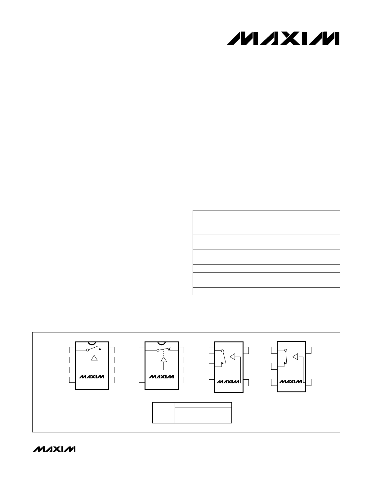
_______________________Pin Configurations/Functional Diagrams/Truth Table
19-1062; Rev 1; 11/99
PART
MAX4501CUK-T
MAX4501CSA
MAX4501CPA 0°C to +70°C
0°C to +70°C
0°C to +70°C
TEMP. RANGE
PIN-
PACKAGE
5 SOT23-5
8 SO
8 Plastic DIP
________________Ordering Information
Ordering Information continued at end of data sheet.
*Contact factory for dice specifications.
**Contact factory for availability.
For free samples & the latest literature: http://www.maxim-ic.com, or phone 1-800-998-8800.
For small orders, phone 1-800-835-8769.
MAX4501C/D 0°C to +70°C Dice*
MAX4501EUK-T -40°C to +85°C 5 SOT23-5
MAX4501ESA -40°C to +85°C 8 SO
MAX4501EPA -40°C to +85°C 8 Plastic DIP
MAX4501MJA -55°C to +125°C 8 CERDIP**
Rail-to-Rail is a registered trademark of Nippon Motorola, Ltd.
MAX4501EXK-T -40°C to +85°C 5 SC70-5
TOP
MARK
AAAA
—
—
—
AAAA
—
—
—
AAE
TOP VIEW
1
1
COM
2
N.C.
3
N.C.
4
V+
N.C. = NOT INTERNALLY CONNECTED
MAX4501
SO/DIP
8
NO
GND
7
IN
6
N.C.
5
COM
N.C.
N.C.
1
2
3
4
V+
MAX4502
SO/DIP
INPUT
LOW
HIGH
8
NC
GND
7
IN
6
N.C.
5
MAX4501
OFF
ON
SWITCH STATE
1
COM
2
NO
3
GND
SC70-5/SOT23-5
MAX4502
ON
OFF
MAX4501
COM
5
V+
2
NC
3
GND
IN
4
MAX4502
SC70-5/SOT23-5
5
V+
IN
4

MAX4501/MAX4502
Low-Voltage, SPST, CMOS Analog Switches
2 _______________________________________________________________________________________
ABSOLUTE MAXIMUM RATINGS
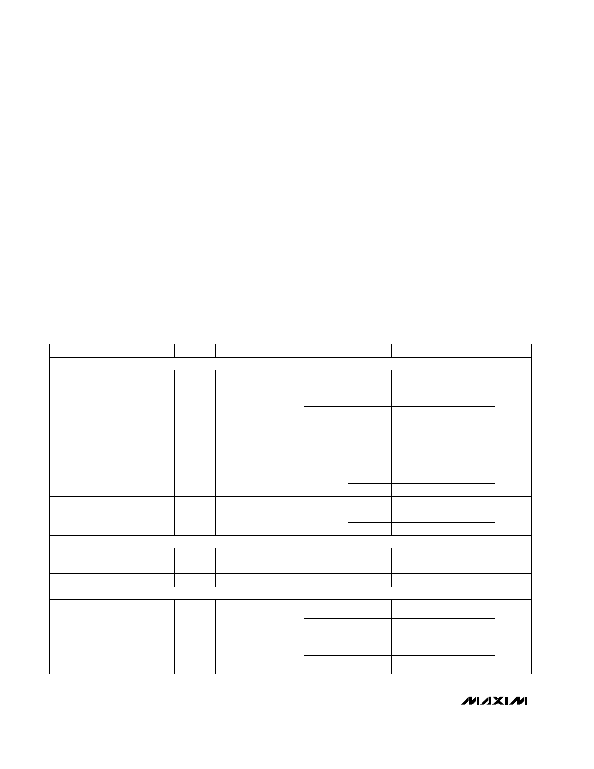
ELECTRICAL CHARACTERISTICS—+5V Supply
(V+ = +4.5V to +5.5V, V
INH
= 2.4V, V
INL
= 0.8V, TA= T
MIN
to T
MAX
, unless otherwise noted. Typical values are at TA= +25°C.) (Note 2)
Stresses beyond those listed under “Absolute Maximum Ratings” may cause permanent damage to the device. These are stress ratings only, and functional
operation of the device at these or any other conditions beyond those indicated in the operational sections of the specifications is not implied. Exposure to
absolute maximum rating conditions for extended periods may affect device reliability.
(Voltages Referenced to GND)
V+ ...........................................................................-0.3V to +13V
Voltage into Any Terminal (Note 1) ..........-0.3V to (V+ + 0.3V) or
±10mA (whichever occurs first)
Continuous Current into Any Terminal..............................±10mA
Peak Current, NO or COM
(pulsed at 1ms, 10% duty cycle)..................................±20mA
ESD per Method 3015.7 ..................................................>2000V
Continuous Power Dissipation (T
A
= +70°C)
5-Pin SC70-5 (derate 2.5mW/°C above +70°C)...........200mW
5-Pin SOT23-5 (derate 7.1mW/°C above +70°C) ........571mW
8-Pin SO (derate 5.88mW/°C above +70°C)................471mW
8-Pin Plastic DIP (derate 9.09mW/°C above +70°C) ...727mW
8-Pin CERDIP (derate 8.00mW/°C above +70°C)........640mW
Operating Temperature Ranges
MAX4501C_ _/MAX4502C_ _ .............................0°C to +70°C
MAX4501E_ _/MAX4502E_ _ ...........................-40°C to +85°C
MAX4501MJA/MAX4502MJA ........................-55°C to +125°C
Storage Temperature Range .............................-65°C to +150°C
Lead Temperature (soldering, 10s) .................................+300°C
VIN= V+, 0
V+ = 5.5V,
V
COM
= 1V,
V
NO
or VNC= 4.5V
CONDITIONS
-1 0.01 1
90 250
V0V+
V
COM
,
VNO, V
NC
Analog Signal Range
16 75
µA-1 0.03 1I
INH
, I
INL
Input Current Logic High or Low
V0 0.8V
INL
Input Logic Low
-10 10
nA
-100 100
I
NO(OFF),
I
NC(OFF)
NO or NC Off-Leakage Current
(Notes 3, 4)
V2.4 V+V
INH
Input Logic High
UNITSMIN TYP MAXSYMBOLPARAMETER
Note 1: Voltages exceeding V+ or GND on any signal terminal are clamped by internal diodes. Limit forward-diode current to
maximum current rating.
V
COM
= 3.5V,
I
COM
= 1mA
Ω
350
R
ON
COM to NO or NC
On-Resistance
TA= +25°C
TA= T
MIN
to T
MAX
TA= +25°C
TA= T
MIN
to T
MAX
C, E
M
C, E
TA= +25°C
M
V+ = 5.5V,
V
COM
= 1V,
VNOor VNC= 4.5V
TA= T
MIN
to T
MAX
-1 0.01 1
-10 10
nA
-100 100
I
COM(OFF)
COM Off-Leakage Current
(Notes 3, 4)
C, E
TA= +25°C
M
V+ = 5.5V,
V
COM
= 1V, 4.5V
TA= T
MIN
to T
MAX
-2 0.01 2
-20 20
nA
-200 200
I
COM(ON)
COM On-Leakage Current
(Notes 3, 4)
VNO= VNC= 1.5V,
VIN= 3V, RL= 1kΩ,
C
L
= 35pF, Figure 1
ns
150
t
ON
Turn-On Time
TA= +25°C
TA= T
MIN
to T
MAX
VNO= VNC= 1.5V,
VIN= 3V, RL= 1kΩ,
C
L
= 35pF, Figure 1
TA= +25°C
TA= T
MIN
to T
MAX
ns
150
t
OFF
Turn-Off Time
10 50
ANALOG SWITCH
DIGITAL I/O
SWITCH DYNAMIC CHARACTERISTICS

MAX4501/MAX4502
Low-Voltage, SPST, CMOS Analog Switches
_______________________________________________________________________________________ 3
CL= 1nF, VNO= 0, RS= 0Ω, TA= +25°C,
Figure 2
VIN= 0 or V+
f = 1MHz, Figure 4
RL= 50Ω, CL= 15pF, VNO= 1V
RMS
,
f = 100kHz, TA= +25°C, Figure 3
f = 1MHz, Figure 4
f = 1MHz, Figure 4
CONDITIONS
pC110QCharge Injection (Note 5)
µA
-10 10
I+V+ Supply Current
-1 1
pF8C
COM(ON)
COM On-Capacitance
dB< -100V
ISO
Off-Isolation
pF3
C
NO(OFF)
,
C
NC(OFF)
NO or NC Off-Capacitance
pF3C
COM(OFF)
COM Off-Capacitance
UNITSMIN TYP MAXSYMBOLPARAMETER
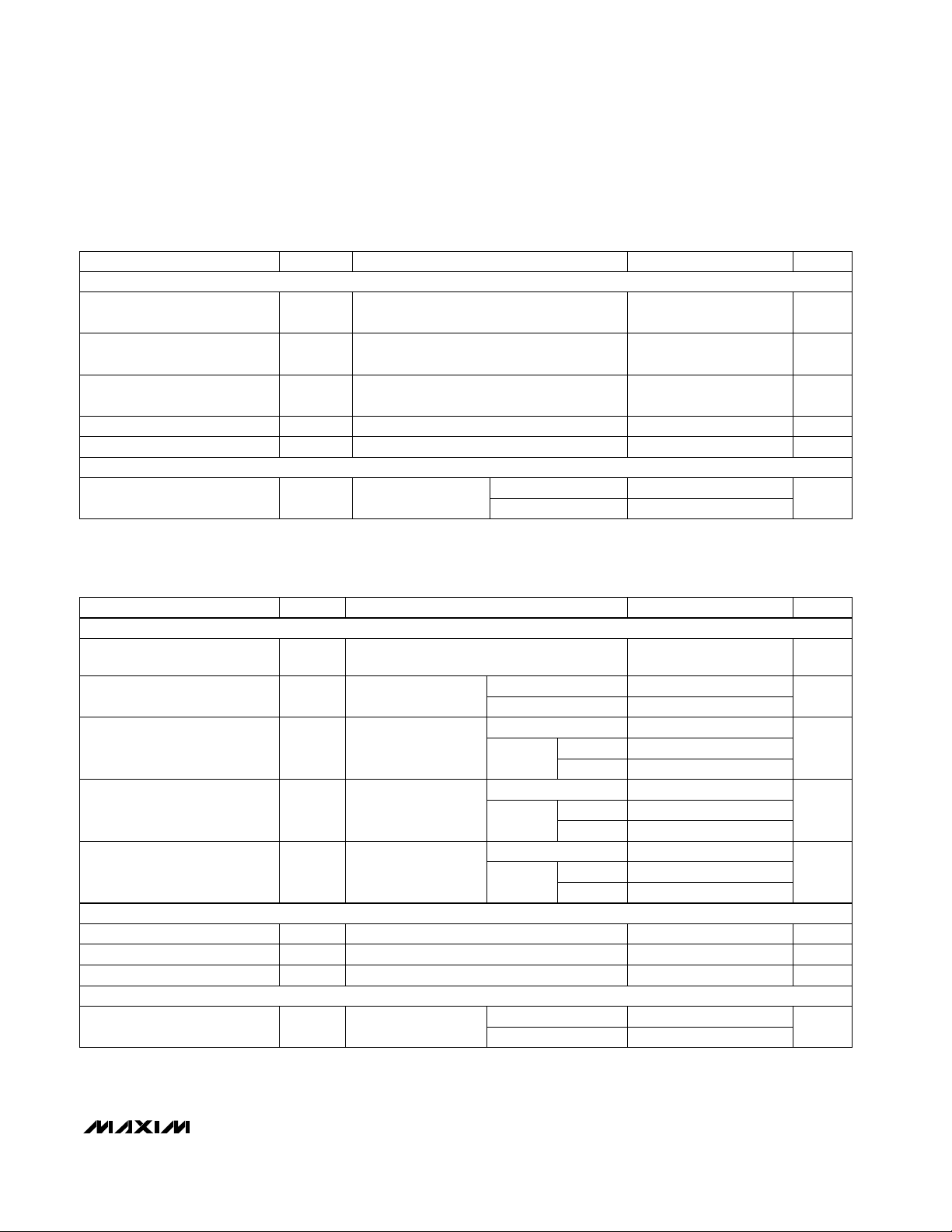
ELECTRICAL CHARACTERISTICS—+5V Supply (continued)
(V+ = +4.5V to +5.5V, V
INH
= 2.4V, V
INL
= 0.8V, TA= T
MIN
to T
MAX
, unless otherwise noted. Typical values are at TA= +25°C.) (Note 2)
ELECTRICAL CHARACTERISTICS—+12V Supply
(V+ = +11.4V to +12.6V, V
INH
= 5.0V, V
INL
= 0.8V, TA= T
MIN
to T
MAX
, unless otherwise noted. Typical values are at TA= +25°C.) (Note 2)
SWITCH DYNAMIC CHARACTERISTICS (continued)
POWER SUPPLY
C, E
TA= +25°C
V
COM
= 10V,
I
COM
= 1mA
µA
-10 10
IN = 0 or V+ I+
VIN= 0 or V+
M
V
COM
= 10V,
V
NO
or VNC= 1V,
V+ = +12.6V
CONDITIONS
Ω
200
R
ON
COM to NO or NC
On-Resistance
TA= +25°C
TA= T
MIN
to T
MAX
C, E
TA= T
MIN
to T
MAX
TA= +25°C
M
V
COM
= 10V,
VNOor VNC= 1V,
V+ = +12.6V
TA= T
MIN
to T
MAX
-5 5
-50 50
nA
-500 500
I
COM(OFF)
COM Off-Leakage Current
(Notes 3, 4)
C, E
TA= +25°C
M
V
COM
= 10V,
V+ = +12.6V
TA= T
MIN
to T
MAX
-10 10
V+ Supply Current
-100 100
-5 5
nA
-1000 1000
40 160
I
COM(ON)
V0V+
V
COM
,
V
NO
, V
NC
Analog Signal Range
COM On-Leakage Current
(Notes 3, 4)
-1 1
µA-1 0.03 1I
INH
, I
INL
Input Current Logic High or Low
V
0 0.8V
INL
Input Logic Low
-50 50
nA
-500 500
I
NO(OFF)
,
I
NC(OFF)
NO or NC Off-Leakage Current
(Notes 3, 4)
5.0 V+V
INH
Input Logic High
UNITSMIN TYP MAXSYMBOLPARAMETER
ANALOG SWITCH
DIGITAL I/O
POWER SUPPLY
V
TA= +25°C
TA= T
MIN
to T
MAX
TA= +25°C
TA= T
MIN
to T
MAX
 Loading...