

_________________General Description
The MAX4501/MAX4502 are single-pole/single-throw
(SPST), low-voltage, single-supply, CMOS analog
switches. The MAX4501 is normally open (NO). The
MAX4502 is normally closed (NC).
These CMOS switches can operate continuously with a
single supply between +2V and +12V. Each switch can
handle Rail-to-Rail®analog signals. The off-leakage
current is only 1nA at +25°C or 10nA at +85°C.
The digital input has 0.8V and 2.4V logic thresholds,
ensuring TTL/CMOS-logic compatibility when using a
single +5V supply.
_________________________Applications
Battery-Operated Equipment
Audio and Video Signal Routing
Low-Voltage Data-Acquisition Systems
Communications Circuits
PCMCIA Cards
Cellular Phones
Modems
_____________________________Features
♦ Available in SOT23-5 and SC70-5 Packages
♦ +2V to +12V Single-Supply Operation
♦ Guaranteed On-Resistance: 250Ω at +5V
♦ Guaranteed Low Off-Leakage Current
1nA at +25°C
10nA at +85°C
♦ Guaranteed Low On-Leakage Current
2nA at +25°C
20nA at +85°C
♦ Low Charge Injection: 10pC
♦ Fast Switching Speed: tON= 75ns, t
OF
F
= 50ns
♦ TTL/CMOS-Logic Compatible with +5V Supply
MAX4501/MAX4502
Low-Voltage, SPST, CMOS Analog Switches
________________________________________________________________ Maxim Integrated Products 1
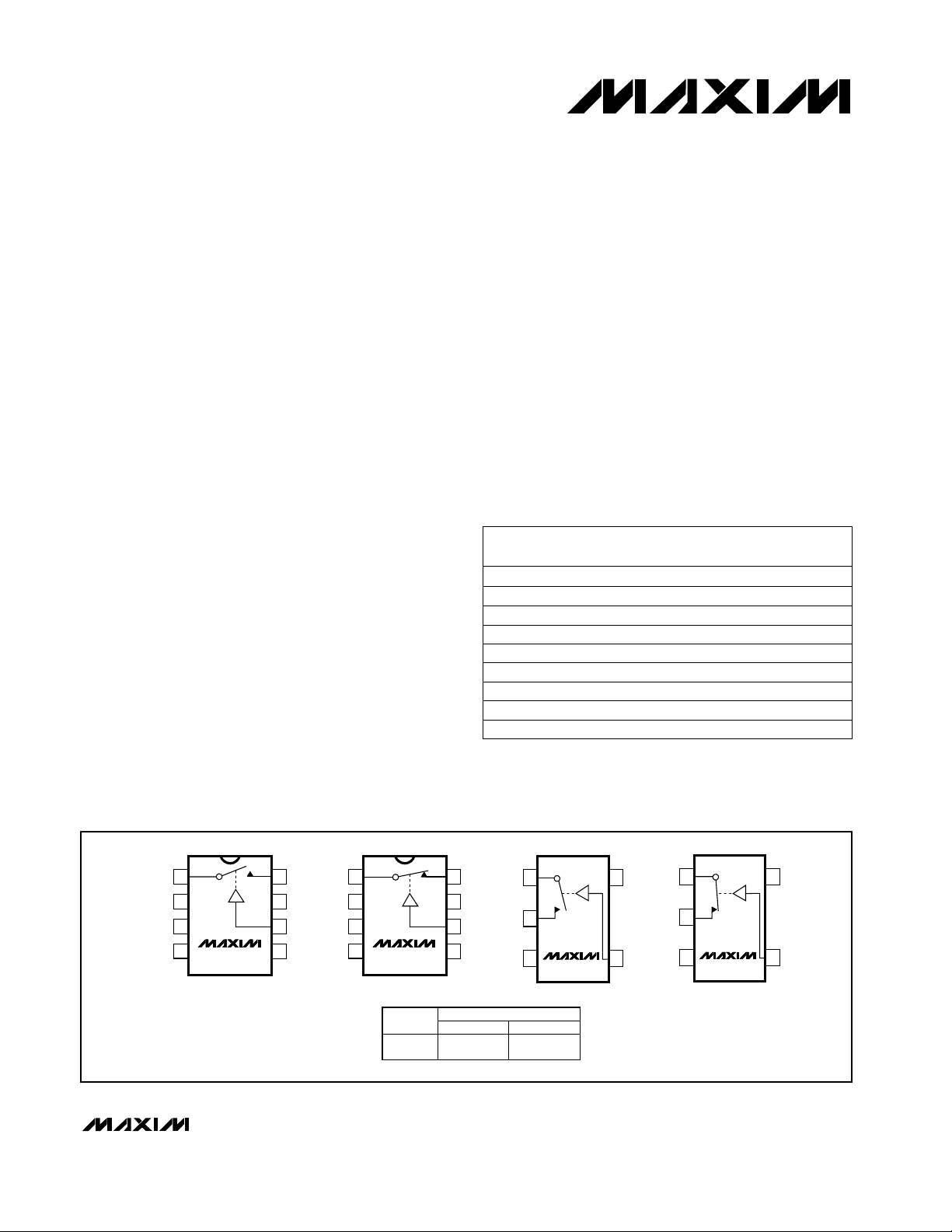
_______________________Pin Configurations/Functional Diagrams/Truth Table
19-1062; Rev 1; 11/99
PART
MAX4501CUK-T
MAX4501CSA
MAX4501CPA 0°C to +70°C
0°C to +70°C
0°C to +70°C
TEMP. RANGE
PIN-
PACKAGE
5 SOT23-5
8 SO
8 Plastic DIP
________________Ordering Information
Ordering Information continued at end of data sheet.
*Contact factory for dice specifications.
**Contact factory for availability.
For free samples & the latest literature: http://www.maxim-ic.com, or phone 1-800-998-8800.
For small orders, phone 1-800-835-8769.
MAX4501C/D 0°C to +70°C Dice*
MAX4501EUK-T -40°C to +85°C 5 SOT23-5
MAX4501ESA -40°C to +85°C 8 SO
MAX4501EPA -40°C to +85°C 8 Plastic DIP
MAX4501MJA -55°C to +125°C 8 CERDIP**
Rail-to-Rail is a registered trademark of Nippon Motorola, Ltd.
MAX4501EXK-T -40°C to +85°C 5 SC70-5
TOP
MARK
AAAA
—
—
—
AAAA
—
—
—
AAE
TOP VIEW
1
1
COM
2
N.C.
3
N.C.
4
V+
N.C. = NOT INTERNALLY CONNECTED
MAX4501
SO/DIP
8
NO
GND
7
IN
6
N.C.
5
COM
N.C.
N.C.
1
2
3
4
V+
MAX4502
SO/DIP
INPUT
LOW
HIGH
8
NC
GND
7
IN
6
N.C.
5
MAX4501
OFF
ON
SWITCH STATE
1
COM
2
NO
3
GND
SC70-5/SOT23-5
MAX4502
ON
OFF
MAX4501
COM
5
V+
2
NC
3
GND
IN
4
MAX4502
SC70-5/SOT23-5
5
V+
IN
4
MAX4501/MAX4502
Low-Voltage, SPST, CMOS Analog Switches
2 _______________________________________________________________________________________
ABSOLUTE MAXIMUM RATINGS
ELECTRICAL CHARACTERISTICS—+5V Supply
(V+ = +4.5V to +5.5V, V
INH
= 2.4V, V
INL
= 0.8V, TA= T
MIN
to T
MAX
, unless otherwise noted. Typical values are at TA= +25°C.) (Note 2)
Stresses beyond those listed under “Absolute Maximum Ratings” may cause permanent damage to the device. These are stress ratings only, and functional
operation of the device at these or any other conditions beyond those indicated in the operational sections of the specifications is not implied. Exposure to
absolute maximum rating conditions for extended periods may affect device reliability.
(Voltages Referenced to GND)
V+ ...........................................................................-0.3V to +13V
Voltage into Any Terminal (Note 1) ..........-0.3V to (V+ + 0.3V) or
±10mA (whichever occurs first)
Continuous Current into Any Terminal..............................±10mA
Peak Current, NO or COM
(pulsed at 1ms, 10% duty cycle)..................................±20mA
ESD per Method 3015.7 ..................................................>2000V
Continuous Power Dissipation (T
A
= +70°C)
5-Pin SC70-5 (derate 2.5mW/°C above +70°C)...........200mW
5-Pin SOT23-5 (derate 7.1mW/°C above +70°C) ........571mW
8-Pin SO (derate 5.88mW/°C above +70°C)................471mW
8-Pin Plastic DIP (derate 9.09mW/°C above +70°C) ...727mW
8-Pin CERDIP (derate 8.00mW/°C above +70°C)........640mW
Operating Temperature Ranges
MAX4501C_ _/MAX4502C_ _ .............................0°C to +70°C
MAX4501E_ _/MAX4502E_ _ ...........................-40°C to +85°C
MAX4501MJA/MAX4502MJA ........................-55°C to +125°C
Storage Temperature Range .............................-65°C to +150°C
Lead Temperature (soldering, 10s) .................................+300°C
VIN= V+, 0
V+ = 5.5V,
V
COM
= 1V,
V
NO
or VNC= 4.5V
CONDITIONS
-1 0.01 1
90 250
V0V+
V
COM
,
VNO, V
NC
Analog Signal Range
16 75
µA-1 0.03 1I
INH
, I
INL
Input Current Logic High or Low
V0 0.8V
INL
Input Logic Low
-10 10
nA
-100 100
I
NO(OFF),
I
NC(OFF)
NO or NC Off-Leakage Current
(Notes 3, 4)
V2.4 V+V
INH
Input Logic High
UNITSMIN TYP MAXSYMBOLPARAMETER
Note 1: Voltages exceeding V+ or GND on any signal terminal are clamped by internal diodes. Limit forward-diode current to
maximum current rating.
V
COM
= 3.5V,
I
COM
= 1mA
Ω
350
R
ON
COM to NO or NC
On-Resistance
TA= +25°C
TA= T
MIN
to T
MAX
TA= +25°C
TA= T
MIN
to T
MAX
C, E
M
C, E
TA= +25°C
M
V+ = 5.5V,
V
COM
= 1V,
VNOor VNC= 4.5V
TA= T
MIN
to T
MAX
-1 0.01 1
-10 10
nA
-100 100
I
COM(OFF)
COM Off-Leakage Current
(Notes 3, 4)
C, E
TA= +25°C
M
V+ = 5.5V,
V
COM
= 1V, 4.5V
TA= T
MIN
to T
MAX
-2 0.01 2
-20 20
nA
-200 200
I
COM(ON)
COM On-Leakage Current
(Notes 3, 4)
VNO= VNC= 1.5V,
VIN= 3V, RL= 1kΩ,
C
L
= 35pF, Figure 1
ns
150
t
ON
Turn-On Time
TA= +25°C
TA= T
MIN
to T
MAX
VNO= VNC= 1.5V,
VIN= 3V, RL= 1kΩ,
C
L
= 35pF, Figure 1
TA= +25°C
TA= T
MIN
to T
MAX
ns
150
t
OFF
Turn-Off Time
10 50
ANALOG SWITCH
DIGITAL I/O
SWITCH DYNAMIC CHARACTERISTICS
MAX4501/MAX4502
Low-Voltage, SPST, CMOS Analog Switches
_______________________________________________________________________________________ 3
CL= 1nF, VNO= 0, RS= 0Ω, TA= +25°C,
Figure 2
VIN= 0 or V+
f = 1MHz, Figure 4
RL= 50Ω, CL= 15pF, VNO= 1V
RMS
,
f = 100kHz, TA= +25°C, Figure 3
f = 1MHz, Figure 4
f = 1MHz, Figure 4
CONDITIONS
pC110QCharge Injection (Note 5)
µA
-10 10
I+V+ Supply Current
-1 1
pF8C
COM(ON)
COM On-Capacitance
dB< -100V
ISO
Off-Isolation
pF3
C
NO(OFF)
,
C
NC(OFF)
NO or NC Off-Capacitance
pF3C
COM(OFF)
COM Off-Capacitance
UNITSMIN TYP MAXSYMBOLPARAMETER
ELECTRICAL CHARACTERISTICS—+5V Supply (continued)
(V+ = +4.5V to +5.5V, V
INH
= 2.4V, V
INL
= 0.8V, TA= T
MIN
to T
MAX
, unless otherwise noted. Typical values are at TA= +25°C.) (Note 2)
ELECTRICAL CHARACTERISTICS—+12V Supply
(V+ = +11.4V to +12.6V, V
INH
= 5.0V, V
INL
= 0.8V, TA= T
MIN
to T
MAX
, unless otherwise noted. Typical values are at TA= +25°C.) (Note 2)
SWITCH DYNAMIC CHARACTERISTICS (continued)
POWER SUPPLY
C, E
TA= +25°C
V
COM
= 10V,
I
COM
= 1mA
µA
-10 10
IN = 0 or V+ I+
VIN= 0 or V+
M
V
COM
= 10V,
V
NO
or VNC= 1V,
V+ = +12.6V
CONDITIONS
Ω
200
R
ON
COM to NO or NC
On-Resistance
TA= +25°C
TA= T
MIN
to T
MAX
C, E
TA= T
MIN
to T
MAX
TA= +25°C
M
V
COM
= 10V,
VNOor VNC= 1V,
V+ = +12.6V
TA= T
MIN
to T
MAX
-5 5
-50 50
nA
-500 500
I
COM(OFF)
COM Off-Leakage Current
(Notes 3, 4)
C, E
TA= +25°C
M
V
COM
= 10V,
V+ = +12.6V
TA= T
MIN
to T
MAX
-10 10
V+ Supply Current
-100 100
-5 5
nA
-1000 1000
40 160
I
COM(ON)
V0V+
V
COM
,
V
NO
, V
NC
Analog Signal Range
COM On-Leakage Current
(Notes 3, 4)
-1 1
µA-1 0.03 1I
INH
, I
INL
Input Current Logic High or Low
V
0 0.8V
INL
Input Logic Low
-50 50
nA
-500 500
I
NO(OFF)
,
I
NC(OFF)
NO or NC Off-Leakage Current
(Notes 3, 4)
5.0 V+V
INH
Input Logic High
UNITSMIN TYP MAXSYMBOLPARAMETER
ANALOG SWITCH
DIGITAL I/O
POWER SUPPLY
V
TA= +25°C
TA= T
MIN
to T
MAX
TA= +25°C
TA= T
MIN
to T
MAX

MAX4501/MAX4502
Low-Voltage, SPST, CMOS Analog Switches
4 _______________________________________________________________________________________
Note 2: Algebraic convention is used in this data sheet; the most negative value is shown in the minimum column.
Note 3: Leakage parameters are 100% tested at maximum-rated hot operating temperature, and are guaranteed by correlation
at +25°C.
Note 4: SOT and SC70 packaged parts are 100% tested at +25°C. Limits at maximum and minimum rated temperature are guaran-
teed by design and correlation limits at +25°C.
Note 5: Guaranteed, not production tested.
CONDITIONS
UNITSMIN TYP MAXSYMBOLPARAMETER
V
COM
= 1.5V,
I
COM
= 0.1mA
VIN= 0 or V+
Ω
800
R
ON
COM to NO or NC
On-Resistance
TA= +25°C
TA= T
MIN
to T
MAX
175 600
V0V+
V
COM
,
V
NO
, V
NC
Analog Signal Range
µA-1.00 0.03 1.00I
INH
, I
INL
Input Current Logic High or Low
V0 0.8V
INL
Input Logic Low
V2.4 V+V
INH
Input Logic High
ELECTRICAL CHARACTERISTICS—+3V Supply
(V+ = +3.0V to +3.6V, V
INH
= 2.4V, V
INL
= 0.8V, TA= T
MIN
to T
MAX
, unless otherwise noted. Typical values are at TA= +25°C.) (Note 2)
ns
500
-1 1
µA
TA= T
MIN
to T
MAX
-10 10
TA= +25°C
IN = 0 or V+ I+V+ Supply Current
VNO= VNC= 1.5V,
VIN= 3V, RL= 1kΩ,
Figure 1
t
ON
Turn-On Time
(Note 5)
CL= 1nF, TA= +25°C, Figure 2 pCQCharge Injection (Note 5) 0.5 10
TA= +25°C
TA= T
MIN
to T
MAX
45 300
TA= T
MIN
to T
MAX
10 125
ns
175
VNO= VNC= 1.5V,
VIN= 3V, RL= 1kΩ,
Figure 1
t
OFF
Turn-Off Time
(Note 5)
TA= +25°C
ANALOG SWITCH
DIGITAL I/O
SWITCH DYNAMIC CHARACTERISTICS
POWER SUPPLY

MAX4501/MAX4502
Low-Voltage, SPST, CMOS Analog Switches
_______________________________________________________________________________________ 5
R
(
)
__________________________________________Typical Operating Characteristics
(V+ = +5V, GND = 0, TA = +25°C, unless otherwise noted.)
ON-RESISTANCE
AND TEMPERATURE
vs. V
TA = +85°C
TA = +25°C
TA = -55°C
1
COM
TA = +125°C
342
V
(V)
COM
250
200
150
(Ω)
ON
R
100
50
0
05
MAX4501-01
1000
Ω
100
ON
10
0681024 12
ON-LEAKAGE
vs. TEMPERATURE
10,000
V+ = 5.5V
1000
100
10
ON-LEAKAGE (pA)
1
0.1
-50 125
-25 0 100
50
25
TEMPERATURE (°C)
75
CHARGE INJECTION
vs. V
V+ = 12V
V+ = 3V
435 8106
V
COM
COM
V+ = 5V
7
(V)
9
6
5
4
3
Q (pC)
2
1
0
12 11
012
MAX4501-05a
100
10
1
THD (%)
0.1
0.01
10 100 1k 10k 100k
ON-RESISTANCE
vs. V
COM
V+ = 2V
V+ = 3V
V+ = 5V
V+ = 9V
V
(V)
COM
0
MAX4501-04
-10
-20
-30
-40
-50
LOSS (dB)
-60
-70
-80
-90
0.1 1 10 1000100
TOTAL HARMONIC DISTORTION
vs. FREQUENCY
V+ = 5V
Ω IN/OUT
600
FREQUENCY (Hz)
MAX4501-02
V+ = 12V
FREQUENCY RESPONSE
ON-LOSS
ON-PHASE
OFF-ISOLATION
FREQUENCY (MHz)
MAX4501-06
1000
V+ = 5.5V
100
10
OFF-LEAKAGE (pA)
1
0.1
-50 125
V+ = +5V
50Ω IN/OUT
100
90
t
ON
80
70
60
(ns)
OFF
50
/t
ON
t
40
30
20
t
OFF
10
0
01210
OFF-LEAKAGE
vs. TEMPERATURE
-25 0 100
TEMPERATURE (°C)
MAX4501-05
10
25
0
-10
-20
-30
-40
-50
-60
-70
-80
75
50
PHASE (DEGREES)
SWITCHING TIME
vs. SUPPLY VOLTAGE
R
LOAD
24 8
V
SUPPLY
6
(V)
MAX4501-03
= 1kΩ
MAX4501-07

MAX4501/MAX4502
Low-Voltage, SPST, CMOS Analog Switches
6 _______________________________________________________________________________________
Applications Information
Power-Supply Considerations
The MAX4501/MAX4502 are constructed like most
CMOS analog switches, except they have only two supply pins: V+ and GND. V+ and GND drive the internal
CMOS switches and set the analog voltage limits of the
switch. Reverse ESD-protection diodes are internally
connected between each analog signal pin and both
V+ and GND. One of these diodes conducts if any analog signal exceeds V+ or GND. During normal operation, these and other reverse-biased ESD diodes leak,
forming the only current drawn from V+ or GND.
Virtually all the analog leakage current comes from the
ESD diodes. Although the ESD diodes on a given signal pin are identical and therefore fairly well balanced,
they are reverse biased differently. Each is biased by
either V+ or GND and the analog signal. This means
their leakages will vary as the signal varies. The differ-
ence in the two diode leakages to the V+ and GND
pins constitutes the analog signal-path leakage current.
All analog leakage current flows between each pin and
one of the supply terminals, not to the other switch terminal. This is why both sides of a given switch can
show leakage currents of the same or opposite polarity.
There is no connection between the analog-signal
paths and V+ or GND.
V+ and GND also power the internal logic and logiclevel translators, and set the input logic limits. The
logic-level translators convert the logic levels to
switched V+ and GND signals to drive the analog sig-
nal gates. This drive signal is the only connection
between the logic supplies (and signals) and the analog supplies. COM, NO, and NC pins have ESD-protection diodes to V+ and GND.
The logic-level thresholds are CMOS/TTL compatible
when V+ is +5V. As V+ rises, the threshold increases
slightly. When V+ reaches +12V, the logic-level threshold is about 3V—above the TTL guaranteed high-level
minimum of 2.8V, but still compatible with CMOS outputs.
Do not connect the MAX4501/MAX4502’s V+ pin to
+3V and then connect the logic-level pins to TTL
logic-level signals. TTL levels can exceed +3V and
violate the absolute maximum ratings, damaging
the part and/or external circuits.
High-Frequency Performance
In 50Ω systems, signal response is reasonably flat up
to 250MHz (see Typical Operating Characteristics).
Above 20MHz, the on-response has several minor
peaks that are highly layout dependent. The problem is
not in turning the switch on; it’s in turning it off. The offstate switch acts like a capacitor and passes higher
frequencies with less attenuation. At 10MHz, off-isolation is about -60dB in 50Ω systems, decreasing
approximately 20dB per decade as frequency increases. Higher circuit impedances also cause off-isolation
to decrease. Adjacent channel attenuation is about 3dB
above that of a bare IC socket, and is due entirely to
capacitive coupling.
______________________________________________________________Pin Description
Note: NO, NC, and COM pins are identical and interchangeable. Any may be considered as an input or an output; signals pass
equally well in both directions.
FUNCTIONNAME
MAX4501 MAX4502
SO/DIP
SC70-5/SOT23-5
SO/DIP
SC70-5/SOT23-5
Positive Supply-Voltage Input (analog and digital)
PIN
1 1 1 1 COM Analog Switch Common Terminal
2, 3, 5 — 2, 3, 5 — N.C. No Connection. Not internally connected.
4 5 V+
6 4 6 4 IN Digital Control Input
7 3 7 3 GND Ground
8 2 — — NO Analog Switch (normally open)
— — 8 2 NC Analog Switch (normally closed)
54

MAX4501/MAX4502
Low-Voltage, SPST, CMOS Analog Switches
_______________________________________________________________________________________ 7
Figure 1. Switching Times
Figure 2. Charge Injection
50%
t
OFF
t
ON
V
OUT
V
IN
+3V
0
V+
V
OUT
GND
V+
IN
NO
COM
V
NO
50Ω
MAX4501
1k
35pF
90% 90%
0
V
IN
50%
t
ON
t
OFF
V
OUT
V
IN
+3V
0
V+
V
OUT
GND
V+
IN
NC
COM
V
NC
50Ω
MAX4502
1k
35pF
90% 90%
0
V
IN
∆V
OUT
V+
0
V
IN
V
OUT
MAX4501MAX4502
∆V
OUT
IS THE MEASURED VOLTAGE DUE TO CHARGE TRANSFER
ERROR Q WHEN THE CHANNEL TURNS OFF.
Q = ∆V
OUT
•
C
L
V+
V
OUT
GND
V+
IN
NO OR
NC
COM
V
NO
OR VNC = 0
50Ω
MAX4501
MAX4502
C
L
1000pF
V
IN
______________________________________________Test Circuits/Timing Diagrams

Maxim cannot assume responsibility for use of any circuitry other than circuitry entirely embodied in a Maxim product. No circuit patent licenses are
implied. Maxim reserves the right to change the circuitry and specifications without notice at any time.
8 _____________________Maxim Integrated Products, 120 San Gabriel Drive, Sunnyvale, CA 94086 408-737-7600
© 1999 Maxim Integrated Products Printed USA is a registered trademark of Maxim Integrated Products.
MAX4501/MAX4502
Low-Voltage, SPST, CMOS Analog Switches
Ordering Information (continued)
*Contact factory for dice specifications.
**Contact factory for availability.
___________________Chip Topography
TRANSISTOR COUNT: 17
SUBSTRATE CONNECTED TO V+
Figure 4. NO, NC, and COM Capacitance
V+
GND
V+
IN
NO OR
NC
COM
MAX4501
MAX4502
1MHz
CAPACITANCE
ANALYZER
AS
REQUIRED
Figure 3. Off-Isolation and On-Loss
MEASUREMENTS ARE STANDARDIZED AGAINST
SHORTS AT SOCKET TERMINALS. OFF-ISOLATION IS
MEASURED BETWEEN COM AND NO OR NC TERMINAL.
ON-LOSS IS MEASURED BETWEEN COM AND NO OR NC
TERMINAL. SIGNAL DIRECTION THROUGH SWITCH IS
REVERSED; WORST VALUES ARE RECORDED.
V+
V+
V
OUT
GND
V+
IN
NO OR
NC
COM
V
IN
MAX4501
MAX4502
OFF-ISOLATION = 20log
V
OUT
V
IN
ON-LOSS = 20log
V
OUT
V
IN
NETWORK
ANALYZER
50Ω
50Ω 50Ω
50Ω
MEAS REF
10nF
_________________________________Test Circuits/Timing Diagrams (continued)
PART
MAX4502CUK-T
MAX4502CSA
MAX4502CPA 0°C to +70°C
0°C to +70°C
0°C to +70°C
TEMP. RANGE
PIN-
PACKAGE
5 SOT23-5
8 SO
8 Plastic DIP
MAX4502C/D 0°C to +70°C Dice*
MAX4502EUK-T -40°C to +85°C 5 SOT23-5
MAX4502ESA -40°C to +85°C 8 SO
MAX4502EPA -40°C to +85°C 8 Plastic DIP
MAX4502MJA -55°C to +125°C 8 CERDIP**
MAX4502EXK-T -40°C to +85°C 5 SC70-5
TOP
MARK
AAAB
—
—
—
AAAB
—
—
—
AAF
V+
COM
NO or NC
0.031"
(0.79mm)
IN
GND
0.029"
(0.74mm)
 Loading...