

General Description
The MAX4490/MAX4491/MAX4492 single/dual/quad,
low-cost CMOS op amps feature Rail-to-Rail®input and
output capability from either a single 2.7V to 5.5V supply or dual ±1.35V to ±2.75V supplies. These amplifiers
exhibit a high slew rate of 10V/µs and a gain-bandwidth
product of 10MHz. They can drive 2kΩ resistive loads
to within 55mV of either supply rail and remain unitygain stable with capacitive loads up to 300pF.
The MAX4490 is offered in the ultra-small, 5-pin SC70
package, which is 50% smaller than the standard 5-pin
SOT23 package. Specifications for all parts are guaranteed over the automotive (-40°C to +125°C) temperature range.
Applications
Battery-Powered Instruments
Portable Equipment
Audio Signal Conditioning
Low-Power/Low-Voltage Applications
Sensor Amplifiers
RF Power Amplifier Control
High-Side/Low-Side Current Sensors
Features
♦ 2.7V to 5.5V Single-Supply Operation
♦ 10V/µs Slew Rate
♦ Rail-to-Rail Input Common-Mode Voltage Range
♦ Rail-to-Rail Output Voltage Swing
♦ 10MHz Gain-Bandwidth Product
♦ Unity-Gain Stable with Capacitive Loads
Up to 300pF
♦ 50pA Input Bias Current
♦ Ultra-Small, 5-Pin SC70 Package (MAX4490)
MAX4490/MAX4491/MAX4492
Low-Cost, High-Slew-Rate,
Rail-to-Rail I/O Op Amps in SC70
________________________________________________________________ Maxim Integrated Products 1
19-1525; Rev 2; 4/01
PART
MAX4490AXK-T
MAX4490AUK-T
MAX4491AKA-T
-40°C to +125°C
-40°C to +125°C
-40°C to +125°C
TEMP RANGE
PINPACKAGE
5 SC70-5
5 SOT23-5
8 SOT23-5
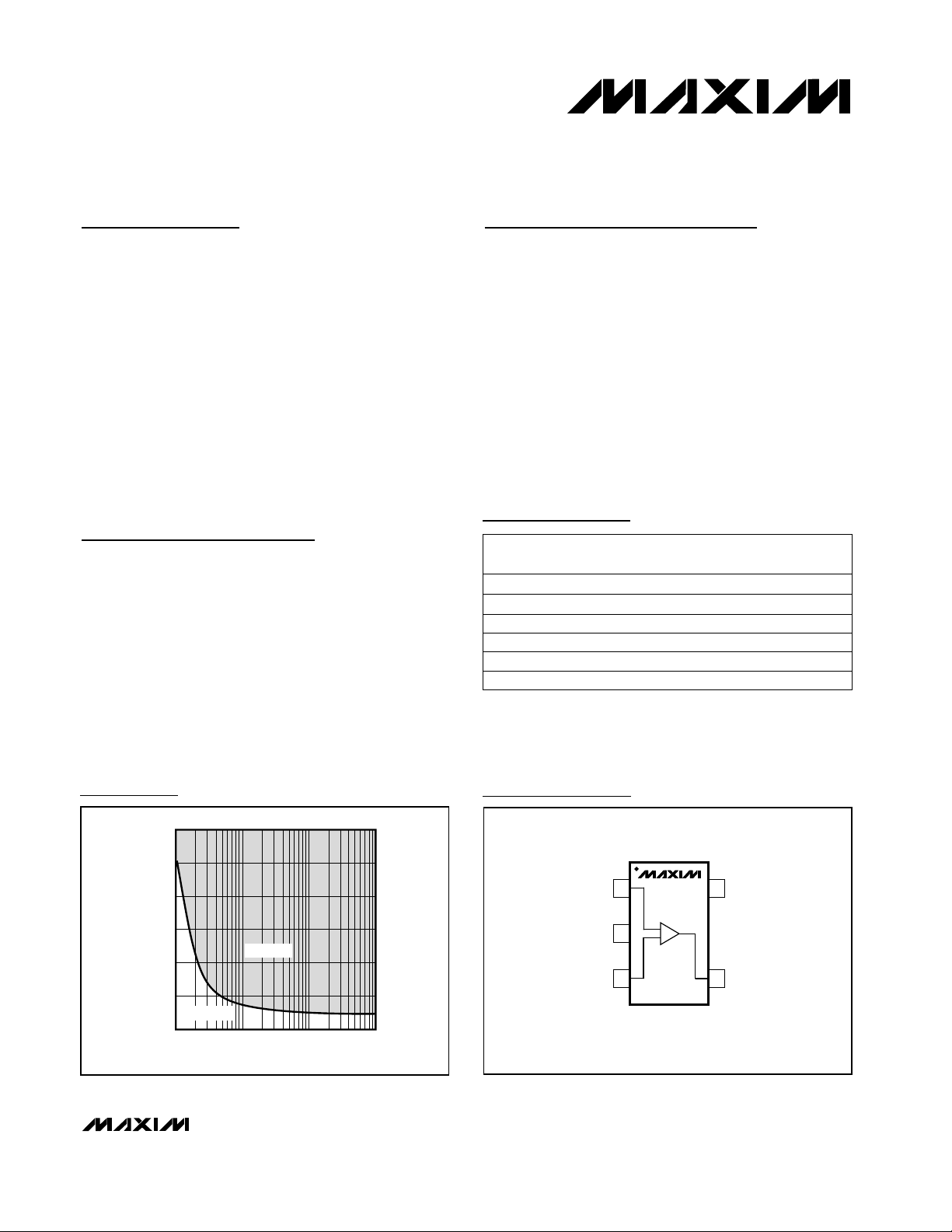
Capacitive-Load Stability
Ordering Information
Rail-to-Rail is a registered trademark of Nippon Motorola, Ltd.
MAX4492AUD
-40°C to +125°C 14 TSSOP
MAX4492ASD -40°C to +125°C 14 SO
TOP
MARK
AAB
ADKQ
AADB
—
—
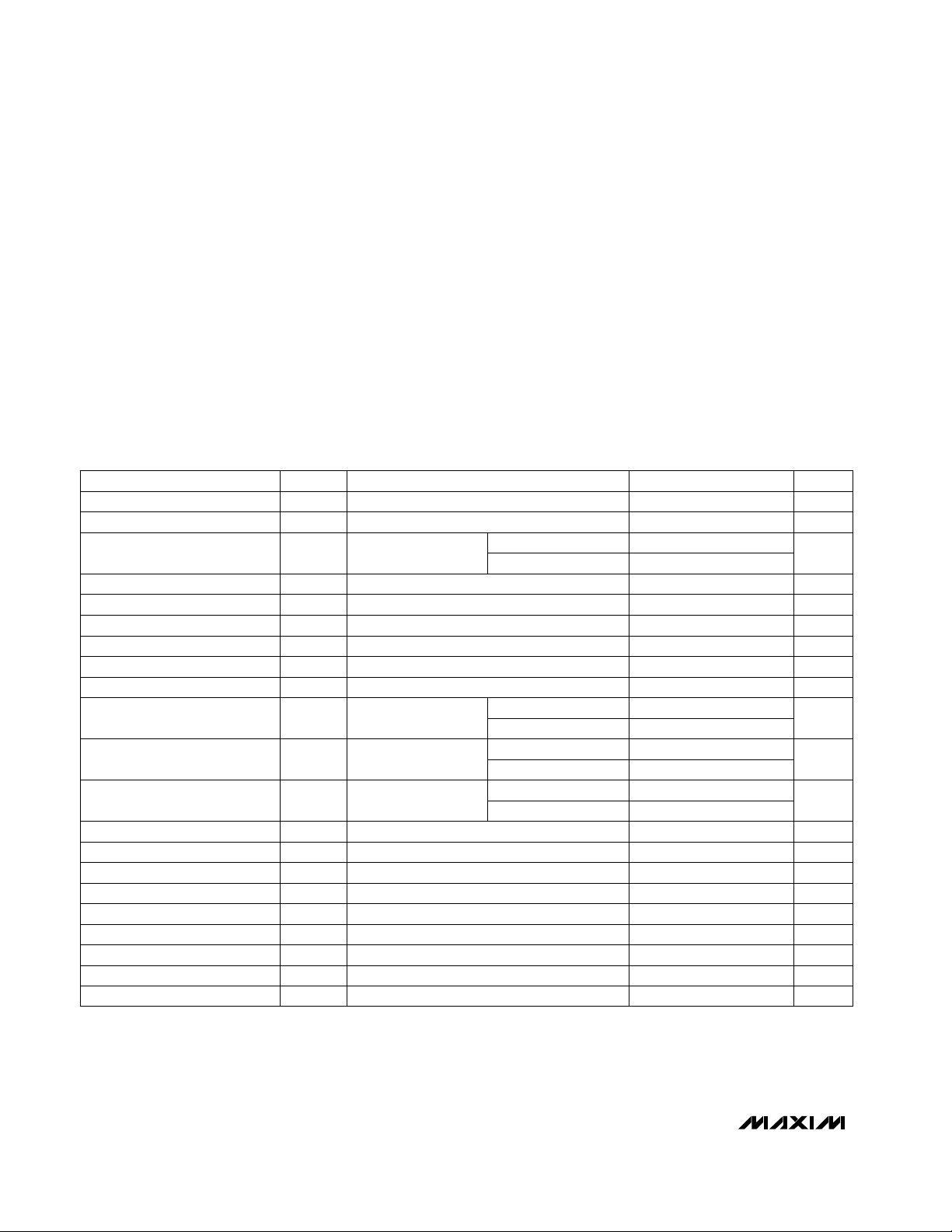
Pin Configurations/
Functional Diagrams
Pin Configurations continued at end of data sheet.
MAX4491AUA -40°C to +125°C 8 µMAX —
For pricing, delivery, and ordering information, please contact Maxim/Dallas Direct! at
1-888-629-4642, or visit Maxim’s website at www.maxim-ic.com.
6000
5000
4000
3000
2000
CAPACITIVE LOAD (pF)
1000
0
100 100k10k1k
UNSTABLE
STABLE
RESISTIVE LOAD (Ω)
TOP VIEW
MAX4490
15V
IN+
2
V
SS
- +
34
SOT23-5/SC70-5
DD
OUTIN-
MAX4490/MAX4491/MAX4492
Low-Cost, High-Slew-Rate,
Rail-to-Rail I/O Op Amps in SC70
2 _______________________________________________________________________________________
ABSOLUTE MAXIMUM RATINGS
ELECTRICAL CHARACTERISTICS
(VDD= 5V, VSS= 0, VCM= 0, V
OUT
= VDD/2, RL= 100kΩ connected to VDD/2, TA= T
MIN
to T
MAX
, unless otherwise noted. Typical
values are at T
A
= +25°C.) (Note 1)
Stresses beyond those listed under “Absolute Maximum Ratings” may cause permanent damage to the device. These are stress ratings only, and functional
operation of the device at these or any other conditions beyond those indicated in the operational sections of the specifications is not implied. Exposure to
absolute maximum rating conditions for extended periods may affect device reliability.
Supply Voltage (VDDto VSS)....................................................6V
All Other Pins ...................................(V
SS
- 0.3V) to (VDD+ 0.3V)
Output Short-Circuit Duration .................................................10s
Continuous Power Dissipation (T
A
= +70°C)
5-Pin SC70 (derate 2.5mW/°C above +70°C)............ 200mW
5-Pin SOT23 (derate 7.1mW/°C above +70°C).......... 571mW
8-Pin SOT23 (derate 5.26mW/°C above +70°C)........421 mW
8-Pin µMAX (derate 4.1mW/°C above +70°C) ........... 330mW
14-Pin TSSOP (derate 8.3mW/°C above +70°C) ....... 667mW
14-Pin SO (derate 8.3mW/°C above +70°C).............. 667mW
Operating Temperature Range ........................ -40°C to +125°C
Junction Temperature..................................................... +150°C
Storage Temperature Range ............................ -65°C to +150°C
Lead Temperature (soldering, 10s) ................................ +300°C
A
V(CL)
= 1, no sustained oscillations
ƒ = 10kHz
TA= +25°C
ƒ = 10kHz
Measured from 10% to 90% of 4V
P-P
step
(Note 2)
CL= 10pF
CL= 10pF
RL= 100kΩ
2.7V ≤ VDD≤ 5.5V
CL= 10pF
VSS≤ VCM≤ V
DD
Inferred from CMRR test
TA= T
MIN
to T
MAX
(Note 3)
(Note 3)
Sourcing or sinking
RL= 2kΩ
CONDITIONS
pF300Capacitive-Load Drive
fA√Hz
1i
n
Current-Noise Density
nV/√Hz
12e
n
Voltage-Noise Density
V/µs10SRSlew Rate
dB10Gain Margin
degrees60Phase Margin
pF5C
IN
Input Capacitance
MHz10GBWPGain-Bandwidth Product
mA±50I
OUT(SC)
Output Short-Circuit Current
65 85
mV
±1.5 ±10
V
OS
Input Offset Voltage
mA0.8 2I
S
V2.7 5.5V
DD
Supply Voltage Range
Supply Current (per amplifier)
dB
110
A
V
Large-Signal Voltage Gain
dB65 100PSRRPower-Supply Rejection Ratio
dB54 75CMRRCommon-Mode Rejection Ratio
VV
SS
V
DD
V
CM
Input Common-Mode Range
16
nA±0.05 ±2.5I
B
Input Bias Current
nA±0.05 ±2.5I
OS
Input Offset Current
MΩ
1000R
IN
Input Resistance
UNITSMIN TYP MAXSYMBOLPARAMETER
Note 1: All units production tested at TA= +25°C. Limits over temperature guaranteed by design.
Note 2: Guaranteed by the Power-Supply Rejection Ratio (PSRR) test.
Note 3: Input Offset Voltage, Input Bias Current, and Input Offset Current are all tested and guaranteed at both ends of the common-
mode range.
(V
SS
+ 0.25V) ≤ V
OUT
≤ (V
DD
- 0.25V)
RL= 100kΩ
RL= 2kΩ
55 200
mV
1.5
V
OH
Output-Voltage Swing High
Specified as
VDD- V
OH
RL= 100kΩ
RL= 2kΩ
35 150
mV
1.5
V
OL
Output-Voltage Swing Low
Specified as
VOL- V
SS
(Note 3)

MAX4490/MAX4491/MAX4492
Low-Cost, High-Slew-Rate,
Rail-to-Rail I/O Op Amps in SC70
_______________________________________________________________________________________ 3
5
MAX4490 toc02
Typical Operating Characteristics
(VDD= 5V, VSS= 0, VCM= VDD/2, RL= 100kΩ to VDD/2, TA= +25°C, unless otherwise noted.)
SUPPLY CURRENT PER AMPLIFIER
vs. TEMPERATURE
850
800
750
700
650
SUPPLY CURRENT (µA)
600
550
500
VDD = 5V
VDD = 2.7V
-40 -10 5 20-25 35 50 65 80 95 110 125
TEMPERATURE (°C)
OUTPUT SWING HIGH
vs. TEMPERATURE
80
70
60
50
(mV)
OUT
40
- V
DD
30
V
20
10
0
-40 -10 5 20 35-25 50 65 80 95 110 125
VDD = 5V
= 2kΩ
R
L
VDD = 5V OR 2.7V
= 100kΩ
R
L
TEMPERATURE (°C)
VDD = 2.7V
= 2kΩ
R
L
GAIN AND PHASE
vs. FREQUENCY (WITH C
60
50
40
30
20
GAIN (dB)
10
0
AV = 1000
-10
C
LOAD
-20
100 1k 10k 100k 1M 10M
PHASE
= 200pF
FREQUENCY (Hz)
GAIN
LOAD
MAX4490 toc07
MAX4490 toc 01
MAX4490 toc04
)
180
135
90
45
0
-45
PHASE (DEGREES)
-90
-135
-180
SUPPLY CURRENT PER AMPLIFIER
vs. SUPPLY VOLTAGE
1000
900
800
700
600
500
400
300
SUPPLY CURRENT (µA)
200
100
0
2.0 2.5 3.0 3.5 4.0 4.5 5.0 5.
SUPPLY VOLTAGE (V)
OUTPUT SWING LOW
vs. TEMPERATURE
80
70
60
50
(mV)
SS
40
- V
OUT
V
30
20
10
VDD = 5V OR 2.7V
= 100kΩ
R
L
0
-40 -10 5 20 35-25 50 65 80 95 110 125
VDD = 5V
= 2kΩ
R
L
TEMPERATURE (°C)
VDD = 2.7V
R
LARGE-SIGNAL GAIN
vs. TEMPERATURE
130
120
110
100
LARGE-SIGNAL GAIN (dB)
90
80
-40 -10 5-25 20 35 50 65 80 95 110 125
TEMPERATURE (°C)
= 2kΩ
L
VDD = 5V
-0.2
-0.4
-0.6
-0.8
-1.0
-1.2
OFFSET VOLTAGE (mV)
-1.4
-1.6
-1.8
-2.0
MAX4490 toc05
GAIN (dB)
MAX4490 toc08
PSSR (dB)
-100
INPUT OFFSET VOLTAGE
vs. TEMPERATURE
0
-40 -25 -10 5 20 35 50 8065 95 125110
TEMPERATURE (°C)
OP AMP GAIN AND PHASE
vs. FREQUENCY
60
50
40
30
20
10
0
-10
-20
AV = 1000
= 10pF
C
L
100 1k
PHASE
10k
FREQUENCY (Hz)
GAIN
100k 1M 10M
POWER-SUPPLY REJECTION RATIO
vs. FREQUENCY
0
AV = 1
-10
-20
-30
-40
-50
-60
-70
-80
-90
10 1k 10k100 100k 1M 10M
FREQUENCY (Hz)
MAX4490 toc06
MAX4490 toc03
180
135
90
45
0
-45
PHASE (DEGREES)
-90
-135
-180
MAX4490 toc09

MAX4490/MAX4491/MAX4492
Low-Cost, High-Slew-Rate,
Rail-to-Rail I/O Op Amps in SC70
4 _______________________________________________________________________________________
Typical Operating Characteristics (continued)
(VDD= 5V, VSS= 0, VCM= VDD/2, RL= 100kΩ to VDD/2, TA= +25°C, unless otherwise noted.)
0.01
1
0.1
10
100
1k
1k 10k100 100k 1M 10M
OUTPUT IMPEDANCE vs. FREQUENCY
MAX4490 toc10
FREQUENCY (Hz)
OUTPUT IMPEDANCE (Ω)
AV = 1
0.040
0
10 100 1k 10k 100k
TOTAL HARMONIC DISTORTION PLUS
NOISE vs. FREQUENCY
0.005
0.010
MAX4490 toc11
FREQUENCY (Hz)
THD + NOISE (%)
0.015
0.020
0.025
0.030
0.035
AV = 1V/V
2Vp-p SIGNAL
500kHz LOWPASS FILTER
RL = 2kΩ
RL = 10kΩ
LARGE-SIGNAL TRANSIENT RESPONSE
(NONINVERTING)
AV = 1
IN
OUT
40µs/div
MAX4490toc12
LARGE-SIGNAL TRANSIENT RESPONSE
(INVERTING)
AV = -1
IN
OUT
2V/div
2V/div
40µs/div
MAX4490toc13
SMALL-SIGNAL TRANSIENT RESPONSE
(NONINVERTING)
AV = 1
40µs/div
IN
OUT
50mV/div
50mV/div
MAX4490toc14
SMALL-SIGNAL TRANSIENT RESPONSE
(INVERTING)
AV = -1
IN
OUT
40µs/div
MAX4490toc15
50mV/div
50mV/div
POWER-UP TRANSIENT RESPONSE
AV = 1, VIN CONNECTED TO VDD/2, RL = 2kΩ
V
DD
OUT
2V/div
1V/div
MAX4490toc16
4µs/div
0
4
2
8
6
10
12
2.5 3.5 4.03.0 4.5 5.0 5.5
SLEW RATE vs. SUPPLY VOLTAGE
MAX4490 toc17
SUPPLY VOLTAGE (V)
SLEW RATE (V/µS)
AV = 1
10% TO 90% STEP
0
-20
-40
-120
0.001 1 10 1000.01 0.1 1000
MAX4491/MAX4492
CROSSTALK vs. FREQUENCY
-60
-80
-100
MAX4492toc18
FREQUENCY (MHz)
CROSSTALK (dB)

MAX4490/MAX4491/MAX4492
Low-Cost, High-Slew-Rate,
Rail-to-Rail I/O Op Amps in SC70
_______________________________________________________________________________________ 5
NAME FUNCTION
MAX4490
1 IN+ Noninverting Input
PIN
2 V
SS
Negative Supply Input. Connect to ground for single-supply operation.
3 IN- Inverting Input
— INA- Inverting Input to Amplifier A
— INA+ Noninverting Input to Amplifier A
5 V
DD
Positive Supply Input
4 OUT Amplifier Output
— INC+, IND+ Noninverting Inputs to Amplifiers C and D
— OUTB Amplifier B Output
— INB- Inverting Input to Amplifier B
— INB+ Noninverting Input to Amplifier B
— OUTA Amplifier A Output
Pin Description
MAX4492
—
11
—
2
3
4
—
10, 12
7
6
5
1
MAX4491
—
4
—
2
3
8
—
—
7
6
5
1
— — 9, 13 INC-, IND- Inverting Inputs to Amplifiers C and D
— — 8, 14 OUTC, OUTD Amplifiers C and D Outputs
Detailed Description
Rail-to-Rail Input Stage
The MAX4490/MAX4491/MAX4492 CMOS operational
amplifiers have parallel-connected N- and P-channel
differential input stages that combine to accept a common-mode range extending to both supply rails. The Nchannel stage is active for common-mode input
voltages typically greater than (VSS+ 1.2V), and the Pchannel stage is active for common-mode input voltages typically less than (VDD- 1.2V).
Rail-to-Rail Output Stage
The MAX4490/MAX4491/MAX4492 CMOS operational
amplifiers feature class-AB push-pull output stages that
can drive a 100kΩ load to within 1.5mV of either supply
rail. Short-circuit output current is typically ±50mA.
Figures 1a and 1b show the typical temperature dependence of output source and sink currents, respectively,
for three fixed values of (VDD- VOH) and (VOL- VSS).
For example, at VDD= 5.0V, the load currents that maintain (VDD- VOH) = 100mV and (VOL- VSS) = 100mV at
TA= +25°C are 2.2mA and 3.3mA, respectively, when
the load is connected to VDD/2. Consistent resistivedrive capability is (2.5 - 0.1) / 2.2 = 1.1kΩ. For the same
application, resistive-drive capability is 2.2kΩ when the
load is connected to VDDor VSS.
Applications Information
Power-Supply Considerations
The MAX4490/MAX4491/MAX4492 operate from a single 2.7V to 5.5V supply or from dual ±1.35V to ±2.75V
supplies with typically 800µA supply current per amplifier. A high power-supply rejection ratio of 100dB
allows for extended operation from a decaying battery
voltage, thereby simplifying designs for portable applications. For single-supply operation, bypass the power
supply with a 0.1µF ceramic capacitor placed close to
the VDDpin. For dual-supply operation, bypass each
supply to ground.
Input Capacitance
One consequence of the parallel-connected differential
input stages for rail-to-rail operation is a relatively large
input capacitance CIN(typically 5pF). This introduces a

pole at frequency (2πR′CIN)-1, where R′ is the parallel
combination of the gain-setting resistors for the inverting or noninverting amplifier configuration (Figure 2). If
the pole frequency is less than or comparable to the
unity-gain bandwidth (10MHz), the phase margin will
be reduced, and the amplifier will exhibit degraded
AC performance through either ringing in the step
response or sustained oscillations. The pole frequency is
10MHz when R′ = 3.2kΩ. To maximize stability, R′ <3kΩ
is recommended.
Applications that require rail-to-rail operation with minimal loading (for small VDD- VOHand VOL- VSS) will
typically require R′ values >3kΩ. To improve step
response under these conditions, connect a small
capacitor Cfbetween the inverting input and output.
Choose Cfas follows:
Cf= 5(R / Rf) [pf]
where Rfis the feedback resistor and R is the gain-setting resistor (Figure 2).
Figure 3 shows the step response for a noninverting
amplifier subject to R′ = 4kΩ with and without the C
f
feedback capacitor.
MAX4490/MAX4491/MAX4492
Low-Cost, High-Slew-Rate,
Rail-to-Rail I/O Op Amps in SC70
6 _______________________________________________________________________________________
Figure 1a. Output Source Current vs. Temperature
Figure 1b. Output Sink Current vs. Temperature
Figure 2. Inverting and Noninverting Amplifier with Feedback
Compensation
6
5
VDD = 2.7V
4
3
2
OUTPUT SOURCE CURRENT (mA)
1
0
-40 -10-25 5 20 35 50 65 80 12595 110
TEMPERATURE (
VDD - VOH = 200mV
- VOH = 100mV
V
DD
- VOH = 50mV
V
DD
VDD = 5V
°C)
INVERTING
V
IN
R
C
R
MAX4490
f
f
V
OUT
R′ = R || R
f
RfCf = RC
IN
9
8
7
6
5
4
3
OUTPUT SINK CURRENT (mA)
2
1
0
VDD = 2.7V
-40 -10-25 5 20 35 6550 80 11095 125
TEMPERATURE (°C)
VDD - VOH = 200mV
- VOH = 100mV
V
DD
- VOH = 50mV
V
DD
VDD = 5V
NONINVERTING
R
V
IN
MAX4490
R
f
C
f
R′ = R || R
RfCf = RC
V
OUT
f
IN

Driving Capacitive Loads
In conjunction with op amp output resistance, capacitive loads introduce a pole frequency that can reduce
phase margin and lead to unstable operation. The
MAX4490/MAX4491/MAX4492 drive capacitive loads
up to 300pF without significant degradation of step
response and slew rate (Figure 4). Capacitive-Load
Stability (page 1) shows regions of stable and marginally stable (step overshoot <10%) operation for different
combinations of capacitive and resistive loads.
Improve stability for large capacitive loads by adding
an isolation resistor (typically 10Ω) in series with the
output (Figure 5). Note that the isolation resistor forms a
voltage divider with potential for gain error.
Chip Information
MAX4490 TRANSISTOR COUNT: 60
MAX4491 TRANSISTOR COUNT: 120
MAX4492 TRANSISTOR COUNT: 240
SUBSTRATE CONNECTED TO V
SS
MAX4490/MAX4491/MAX4492
Low-Cost, High-Slew-Rate,
Rail-to-Rail I/O Op Amps in SC70
_______________________________________________________________________________________ 7
Figure 4. Step Response With and Without Capacitive Loading
Figure 3. Step Response With and Without Feedback
Compensation
3a)
WITHOUT FEEDBACK COMPENSATION
AV = -1, RL = 4kΩ, Cf = 0
4a)
WITHOUT CAPACITIVE LOADING
AV = +1, RL = 100kΩ, CL = 0
3b)
WITH FEEDBACK COMPENSATION
AV = -1, RL = 4kΩ, Cf = 5pF
4b)
WITH CAPACITIVE LOADING
AV = +1, RL = 100kΩ, CL = 300pF

MAX4490/MAX4491/MAX4492
Low-Cost, High-Slew-Rate,
Rail-to-Rail I/O Op Amps in SC70
Maxim cannot assume responsibility for use of any circuitry other than circuitry entirely embodied in a Maxim product. No circuit patent licenses are
implied. Maxim reserves the right to change the circuitry and specifications without notice at any time.
8 _____________________Maxim Integrated Products, 120 San Gabriel Drive, Sunnyvale, CA 94086 408-737-7600
© 2001 Maxim Integrated Products Printed USA is a registered trademark of Maxim Integrated Products.
Figure 5. Isolation Resistor for Large Capacitive Loads
Package Information
Pin Configurations/
Functional Diagrams (continued)
TOP VIEW
V
IN
OUTA
INA-
INA+
SS
MAX4490
R
S
C
V
LOAD
OUT
1
MAX4491
+ -
2
3
4
+ -
SOT23-8/µMAX
1
OUTA
2
V
DD
OUTB
INB-
INB+V
INA-
INA+
V
INB+
INB-
3
4
DD
5
6
7
8
7
6
5
+ -
MAX4492
+ -
+ -
+ -
OUTD
14
IND-
13
IND+
12
V
11
10
INC+
9
INC-
8
OUTCOUTB
TSSOP/SO
SC70, 5L.EPS
SS
 Loading...