

For free samples & the latest literature: http://www.maxim-ic.com, or phone 1-800-998-8800.
For small orders, phone 1-800-835-8769.
General Description
The MAX408/428/448 are high speed general purpose
monolithic operational amplifiers in a single, dual or
quad package, that are useful for signal frequencies
extending into the video range. These Op Amps function in gain configurations greater-than or equal-to 3.
High output current allows large capacitive loads to be
driven at high speeds.
Open-loop voltage gain of 10k V/V and high slew rate of
90V/µs make the MAX408/428/448 ideal for analog
amplification and high speed signal processing. 100MHz
gain bandwidth and a ±0.1% settling time of l50ns make
each amplifier ideal for fast data conversion systems.
The amplifiers are capable of driving back terminated
transmission lines of 75Ω with amplitudes of 5V peakto-peak.
Along with the high speed and output drive capability,
a 35nA offset current and trimmable offset voltage
make the MAX408/428/448 optimal for signal conditioning applications where accuracy must be maintained.
Applications
Video Amplifiers
Test Equipment
Waveform Generators
Video Distribution
Pulse Amplifiers
Features
♦ Fast Settling Time: ±0.1% In 150ns
♦ High Slew Rate: 90V/µs
♦ Large Gain Bandwidth: 100MHz
♦ Full Power Bandwidth: 4.8MHz at 6V p-p
♦ Ease of Use: Internally Compensated for
A
CL
≥ 3 with 50°–60° Phase Margin
♦ Low Supply Voltage Operation: ±4V
♦ Wide Input Voltage Range: Within 1.5V of V+ and
0.5V of V-
♦ Minimal Crosstalk: >90dB Separation
(MAX428/448)
♦ Short Circuit Protection
MAX408/428/448
Single/Dual/Quad High-Speed, Fast-Settling,
High Output Current Operational Amplifier
________________________________________________________________
Maxim Integrated Products
1
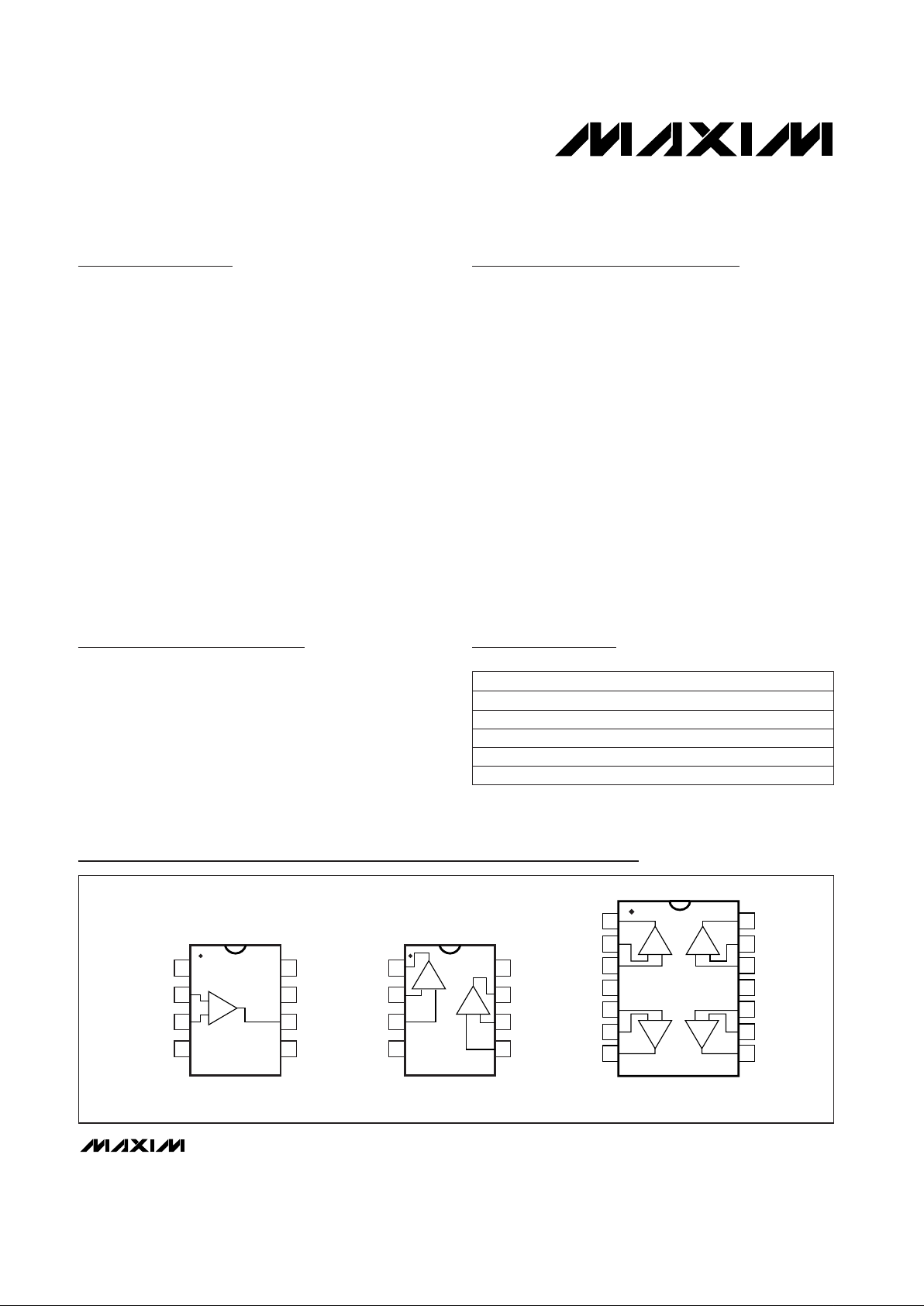
OUT
BALANCEV-
1
2
87N.C.
V+-IN
+IN
+
-
BALANCE
DIP/SO
TOP VIEW
3
4
6
5
MAX408
-IN
B
+IN
B
V-
1
2
87V+
OUT2-IN
A
+IN
A
+
-
+
-
OUT 1
DIP/SO
3
4
6
5
MAX428
14
13
12
11
10
9
8
1
2
3
4
5
6
7
OUT
D
-IN
D
+IN
D
V-V+
+IN
A
-IN
A
OUTA
MAX448
+IN
C
-IN
C
OUT
C
OUT
B
-IN
B
+IN
B
DIP/SO
A
B
+
-
A
+
-
C
+
-
B
+
-
D
19-2394; Rev 1; 7/97
PART
MAX408ACPA
MAX408ACSA
MAX408CPA 0°C to +70°C
0°C to +70°C
0°C to +70°C
TEMP. RANGE PIN-PACKAGE
8 Lead Plastic DIP
8 Lead Small Outline
8 Lead Plastic DIP
Ordering Information continued at end of data sheet.
Pin Configurations
Ordering Information
MAX408CSA 0°C to +70°C 8 Lead Small Outline
MAX408C/D 0°C to +70°C Dice
MAX408/428/448
Single/Dual/Quad High-Speed, Fast-Settling,
High Output Current Operational Amplifier
2 _______________________________________________________________________________________
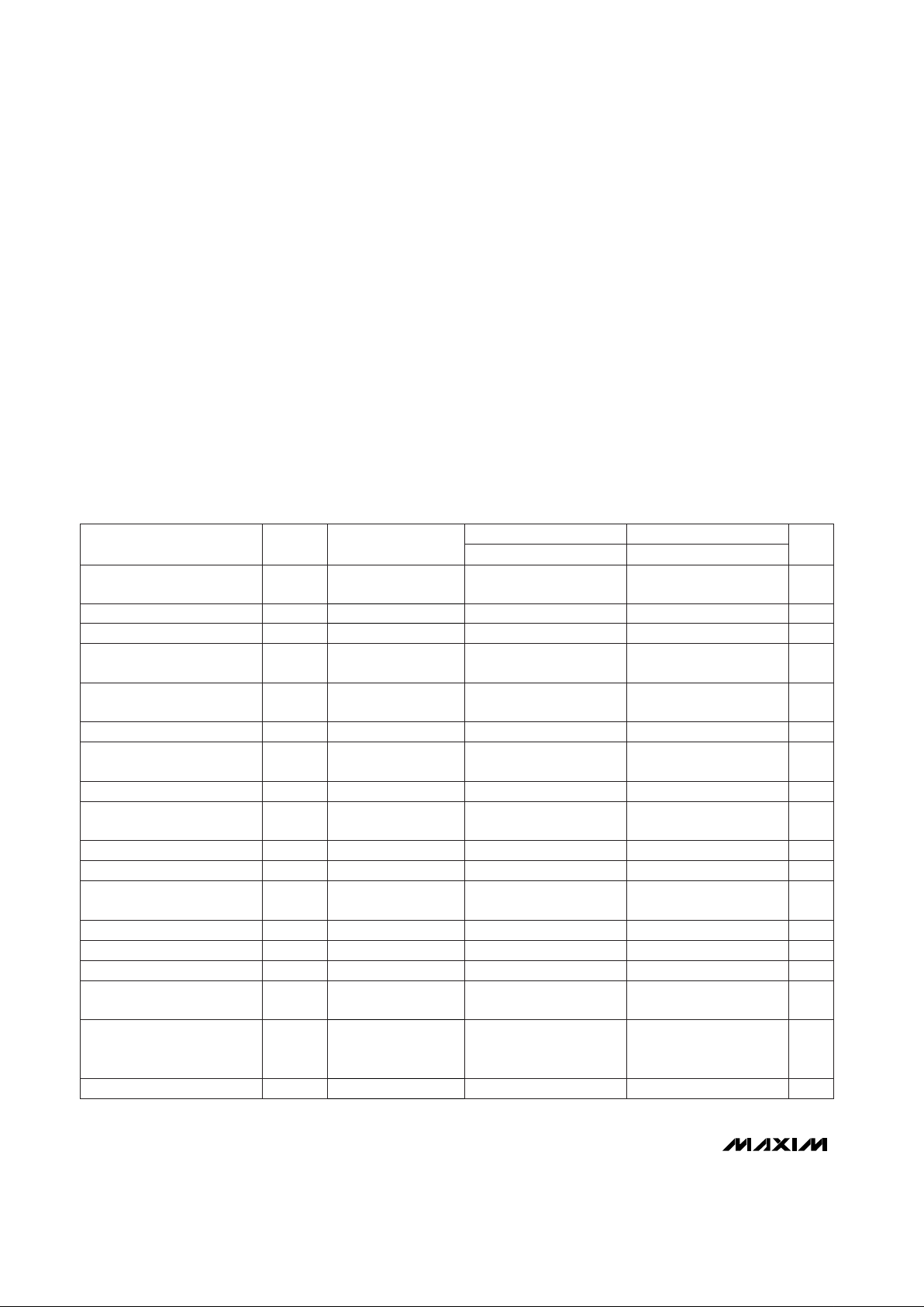
ABSOLUTE MAXIMUM RATINGS
ELECTRICAL CHARACTERISTICS—MAX408
(VS= ±5V, TA= +25°C, unless otherwise noted.)
Stresses beyond those listed under “Absolute Maximum Ratings” may cause permanent damage to the device. These are stress ratings only, and functional
operation of the device at these or any other conditions beyond those indicated in the operational sections of the specifications is not implied. Exposure to
absolute maximum rating conditions for extended periods may affect device reliability.
Note 1: Not tested, guaranteed by design.
Supply Voltages.....................................................................+6V
Differential Input Voltage .......................................................+9V
Common Mode Input Voltage .......................................|Vs| -0.5V
Output Short Circuit Current Duration ...........................Indefinite
Continuous Power Dissipation (T
A
= +70°C)
8-Pin Plastic DIP (derate 9.09mW/°C above +70°C) ....727mW
8-Pin SO (derate 5.88mW/°C above +70°C).................471mW
14-Pin Plastic DIP
(derate 10.00mW/°C above +70°C).........................800mW
14-Pin SO (derate 8.33mW/°C above +70°C)...............667mW
Operating Temperature Range
Commercial (MAX4_8AC/C) ................................0°C to +70°C
Storage Temperature Range.............................-65°C to +150°C
Lead Temperature (Soldering, 60 seconds)...................+300° C
0°C ≤ TA≤ 70°C
TA= 25°C
0°C ≤ TA≤ 70°C
To ±0.1% (±4mV) of
Final Value (Figure 1)
(Note 1)
10–90% of Leading
Edge (Figure 1)
V
OUT
= ±3V,RL= 2kΩ
BW = 10Hz to 100kHz
∆VPS= ±0.5V
VCM= ±2V
TA= 25°C
0°C ≤ TA≤ 70°C
(Note 1)
(Note 1)
RL= 2kΩ
R
L
= 150Ω
CONDITIONS
MHz100GBWGain Bandwidth Product
ns150 200t
S
Settling Time
V/µS60 90SRSlew Rate (Note 1)
dB60 66PSRRPower Supply Rejection Ratio
dB60 70CMRRCommonMode RejectionRatio
mA710I
S
Power Supply Current
V
±3.5
±2.0 ±2.4
V
OUT
Output Voltage Swing
nA650 1100I
B
Input Bias Current
µV/°C20
∆VOS/∆T
mV
512
816
V
OS
Input Offset Voltage
Average Offset Voltage Drift
V/mV25A
V
Open Loop Voltage Gain
µV
RMS
12e
N
Input Voltage Noise
pF3C
INC
Common Mode Input
Capacitance
pF2C
IND
Differential Input Capacitance
nA
35 120
70 200
I
OS
Input Offset Current
V
+3 +3.5
-4 -4.5
V
CM
Input Common Mode Range
MΩ
310R
IND
Differential Input Resistance
MΩ
48R
INC
Common Mode Input
Resistance
UNITS
MAX408C
SYMBOLPARAMETER
100
150 200
60 90
60 66
60 70
710
±3.5
±2.5 ±2.7
650 1100
20
36
510
510
12
3
2
35 120
70 200
+3 +3.5
-4 -4.5
310
48
MAX408AC
MIN TYP MAX MIN TYP MAX
MAX408/428/448
Single/Dual/Quad High-Speed, Fast-Settling,
High Output Current Operational Amplifier
_______________________________________________________________________________________ 3
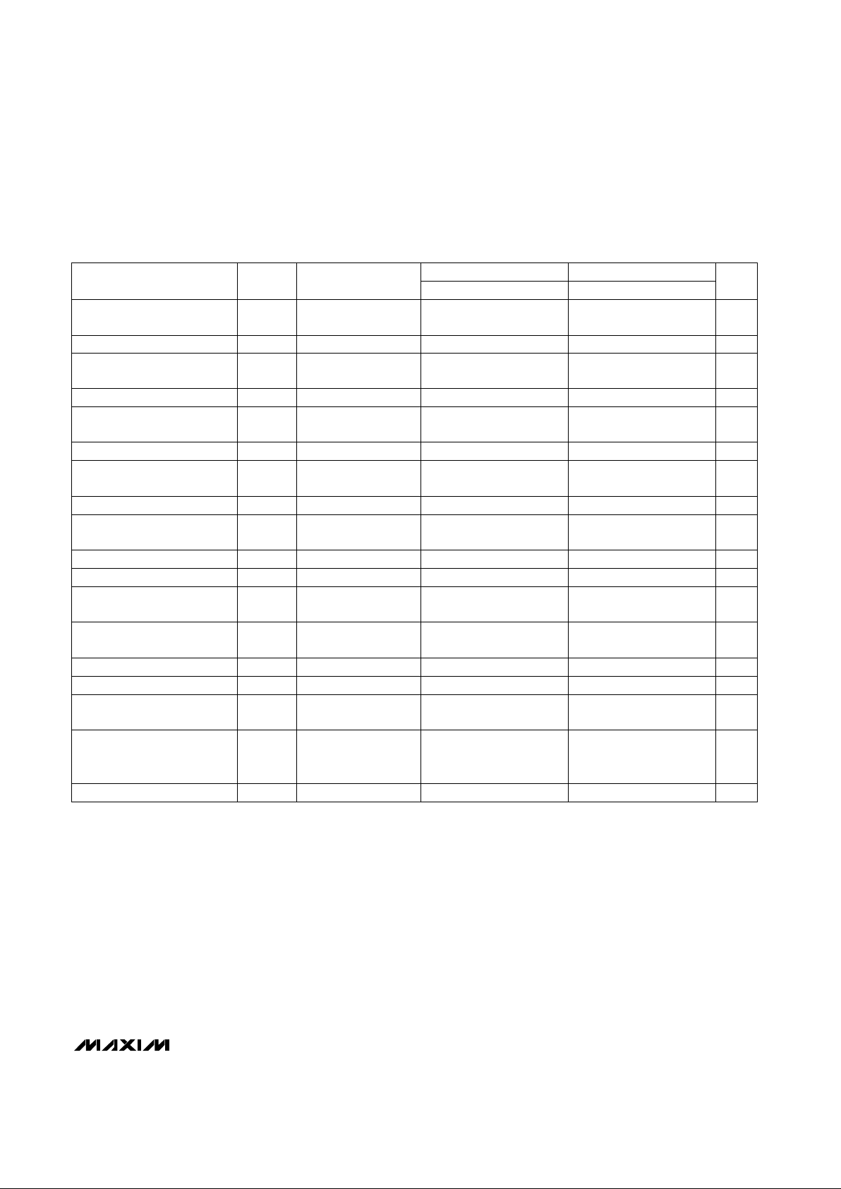
ELECTRICAL CHARACTERISTICS—MAX428
(VS= ±5V, TA= +25°C, unless otherwise noted.)
TA= 25°C
0°C ≤ TA≤ 70°C
0°C ≤ TA≤ 70°C
TA= 25°C
0°C ≤ TA≤ 70°C
To ±0.1% (±4mV) of
Final Value (Figure 1)
(Note 1)
10–90% of Leading
Edge (Figure 1)
V
OUT
= ±3V,RL= 2kΩ
BW = 10Hz to 100kHz
∆VPS= ±0.5V
VCM= ±2V
(Note 1)
(Note 1)
RL= 2kΩ
R
L
= 150Ω
CONDITIONS
MHz100GBWGain Bandwidth Product
ns150 200t
S
Settling Time
V/µS60 90SRSlew Rate (Note 1)
dB60 66PSRRPower Supply Rejection Ratio
dB60 70CMRRCommonMode RejectionRatio
mA15 20I
S
Power Supply Current
(Both Amplifiers)
V
±3.5
±2.0 ±2.4
V
OUT
Output Voltage Swing
mA
650 1100
1700
I
B
Input Bias Current
µV/°C20
∆VOS/∆T
mV
512
816
V
OS
Input Offset Voltage
Average Offset Voltage Drift
V/mV25A
V
Open Loop Voltage Gain
µV
RMS
12e
N
Input Voltage Noise
pF3C
INC
Common Mode Input
Capacitance
pF2C
IND
Differential Input Capacitance
nA35 120I
OS
Input Offset Current
V
+3 +3.5
-4 -4.5
V
CM
Input Common Mode Range
MΩ
310R
IND
Differential Input Resistance
MΩ
48R
INC
Common Mode Input
Resistance
UNITS
MAX428C
SYMBOLPARAMETER
100
150 200
60 90
60 66
60 70
15 20
±3.5
±2.5 ±2.7
650 1100
1700
20
36
510
510
12
3
2
35 120
+3 +3.5
-4 -4.5
310
48
MAX428AC
MIN TYP MAX MIN TYP MAX
Note 1: Not tested, guaranteed by design.
MAX408/428/448
Single/Dual/Quad High-Speed, Fast-Settling,
High Output Current Operational Amplifier
4 _______________________________________________________________________________________
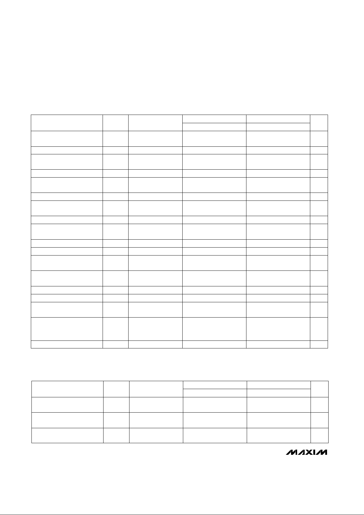
ELECTRICAL CHARACTERISTICS—MAX448
(VS= ±5V, TA= +25°C, unless otherwise noted.)
Note 1: Not tested, guaranteed by design.
AC CHARACTERISTICS—MAX408/428/448
(VS= ±5V, TA= +25°C, unless otherwise specified.)
MIN TYP MAXMIN TYP MAX
MAX408AC
48
310
+3 +3.5
-4 -4.5
35 120
3
12
410
36
510
20
650 1100
1700
±3.5
±2.5 ±2.7
30 40
60 66
60 70
60 90
150 200
100
PARAMETER SYMBOL
MAX408C
UNITS
Common Mode Input
Resistance
R
INC
48
MΩ
Differential Input Resistance R
IND
310
MΩ
Input Common Mode Range V
CM
+3 +3.5
-4 -4.5
V
Input Offset Current I
OS
35 120 nA
Differential Input Capacitance C
IND
2 pF
Common Mode Input
Capacitance
C
INC
3 pF
Input Voltage Noise e
N
12 µV
RMS
Open Loop Voltage Gain A
V
25 V/mV
Average Offset Voltage Drift
Input Offset Voltage V
OS
512
816
mV
∆VOS/∆T
20 µV/°C
Input Bias Current I
B
650 1100
1700
nA
Output Voltage Swing V
OUT
±3.5
±2.0 ±2.4
V
Power Supply Current
(All Four Amplifiers)
I
S
30 40 mA
Power Supply Rejection Ratio PSRR 60 66 dB
Common Mode Rejection Ratio CMRR 60 70 dB
Slew Rate (Note 1) SR 60 90 V/µS
Settling Time t
S
150 200 ns
Gain Bandwidth Product GBW 100 MHz
CONDITIONS
RL= 2kΩ
R
L
= 150Ω
(Note 1)
(Note 1)
∆VPS= ±0.5V
VCM= ±2V
BW = 10Hz to 100kHz
V
OUT
= ±3V,RL= 2kΩ
10–90% of Leading
Edge (Figure 1)
To ±0.1% (±4mV) of
Final Value (Figure 1)
(Note 1)
TA= 25°C
0°C ≤ TA≤ 70°C
0°C < TA≤ 70°C
TA= 25°C
0°C ≤ TA≤ 70°C
MIN TYP MAXMIN TYP MAX
MAX4XXC
7
4.8
-96
PARAMETER SYMBOL
MAX4XXC
UNITS
Full Power Bandwidth
Small Signal Rise/Fall Time tr/tf 7 ns
BW
FP
4.8 MHz
Amp-Amp Crosstalk
(MAX428/448)
-96 dB
CONDITIONS
eO= ±100mV
10–90% (Figure 1)
RL= 2kΩ, CL= 50pF
V
OUT
= 6Vp-p
Input Referenced
f = 10kHz

MAX408/428/448
Single/Dual/Quad High-Speed, Fast-Settling,
High Output Current Operational Amplifier
_______________________________________________________________________________________
5
200
400
600
800
1000
1200
0 10203040506070
INPUT BIAS CURRENT
vs. TEMPERATURE
MAX408-01
TEMPERATURE (°C)
INPUT BIAS CURRENT (nA)
-10
-5
0
5
10
0 10203040506070
NORMALIZED OPEN LOOP GAIN
vs. TEMPERATURE
MAX408-02
TEMPERATURE (°C)
NORMALIZED OPEN LOOP GAIN (dB)
2
4
6
8
10
3456
SUPPLY CURRENT
vs. SUPPLY VOLTAGE
MAX408-03
SUPPLY VOLTAGE (±V)
SUPPLY CURRENT (mA)
50
60
70
80
90
3456
OPEN LOOP GAIN
vs. SUPPLY VOLTAGE
MAX408-04
SUPPLY VOLTAGE (±V)
GAIN (dB)
5
0
10Ω 100Ω 1kΩ
MAXIMUM OUTPUT VOLTAGE SWING
vs. LOAD RESISTANCE
1
MAX408-07
LOAD RESISTANCE (Ω)
VOLTAGE SWING (V)
2
3
4
NEGATIVE SWING
POSITIVE SWING
20
40
60
80
100
0 10203040506070
INPUT OFFSET CURRENT
vs. TEMPERATURE
MAX408-05
TEMPERATURE (°C)
INPUT OFFSET CURRENT (nA)
-20
-120
1k 10k 100k 1M 10M 100M
AMPLIFIER/AMPLIFIER CROSSTALK
vs. FREQUENCY (MAX428/448)
-100
MAX408-06
FREQUENCY (Hz)
CROSSTALK (dB)
-80
-60
-40
0
2
4
6
8
0 10203040506070
MAXIMUM OUTPUT VOLTAGE SWING
vs. TEMPERATURE
MAX408-08
TEMPERATURE (°C)
P-P VOLTAGE SWING (V)
RL = 2kΩ
RL = 50Ω
Typical Operating Characteristics
(VS= ±5, TA = +25°C, unless otherwise stated and apply for each individual op amp where applicable.)

MAX408/428/448
Single/Dual/Quad High-Speed, Fast-Settling,
High Output Current Operational Amplifier
6 _______________________________________________________________________________________
Typical Operating Characteristics
(TA = +25°C, unless otherwise noted.)
20
40
60
80
100
120
0 10203040506070
SHORT CURCUIT OUTPUT CURRENT
vs. TEMPERATURE
MAX408-09
TEMPERATURE (°C)
SHORT CIRCUIT OUTPUT CURRENT (mA)
-I
SC
+I
SC
100 10k 100k1k 1M
EQUIVALENT INPUT NOISE
vs. BANDWIDTH
MAX408-10
BANDWIDTH (Hz)
(LOWER - 3dB FREQUENCY = 10Hz)
EQUIVALENT INPUT NOISE (µV)
100
0.1
1
10
R
SOURCE
= 10kΩ
THERMAL NOISE OF
10kΩ RESISTOR
R
SOURCE
= 0
-40
-20
0
1kHz 1MHz 10MHz 100MHz10kHz 100kHz 1GHz
OPEN LOOP FREQUENCY RESPONSE
20
40
60
80
360
300
240
180
120
60
0
MAX408toc11
FREQUENCY
OPEN LOOP GAIN (A
V
, dB)
PHASE (φ, DGREES)
Av
RL = 2kΩ
C
L
= 5pF
10dB
GAIN MARGIN = G
M
10dB
PHASE
MARGIN = φ
M
φ
-20
-15
-10
-5
0
5
10
15
20
25
30
35
360
300
240
180
120
60
0
1M 1G100M10M
OPEN LOOP FREQUENCY RESPONSE,
R
L
= 2kΩ, CL = 50pF
MAX408-13
FREQUENCY (Hz)
OPEN LOOP GAIN (Av, dB)
PHASE (φ, DEGREES)
Av
φ
-20
-15
-10
-5
0
5
10
15
20
25
30
35
360
300
240
180
120
60
0
1M 1G100M10M
OPEN LOOP FREQUENCY RESPONSE,
R
L
= 50Ω, CL = 50pF
MAX408-12
FREQUENCY (Hz)
OPEN LOOP GAIN (Av, dB)
PHASE (φ, DEGREES)
Av
φ
50
45
30
55 25
40
35
0604020 80
10dB PHASE MARGIN AND
10dB FREQUENCY vs. TEMP
MAX408toc14
TEMPERATURE (°C)
10dB PHASE MARGIN (φ
M
, DEGREES)
10dB FREQUENCY (MHz)
φ
M
10dB FREQUENCY
R
L
= 2kΩ
C
L
= 50pF
540
4
60
650
80
70
0604020 80
GAIN MARGIN AND 180 DEGREE
FREQUENCY vs. TEMP (A
V
= 10dB)
MAX408toc15
TEMPERATURE (°C)
GAIN MARGIN (G
M
, dB)
180 DEGREE FREQUENCY (MHz)
G
M
180 FREQUENCY
RL = 2kΩ
C
L
= 50pF

___________Application Information
AC Characteristics
The 35MHz 10dB crossover point of the MAX408/
428/448 is achieved without feed forward compensation, a technique which can produce long tails in the
recovery characteristic. The single pole rolloff follows
the classic 20dB/decade slope to frequencies
approaching 50MHz. The 10dB (3.2V/V) phase margin
of 50°, even with a capacitive load of 50pF, gives stable
and predictable performance down to non-inverting
gain configurations of approximately 3V/V (inverting
gains of -2V/V). At frequencies beyond 50MHz, the
20dB/decade slope is disturbed by an output stage
zero, the damping factor of which is dependent upon
the RL, CLload combination. This results in loss of gain
MAX408/428/448
Single/Dual/Quad High-Speed, Fast-Settling,
High Output Current Operational Amplifier
_______________________________________________________________________________________ 7
e
IN
1kΩ
2kΩ
2kΩ
300Ω
150Ω
e
S = SETTLE VOLTAGE
R
L
+1V
-1V
2V
±4mV OF
FINAL VALUE
SETTLING
TIME
-2V
10%
SLEW RATE
90%
C
L
10pF
e
O
e
IN
e
OUT
e
o
e
o
e
s
e
IN
OV
OV
OV
OV
Figure 1A. Settling Time and Slew Rate Test Circuit
Figure 1B. Large Signal Response
Figure 1C. Small Signal Response
Note that to properly measure e
s
, amplifier and settle resistor ratios should be matched to 0.5% and probe capacitance ≤35pF

MAX408/428/448
margin (gain at loop phase = 360°) at frequencies of 70
to 100MHz which at a gain margin of 5dB (RL= 2k, C
L
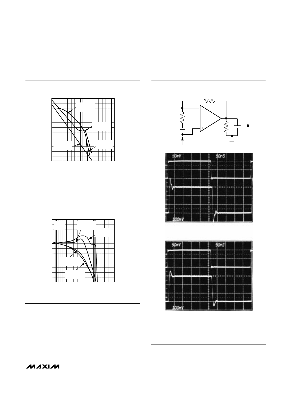
= 5pF) results in a peak in the gain of 3 amplifier configurations as shown in Figures 3 and 4.
Figure 3 shows a blow up of the open loop characteristics in the 10MHz to 200MHz frequency range, as well
as the corresponding closed loop characteristics for a
gain of three non-inverting amplifier at similar load conditions. It should be noted that the open loop characteristic does not show the additional phase shift covered
by the input capacitance pole. This is why the closed
loop peaking at 30 to 40MHz is greater than what
would be expected from the 50 to 60 degrees of phase
margin indicated by the open loop characteristics.
Corresponding small signal step response characteristics show well-behaved pulse waveforms with 16–33%
overshoot.
The input capacitive pole can be neutralized by adding
a feedback capacitor to R2. The value of capacitance
is selected according to R1CIN= R2CFB, where C
IN
is
the sum of the common mode and differential input
capacitance ≈5pF. For R2= 2R1, CFB= C
IN/2
≈ 2.5pF.
Figure 4 shows the results of this feedback capacitor
addition. Neutralizing the input capacitance demonstrates the peaking that can result from the loss of gain
margin at 70 to 100MHz. As the load time constant
(RLCL) increases the peaking gets progressively worse
≈6dB at RL= 2K, CL= 50pF. The step response wave-
forms are as expected with a very strong 88MHz ring
being exhibited at RL= 2k, CL= 50pF and no overshoot at RL= 50Ω, CL = 5pF.
Layout Considerations
As with any high-speed wideband amplifier, certain layout considerations are necessary to ensure stable operation. All connections to the amplifier should remain as
short as possible, and the power supplies bypassed with
0.1µF capacitors to signal ground. It is suggested that a
ground plane be considered as the best method for
ensuring stability because it minimizes stray inductance
and unwanted coupling in the ground signal paths.
To minimize capacitive effects, resistor values should be
kept as small as possible, consistent with the application.
MAX408 Offset Voltage Nulling
The configuration of Figure 2 will give a typical V
OS
nulling range of ±15mV. If a smaller adjustment range is
desired, resistor values R1 and R2 can be increased
accordingly. For example, at R1 = 3.6kΩ, the adjustment
range is ±5mV. Since pins 1 and 5 are not part of the signal path, AC characteristics are left undisturbed.
Single/Dual/Quad High-Speed, Fast-Settling,
High Output Current Operational Amplifier
8 _______________________________________________________________________________________
2
V+ BAL.
BAL.
5
6
1
3
R
2
= 1.3kΩR1 = 1.3k
RP = 10kΩ
Figure 2. VOSNulling Method for MAX408 Simplified Schematic. For MAX428/448 omit balance pins.
MAX408/428/448
Single/Dual/Quad High-Speed, Fast-Settling,
High Output Current Operational Amplifier
_______________________________________________________________________________________ 9
Figure 3. Frequency and Time Domain Response Characteristics, AV= 3
RL = 2Ω
C
L
= 50pF
R
L
= 50Ω
C
L
= 5pF
SMALL SIGNAL STEP RESPONSE
e
IN
e
O
e
IN
e
O
R
1 =
1kΩ
R2 = 2kΩ
e
o
/ eIN = (1 + R2 / R1) = 3V/V
R
L
e
IN
C
L
e
O
20
10
15
-10
10MHz 1GHz
OPEN LOOP FREQUENCY RESPONSE
5
0
-5
60
180
120
240
300
360
FREQUENCY
OPEN LOOP GAIN (A
V
, dB)
PHASE (φ, DEGREES)
100MHz
RL = 50Ω
C
L
= 5pF
A
V
,
RL = 2kΩ
C
L
= 50pF
φ,
RL = 2kΩ
C
L
= 50pF
A
V
,
RL = 50Ω
C
L
= 5pF
φ,
20
15
-10
1MHz 10MHz 100MHz 1GHz
CLOSED LOOP FREQUENCY RESPONSE
0
-5
315
270
225
180
135
90
45
0
10
5
FREQUENCY
CLOSED LOOP GAIN (A
V
, dB)
PHASE (φ, DEGREES)
RL = 50Ω
C
L
= 5pF
A
V
,
RL = 2kΩ
C
L
= 50pF
φ,
RL = 2kΩ
C
L
= 50pF
A
V
,
RL = 50Ω
C
L
= 5pF
φ,
R1 = 1k,
R
2
= 2k

MAX408/428/448
Single/Dual/Quad High-Speed, Fast-Settling,
High Output Current Operational Amplifier
10 ______________________________________________________________________________________
RL = 2kΩ
C
L
= 50pF
R
L
= 50Ω
C
L
= 5pF
SMALL SIGNAL STEP RESPONSE
e
IN
e
O
e
IN
e
O
C
IN
≈5pF
1kΩ
2kΩ
R
L
C
L
C
FB
= 2.5pF
e
O
e
IN
20
15
-10
1MHz 10MHz 100MHz 1GHz
CLOSED LOOP FREQUENCY RESPONSE
0
-5
315
270
225
180
135
90
45
0
10
5
FREQUENCY
CLOSED LOOP GAIN (A
V
, dB)
PHASE (φ, DEGREES)
RL = 50Ω
C
L
= 5pF
A
V
,
RL = 2kΩ
C
L
= 50pF
A
V
,
R1 = 1kΩ
R
2
= 2kΩ
Figure 4. Response Characteristics with Input Pole Cancellation, AV= 3

MAX408/428/448
Single/Dual/Quad High-Speed, Fast-Settling,
High Output Current Operational Amplifier
______________________________________________________________________________________ 11
PART
MAX428A_CPA
MAX428ACSA
MAX428CPA 0°C to +70°C
0°C to +70°C
0°C to +70°C
TEMP. RANGE PIN-PACKAGE
8 Lead Plastic DIP
8 Lead Small Outline
8 Lead Plastic DIP
MAX428CSA 0°C to +70°C 8 Lead Small Outline
MAX428C/D 0°C to +70°C Dice
MAX448ACPD
0°C to +70°C 14 Lead Plastic DIP
MAX448ACSD 0°C to +70°C
14 Lead Small
Outline
MAX448CPD 0°C to +70°C 14 Lead Plastic DIP
MAX448CSD 0°C to +70°C
14 Lead Small
Outline
MAX448C/D 0°C to +70°C Dice
Ordering Information (continued)

MAX408/428/448
Single/Dual/Quad High-Speed, Fast-Settling,
High Output Current Operational Amplifier
Maxim cannot assume responsibility for use of any circuitry other than circuitry entirely embodied in a Maxim product. No circuit patent licenses are
implied. Maxim reserves the right to change the circuitry and specifications without notice at any time.
12
____________________Maxim Integrated Products, 120 San Gabriel Drive, Sunnyvale, CA 94086 408-737-7600
© 1997 Maxim Integrated Products Printed USA is a registered trademark of Maxim Integrated Products.
NOTES
 Loading...