

General Description
The MAX4475–MAX4478/MAX4488/MAX4489 wideband, low-noise, low-distortion operational amplifiers
offer rail-to-rail outputs and single-supply operation
down to 2.7V. They draw 2.2mA of quiescent supply
current per amplifier while featuring ultra-low distortion
(0.0002% THD+N), as well as low input voltage-noise
density (4.5nV/√Hz) and low input current-noise density
(0.5fA/√Hz). These features make the devices an ideal
choice for applications that require low distortion and/or
low noise.
For power conservation, the MAX4475/MAX4488 offer a
low-power shutdown mode that reduces supply current
to 0.01µA and places the amplifiers’ outputs into a highimpedance state. These amplifiers have outputs which
swing rail-to-rail and their input common-mode voltage
range includes ground. The MAX4475–MAX4478 are
unity-gain stable with a gain-bandwidth product of
10MHz. The MAX4488/4489 are internally compensated
for gains of +5V/V or greater with a gain-bandwidth
product of 42MHz. The single MAX4475/MAX4476/
MAX4488 are available in space-saving, 6-pin SOT23
and TDFN packages.
Applications
ADC Buffers
DAC Output Amplifiers
Low-Noise Microphone/Preamplifiers
Digital Scales
Strain Gauges/Sensor Amplifiers
Medical Instrumentation
Features
o Low Input Voltage-Noise Density: 4.5nV/√Hz
o Low Input Current-Noise Density: 0.5fA/√Hz
o Low Distortion: 0.0002% THD+N (1kΩ load)
o Single-Supply Operation from +2.7V to +5.5V
o Input Common-Mode Voltage Range Includes
Ground
o Rail-to-Rail Output Swings with a 1kΩ Load
o 10MHz GBW Product, Unity-Gain Stable
(MAX4475–MAX4478)
o 42MHz GBW Product, Stable with AV≥ +5V/V
(MAX4488/MAX4489)
o Excellent DC Characteristics
VOS= 70µV
I
BIAS
= 1pA
Large-Signal Voltage Gain = 120dB
o Low-Power Shutdown Mode:
Reduces Supply Current to 0.01µA
Places Output in High-Impedance State
o Available in Space-Saving SOT23, TDFN, µMAX®,
and TSSOP Packages
MAX4475–MAX4478/MAX4488/MAX4489
SOT23, Low-Noise, Low-Distortion,
Wide-Band, Rail-to-Rail Op Amps
________________________________________________________________
Maxim Integrated Products
1
Ordering Information
Selector Guide
19-2137; Rev 5; 7/10
For pricing, delivery, and ordering information, please contact Maxim Direct at 1-888-629-4642,
or visit Maxim’s website at www.maxim-ic.com.
Ordering Information continued at end of data sheet.
+
Denotes a lead(Pb)-free/RoHS-compliant package.
*
EP = Exposed pad (connect to VSS).
/V denotes an automotive qualified part.
T = Tape and reel.
Pin Configurations and Typical Operating Circuit appear at
end of data sheet.
Typical Operating Characteristic
µMAX is a registered trademark of Maxim Integrated Products, Inc.
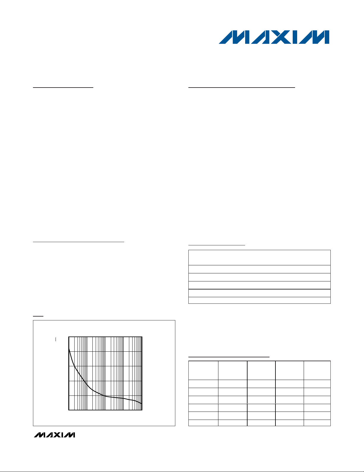
INPUT VOLTAGE-NOISE DENSITY
25
20
15
10
5
EQUIVALENT INPUT NOISE VOLTAGE (nV/√Hz)
IN
V
0
10 1k 10k100 100k
vs. FREQUENCY
MAX4475 toc20
FREQUENCY (Hz)
PART TEMP RANGE
MAX4475AUT+T
MAX4475AUA+ -40°C to +125°C 8 µMAX —
MAX4475ASA+ -40°C to +125°C 8 SO —
MAX4475ATT+T -40°C to +125°C 6 TDFN-EP* +ADD
MAX4475AUT/V+T -40°C to +125°C 6 SOT23 +ACQQ
-40°C to +125°C 6 SOT23 AAZV
PINPACKAGE
TOP
MARK
PART
MAX4475 10 1 1 Yes
MAX4476 10 1 1 —
MAX4477 10 1 2 —
MAX4478 10 1 4 —
MAX4488 42 5 1 Yes
MAX4489 42 5 2 —
G A IN B W
( M H z)
STABLE
GAIN
(V/V)
NO. OF
AMPS
SHDN
MAX4475–MAX4478/MAX4488/MAX4489
SOT23, Low-Noise, Low-Distortion,
Wide-Band, Rail-to-Rail Op Amps
2 _______________________________________________________________________________________
ABSOLUTE MAXIMUM RATINGS
DC ELECTRICAL CHARACTERISTICS
(VDD= +5V, VSS= 0V, VCM= 0V, V
OUT
= VDD/2, RLtied to VDD/2, SHDN = VDD, TA= -40°C to +125°C, unless otherwise noted.
Typical values are at T
A
= +25°C.) (Notes 1, 2)
Stresses beyond those listed under “Absolute Maximum Ratings” may cause permanent damage to the device. These are stress ratings only, and functional
operation of the device at these or any other conditions beyond those indicated in the operational sections of the specifications is not implied. Exposure to
absolute maximum rating conditions for extended periods may affect device reliability.
Power-Supply Voltage (VDDto VSS) ......................-0.3V to +6.0V
Analog Input Voltage (IN_+, IN_-)....(V
SS
- 0.3V) to (VDD+ 0.3V)
SHDN Input Voltage....................................(V
SS
- 0.3V) to +6.0V
Output Short-Circuit Duration to Either Supply ..........Continuous
Continuous Input Current (IN+, IN-) .................................±10mA
Continuous Power Dissipation (T
A
= +70°C)
6-Pin SOT23 (derate 9.1mW/°C above +70°C)...........727mW
6-Pin TDFN (derate 18.2mW/°C above 70°C)...........1454mW
8-Pin µMAX (derate 4.5mW/°C above +70°C) ............362mW
8-Pin SO (derate 5.88mW/°C above +70°C)...............471mW
14-Pin SO (derate 8.33mW/°C above +70°C)..............667mW
14-Pin TSSOP (derate 9.1mW/°C above +70°C) .........727mW
Operating Temperature Range .........................-40°C to +125°C
Junction Temperature......................................................+150°C
Storage Temperature Range .............................-65°C to +150°C
Lead Temperature (soldering, 10s) .................................+300°C
Soldering Temperature (reflow)
SOT23, µMAX, TSSOP, TDFN, and 8-Pin SO...............+260°C
14-Pin SO.....................................................................+240°C
Supply Voltage Range V
Quiescent Supply Current Per
Amplifier
Input Offset Voltage V
Input Offset Voltage Tempco TC
Input Bias Current I
Input Offset Current I
Differential Input Resistance R
Input Common-Mode Voltage
Range
Common-Mode Rejection Ratio CMRR
Power-Supply Rejection Ratio PSRR VDD = 2.7 to 5.5V 90 120 dB
Large-Signal Voltage Gain A
PARAMETER SYMBOL CONDITIONS MIN TYP MAX UNITS
(Note 3) 2.7 5.5 V
DD
Normal mode
I
D
Shutdown mode (SHDN = VSS) (Note 2) 0.01 1.0 µA
TA = +25°C ±70 ±350
OS
TA = -40°C to +125°C ±750
VOS
(Note 4) ±1 ±150 pA
B
(Note 4) ±1 ±150 pA
OS
IN
V
Guaranteed by
CM
CMRR Test
(VSS - 0.2V) ≤
V
CM
1.6V)
(V
SS
V
CM
1.7V)
RL = 10kΩ to VDD/2;
V
OUT
RL = 1kΩ to VDD/2;
VOL
V
OUT
RL = 500Ω to VDD/2;
V
OUT
≤ (VDD -
- 0.1V) ≤
≤ (VDD -
= 100mV to (V
= 200mV to (V
= 350mV to (V
VDD = 3V 2.2
V
= 5V 2.5 4.4
DD
±0.3 ±6 µV/°C
1000 GΩ
TA = +25°C-0.2V
= -40°C to +125°C-0.1 V
T
A
TA = +25°C 90 115
TA = -40°C to +125°C90
DD
DD
DD
- 125mV)
- 250mV)
- 500mV)
90 120
85 110
85 110
D D
D D
- 1.6
- 1.7
mA
µV
V
dB
dB
MAX4475–MAX4478/MAX4488/MAX4489
SOT23, Low-Noise, Low-Distortion,
Wide-Band, Rail-to-Rail Op Amps
_______________________________________________________________________________________ 3
DC ELECTRICAL CHARACTERISTICS (continued)
(VDD= +5V, VSS= 0V, VCM= 0V, V
OUT
= VDD/2, RLtied to VDD/2, SHDN = VDD, TA= -40°C to +125°C, unless otherwise noted.
Typical values are at T
A
= +25°C.) (Notes 1, 2)
AC ELECTRICAL CHARACTERISTICS
(VDD= +5V, VSS= 0V, VCM= 0V, V
OUT
= VDD/2, RLtied to VDD/2, SHDN = VDD, TA= +25°C.)
PARAMETER SYMBOL CONDITIONS MIN TYP MAX UNITS
Output Voltage Swing V
Output Short-Circuit Current I
Output Leakage Current I
SHDN Logic Low V
SHDN Logic High V
SHDN Input Current SHDN = VSS to V
Input Capacitance C
OUT
SC
LEAK
IL
IH
IN
|V
IN+
R
L
|V
IN+
R
L
|V
IN+
R
L
Shutdown mode (SHDN = VSS),
V
OUT
| ≥ 10mV,
- V
IN-
= 10kΩ to V
| ≥ 10mV,
- V
IN-
= 1kΩ to V
| ≥ 10mV,
- V
IN-
= 500Ω to V
= VSS to V
DD
DD
DD
/2
/2
/2
DD
DD
PARAMETER SYMBOL CONDITIONS MIN TYP MAX UNITS
Gain-Bandwidth Product GBWP
Slew Rate SR
Full-Power Bandwidth (Note 5)
MAX4475–MAX4478 AV = +1V/V 10
MAX4488/MAX4489 A
MAX4475–MAX4478 AV = +1V/V 3
MAX4488/MAX4489 A
MAX4475–MAX4478 AV = +1V/V 0.4
MAX4488/MAX4489 A
V
- V
DD
OH
V
- V
OL
SS
V
- V
DD
OH
V
- V
OL
SS
V
- V
DD
OH
V
- V
OL
SS
0.7 x V
DD
= +5V/V 42
V
= +5V/V 10
V
= +5V/V 1.25
V
10 45
10 40
80 200
50 150
mV
100 300
80 250
48 mA
±0.001 ±1.0 µA
0.3 x V
D D
V
V
0.01 1 µA
10 pF
MHz
V/µs
MHz
Peak-to-Peak Input Noise Voltage
e
Input Voltage-Noise Density e
Input Current-Noise Density i
Total Harmonic Distortion Plus
Noise (Note 6)
THD + N
n
f = 0.1Hz to 10Hz 260 nV
-
P-P
f = 10Hz 21
f = 1kHz 4.5
n
nV/√Hz
f = 30kHz 3.5
f = 1kHz 0.5 fA/√Hz
n
V
OUT
A
= +1V/V
V
(MAX4475–MAX4478),
= 10kΩ to GND
R
L
V
OUT
= +1V/V
A
V
(MAX4475–MAX4478),
= 1kΩ to GND
R
L
V
OUT
A
= +5V/V
V
(MAX4488/MAX4489),
= 10kΩ to GND
R
L
= 2V
= 2V
= 2V
P-P
P-P
P-P
,
f = 1kHz 0.0002
f = 20kHz 0.0007
,
,
f = 1kHz 0.0002
f = 20kHz 0.001
f = 1kHz 0.0004
%
f = 20kHz 0.0006
4
2
10
8
6
12
14
16
18
-50 -30 -20-40 -100 1020304050
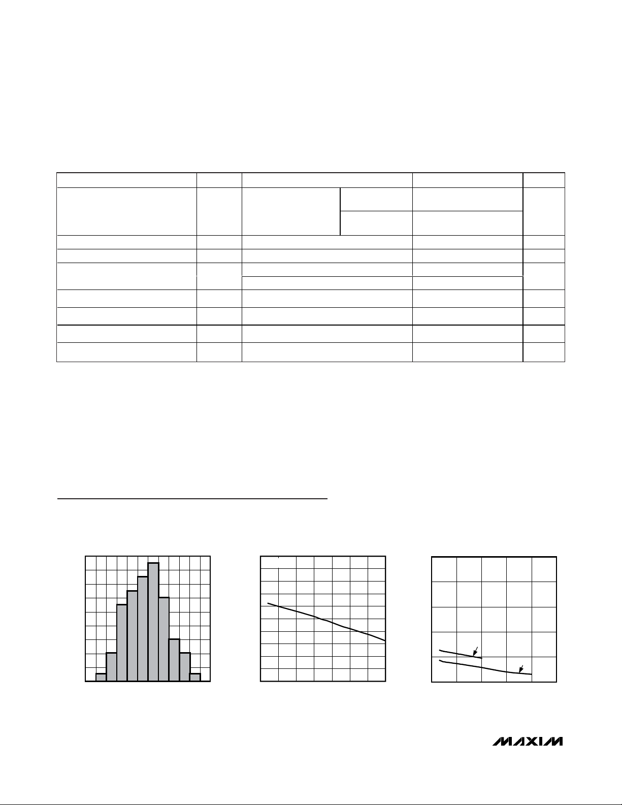
INPUT OFFSET VOLTAGE DISTRIBUTION
MAX4475-8 toc1
VOS (µV)
PERCENTAGE OF UNITS (%)
0
-250
-100
-150
-200
0
-50
200
150
100
50
250
-50 -25 0 25 50 75 100 125
OFFSET VOLTAGE vs. TEMPERATURE
MAX4475 toc02
TEMPERATURE (°C)
INPUT OFFSET VOLTAGE (µV)
V
COM
= 0V
0
10
30
20
40
50
-0.5 1.50.5 2.5 3.5 4.5
INPUT OFFSET VOLTAGE
vs. INPUT COMMON-MODE VOLTAGE
MAX4475 toc03
INPUT COMMON-MODE VOLTAGE (V)
INPUT OFFSET VOLTAGE (µV)
VDD = 3V
V
DD
= 5V
Typical Operating Characteristics
(VDD= +5V, VSS= 0V, VCM= 0V, V
OUT
= VDD/2, RLtied to VDD/2, input noise floor of test equipment =10nV/√Hz for all distortion
measurements, T
A
= +25°C, unless otherwise noted.)
MAX4475–MAX4478/MAX4488/MAX4489
SOT23, Low-Noise, Low-Distortion,
Wide-Band, Rail-to-Rail Op Amps
4 _______________________________________________________________________________________
Note 1: All devices are 100% tested at TA= +25°C. Limits over temperature are guaranteed by design.
Note 2: SHDN is available on the MAX4475/MAX4488 only.
Note 3: Guaranteed by the PSRR test.
Note 4: Guaranteed by design.
Note 5: Full-power bandwidth for unity-gain stable devices (MAX4475–MAX4478) is measured in a closed-loop gain of +2V/V to
accommodate the input voltage range, V
OUT
= 4V
P-P
.
Note 6: Lowpass-filter bandwidth is 22kHz for f = 1kHz and 80kHz for f = 20kHz. Noise floor of test equipment = 10nV/√Hz.
AC ELECTRICAL CHARACTERISTICS (continued)
(VDD= +5V, VSS= 0V, VCM= 0V, V
OUT
= VDD/2, RLtied to VDD/2, SHDN = VDD, TA= +25°C.)
PARAMETER SYMBOL CONDITIONS MIN TYP MAX UNITS
Total Harmonic Distortion Plus
Noise (Note 6)
Capacitive-Load Stability No sustained oscillations 200 pF
Gain Margin GM 12 dB
Phase Margin ΦM
Settling Time To 0.01%, V
Delay Time to Shutdown t
Enable Delay Time from Shutdown t
,
= 2V
V
OUT
THD + N
P-P
= +5V/V
A
V
(MAX4488/MAX4489),
R
= 1kΩ to GND
L
f = 1kHz 0.0005
f = 20kHz 0.008
MAX4475–MAX4478, AV = +1V/V 70
MAX4488/MAX4489, A
SH
V
EN
OUT
OUT
= 2.5V, V
OUT
= +5V/V 80
V
= 2V step 2 µs
settles to 0.1% 10 µs
1.5 µs
%
degrees
Power-Up Delay Time VDD = 0 to 5V step, V
stable to 0.1% 13 µs
OUT
Typical Operating Characteristics (continued)
(VDD= +5V, VSS= 0V, VCM= 0V, V
OUT
= VDD/2, RLtied to VDD/2, input noise floor of test equipment =10nV/√Hz for all distortion
measurements, T
A
= +25°C, unless otherwise noted.)
MAX4475–MAX4478/MAX4488/MAX4489
SOT23, Low-Noise, Low-Distortion,
Wide-Band, Rail-to-Rail Op Amps
_______________________________________________________________________________________
5
OUTPUT VOLTAGE
vs. OUTPUT LOAD CURRENT
0.25
VDD = 3V OR 5V
= ±10mV
V
DIFF
0.20
0.15
VDD - V
0.10
OUTPUT VOLTAGE (V)
0.05
0
045231678910
OUTPUT LOAD CURRENT (mA)
OH
V
OL
LARGE-SIGNAL VOLTAGE GAIN
vs. OUTPUT VOLTAGE SWING
130
120
110
100
(dB)
V
A
90
80
70
60
50
RL = 2k
0 50 100 150 200 250
V
SWING FROM EITHER SUPPLY (mV)
OUT
Ω
RL = 20k
R
RL = 200k
Ω
REFERENCED TO GND
L
LARGE-SIGNAL VOLTAGE GAIN
vs. OUTPUT VOLTAGE SWING
130
RL = 200k
120
110
100
(dB)
90
V
A
80
70
60
50
0 50 100 150 200 250
Ω
RL = 20k
Ω
V
SWING FROM EITHER SUPPLY (mV)
OUT
RL = 2k
REFERENCED TO V
R
L
Ω
OUTPUT VOLTAGE SWING (VOL)
vs. TEMPERATURE
70
60
50
40
30
20
10
0
-50 0 25-25 50 75 100 125
RL = 1k
TEMPERATURE (°C)
LARGE-SIGNAL VOLTAGE GAIN
vs. OUTPUT VOLTAGE SWING
130
120
RL = 2k
110
100
90
80
70
60
50
0 50 100 150 200 250
V
SWING FROM EITHER SUPPLY (mV)
OUT
Ω
R
SUPPLY CURRENT vs. TEMPERATURE
3.0
PER AMPLIFIER
2.5
2.0
1.5
1.0
0.5
0
-50 25 50-25 0 75 100 125
TEMPERATURE (°C)
Ω
VDD = 3V
VDD = 5V
DD
MAX4475 toc04
MAX4475 toc07
MAX4475 toc10
OUTPUT VOLTAGE SWING (VOH)
vs. TEMPERATURE
70
60
50
(mV)
40
OH
- V
30
DD
V
20
10
0
-50 0 25-25 50 75 100 125
RL = 1k
Ω
RL = 10k
TEMPERATURE (°C)
LARGE-SIGNAL VOLTAGE GAIN
vs. OUTPUT VOLTAGE SWING
130
120
110
100
(dB)
90
V
A
80
70
60
50
0 50 100 150 200 250
V
SWING FROM EITHER SUPPLY (mV)
OUT
RL = 2k
RL = 20k
Ω
Ω
REFERENCED TO V
R
L
LARGE-SIGNAL VOLTAGE GAIN
vs. TEMPERATURE
140
130
120
110
100
(dB)
VOL
90
A
80
70
60
V
OUT
50
-50 0 25-25 50 75 100 125
RL = 10k
= 150mV TO 4.75V
TEMPERATURE (°C)
RL = 100k
Ω
Ω
RL = 200k
VDD = 3V
Ω
MAX4475 toc05
(mV)
OL
V
MAX4475 toc08
Ω
(dB)
V
A
DD
MAX4475 toc11
SUPPLY CURRENT (mA)
Ω
RL = 10k
RL = 200k
RL = 20k
Ω
REFERENCED TO GND
L
VDD = 5V
MAX4475 toc06
Ω
MAX4475 toc09
Ω
MAX4475 toc12
MAX4475–MAX4478/MAX4488/MAX4489
SOT23, Low-Noise, Low-Distortion,
Wide-Band, Rail-to-Rail Op Amps
6 _______________________________________________________________________________________
Typical Operating Characteristics (continued)
(VDD= +5V, VSS= 0V, VCM= 0V, V
OUT
= VDD/2, RLtied to VDD/2, input noise floor of test equipment =10nV/√Hz for all distortion
measurements, T
A
= +25°C, unless otherwise noted.)
0
1.0
0.5
2.0
1.5
2.5
3.0
2.5 3.5 4.03.0 4.5 5.0 5.5
SUPPLY CURRENT vs. SUPPLY VOLTAGE
MAX4475 toc13
SUPPLY VOLTAGE (V)
SUPPLY CURRENT (mA)
PER AMPLIFIER
0
1.0
0.5
2.0
1.5
2.5
3.0
021345
SUPPLY CURRENT vs. OUTPUT VOLTAGE
MAX4475 toc14
OUTPUT VOLTAGE (V)
SUPPLY CURRENT (mA)
VDD = 5V
V
DD
= 3V
-20
-15
-10
-5
0
5
10
15
20
2.5 3.53.0 4.0 4.5 5.0 5.5
INPUT OFFSET VOLTAGE
vs. SUPPLY VOLTAGE
MAX4475 toc15
SUPPLY VOLTAGE (V)
INPUT OFFSET VOLTAGE (µV)
MAX4475–MAX4478
GAIN AND PHASE vs. FREQUENCY
INPUT FREQUENCY (Hz)
100 100k 1M 10M1k 10k 100M
GAIN (dB)
60
-40
-30
-20
-10
0
10
20
50
40
30
-180
PHASE (degrees)
180
-144
-108
-72
-36
0
36
144
108
72
MAX4475 toc16
VDD = 3V OR 5V
R
L
= 50k
Ω
C
L
= 20pF
A
V
= +1000V/V
GAIN
PHASE
MAX4488/MAX4489
GAIN AND PHASE vs. FREQUENCY
INPUT FREQUENCY (Hz)
100 100k 1M 10M1k 10k 100M
GAIN (dB)
60
-40
-30
-20
-10
0
10
20
50
40
30
-180
PHASE (degrees)
180
-144
-108
-72
-36
0
36
144
108
72
MAX4475 toc17
VDD = 3V OR 5V
R
L
= 50k
Ω
C
L
= 20pF
A
V
= +1000V/V
GAIN
PHASE
1000 100,000
-130
-10
-20
-30
-40
-50
-60
-70
-80
-90
-100
-110
-120
0
0.001 0.1 10
MAX4475–MAX4478
POWER-SUPPLY REJECTION RATIO
vs. FREQUENCY
MAX4475 toc18
FREQUENCY (kHz)
PSRR (dB)
VDD = 3V OR 5V
1000
100
10
1
0.1
0.01
1 100 1k10 10k
OUTPUT IMPEDANCE vs. FREQUENCY
MAX4475 toc19
FREQUENCY (Hz)
OUTPUT IMPEDANCE (Ω)
AV = +5
AV = +1
MAX4475–MAX4478/MAX4488/MAX4489
SOT23, Low-Noise, Low-Distortion,
Wide-Band, Rail-to-Rail Op Amps
_______________________________________________________________________________________
7
Typical Operating Characteristics (continued)
(VDD= +5V, VSS= 0V, VCM= 0V, V
OUT
= VDD/2, RLtied to VDD/2, input noise floor of test equipment =10nV/√Hz for all distortion
measurements, T
A
= +25°C, unless otherwise noted.)
1µs/div
MAX4475–MAX4478
LARGE-SIGNAL PULSE RESPONSE
VDD = 3V, RL = 10kΩ, CL = 100pF
V
IN
= 2V
0.5V
MAX4475 toc27
2.5V
4µs/div
MAX4475–MAX4478
SMALL-SIGNAL PULSE RESPONSE
VDD = 3V, RL = 10kΩ, CL = 100pF
V
IN
= 100mV PULSE
0.5V
MAX4475 toc28
0.6V
20mV/div
INPUT VOLTAGE-NOISE DENSITY
vs. FREQUENCY
25
20
15
10
5
EQUIVALENT INPUT NOISE VOLTAGE (nV/√Hz)
IN
V
0
10 1k 10k100 100k
FREQUENCY (Hz)
MAX4488/MAX4489
TOTAL HARMONIC DISTORTION PLUS NOISE
vs. OUTPUT VOLTAGE SWING
10
AV = +5
= 100k
R
Ω
L
1
0.1
MAX4475
vs. OUTPUT VOLTAGE SWING
Ω
fO = 20kHz, FILTER BW = 80kHz
OUTPUT VOLTAGE (V
MAX4475–MAX4478
vs. FREQUENCY
= 2V
P-P
Ω
MAX4475 toc20
MAX4475 toc23
200nV/div
0.01
0.1Hz TO 10Hz
VDD = 3V OR 5V
NOISE = 260nV
V
P-P
P-P
1s/div
P-P
NOISE
MAX4488/MAX4489
TOTAL HARMONIC DISTORTION
PLUS NOISE vs. FREQUENCY
MAX4475 toc21
MAX4475 toc24
TOTAL HARMONIC DISTORTION PLUS NOISE
10
AV = +1
= 100k
R
L
1
0.1
THD + N (%)
0.01
0.001
fO = 3kHz, FILTER BW = 30kHz
0.0001
02134
TOTAL HARMONIC DISTORTION PLUS NOISE
0.01
FILTER BW = 80kHz
V
OUT
AV = +1
= 1k
R
L
MAX4475 toc22
)
P-P
MAX4475 toc25
0.01
THD + N (%)
0.001
0.0001
0.00001
VDD = 3V, fO = 3kHz
FILTER BW = 30kHz
0213
OUTPUT VOLTAGE (V
MAX4488/MAX4489
TOTAL HARMONIC DISTORTION PLUS NOISE
1
FILTER BW = 80kHz
R
R
V
0.1
0.01
THD + N (%)
0.001
0.0001
0 5k 15k 20k
vs. FREQUENCY
= 10kΩ TO GND
L
= 2.43kΩ, R2 = 10k
1
= 2.75V
OUT
P-P
FREQUENCY (Hz)
VDD = +3V, fO = 20kHz
FILTER BW = 80kHz
P-P
Ω
AV = +5, VDD = 3V
AV = +5, VDD = 5V
10k
0.001
THD + N (%)
FILTER BW = 22kHz
= 10kΩ TO GND
R
L
R1 = 5.6kΩ, R2 = 53k
= 2V
V
OUT
0.0001
0 10k 20k
)
MAX4475 toc26
P-P
5k 15k
AV = +10, VDD = 3V
AV = +10, VDD = 5V
Ω
FREQUENCY (Hz)
THD + N (%)
RL TO VDD/2
0.001
0 20k
5k 10k 15k
FREQUENCY (Hz)
RL TO GND
RL TO V
DD

Pin Description
MAX4475–MAX4478/MAX4488/MAX4489
SOT23, Low-Noise, Low-Distortion,
Wide-Band, Rail-to-Rail Op Amps
8 _______________________________________________________________________________________
Typical Operating Characteristics (continued)
(VDD= +5V, VSS= 0V, VCM= 0V, V
OUT
= VDD/2, RLtied to VDD/2, input noise floor of test equipment =10nV/√Hz for all distortion
measurements, T
A
= +25°C, unless otherwise noted.)
1µs/div
MAX4488/MAX4489
LARGE-SIGNAL PULSE RESPONSE
VDD = 3V, RL = 10kΩ, CL = 50pF
V
IN
= 20mV PULSE, AV = +5V/V
MAX4475 toc29
V
OUT
200mV/div
1µs/div
MAX4488/MAX4489
SMALL-SIGNAL PULSE RESPONSE
VDD = 3V, RL = 10kΩ, CL = 50pF
V
IN
= 20mV PULSE, AV = +5V/V
MAX4475 toc30
V
OUT
50mV/div
1.6V
1.5V
-20
-90
10 1000100 100k 100M10M
MAX4477/MAX4478/MAX4489
CROSSTALK vs. FREQUENCY
-60
-50
-40
-30
MAX4475 toc31
FREQUENCY (Hz)
CROSSTALK (dB)
10k 1M
-70
-80
PIN
MAX4475/
MAX4488
MAX4475/
MAX4488
MAX4476
MAX4477/
MAX4489
MAX4478
SOT23/TDFN SO/µMAX SOT23/TDFN SO/µMAX SO/TSSOP
OUT, OUTA,
1 6 1 1, 7 1, 7, 8, 14
OUTB, OUTC,
242411
IN+, INA+,
3 3 3 3, 5 3, 5, 10, 12
4 2 4 2, 6 2, 6, 9, 13
67684
58———
— 1, 5 5 — — N.C.
EP (TDFN
only)
—
EP (TDFN
only)
—— EP
INB+, INC+,
IN-, INA-, INB-,
INC-, IND-
NAME FUNCTION
OUTD
V
SS
IND+
V
DD
SHDN
Amplifier Output
Negative Supply. Connect
to ground for singlesupply operation
Noninverting Amplifier
Input
Inverting Amplifier Input
Positive Supply
Shutdown Input. Connect
to V
for normal
DD
operation (amplifier(s)
enabled).
No Connection. Not
internally connected.
Exposed Paddle. Connect
to V
.
SS

Detailed Description
The MAX4475–MAX4478/MAX4488/MAX4489 singlesupply operational amplifiers feature ultra-low noise
and distortion. Their low distortion and low noise make
them ideal for use as preamplifiers in wide dynamicrange applications, such as 16-bit analog-to-digital
converters (see
Typical Operating Circuit
). Their highinput impedance and low noise are also useful for signal conditioning of high-impedance sources, such as
piezoelectric transducers.
These devices have true rail-to-rail ouput operation,
drive loads as low as 1kΩ while maintining DC accuracy, and can drive capactive loads up to 200pF without
oscillation. The input common-mode voltage range
extends from (VDD- 1.6V) to 200mV below the negative
rail. The push-pull output stage maintains excellent DC
characteristics, while delivering up to ±5mA of current.
The MAX4475–MAX4478 are unity-gain stable, while
the MAX4488/MAX4489 have a higher slew rate and
are stable for gains ≥ 5V/V. The MAX4475/MAX4488
feature a low-power shutdown mode, which reduces
the supply current to 0.01µA and disables the outputs.
Low Distortion
Many factors can affect the noise and distortion that the
device contributes to the input signal. The following
guidelines offer valuable information on the impact of
design choices on Total Harmonic Distortion (THD).
Choosing proper feedback and gain resistor values for
a particular application can be a very important factor
in reducing THD. In general, the smaller the closedloop gain, the smaller the THD generated, especially
when driving heavy resistive loads. The THD of the part
normally increases at approximately 20dB per decade,
as a function of frequency. Operating the device near
or above the full-power bandwidth significantly
degrades distortion.
Referencing the load to either supply also improves the
part’s distortion performance, because only one of the
MOSFETs of the push-pull output stage drives the output. Referencing the load to midsupply increases the
part’s distortion for a given load and feedback setting.
(See the Total Harmonic Distortion vs. Frequency graph
in the
Typical Operating Characteristics
.)
For gains ≥ 5V/V, the decompensated devices
MAX4488/MAX4489 deliver the best distortion performance, since they have a higher slew rate and provide
a higher amount of loop gain for a given closed-loop
gain setting. Capacitive loads below 100pF do not significantly affect distortion results. Distortion performance is relatively constant over supply voltages.
MAX4475–MAX4478/MAX4488/MAX4489
SOT23, Low-Noise, Low-Distortion,
Wide-Band, Rail-to-Rail Op Amps
_______________________________________________________________________________________ 9
Figure 1. Adding Feed-Forward Compensation
Figure 2a. Pulse Response with No Feed-Forward
Compensation
Figure 2b. Pulse Response with 10pF Feed-Forward
Compensation
C
Z
R
F
R
G
V
IN
AV = +2
= RG = 100kΩ
R
F
V
100mV
0V
2µs/div
AV = +2
= RG = 100kΩ
R
F
2µs/div
IN
100mV/div
V
OUT
100mV/div
V
IN
100mV/div
V
OUT
100mV/div
V
OUT
MAX4475–MAX4478/MAX4488/MAX4489
SOT23, Low-Noise, Low-Distortion,
Wide-Band, Rail-to-Rail Op Amps
10 ______________________________________________________________________________________
Low Noise
The amplifier’s input-referred noise-voltage density is
dominated by flicker noise at lower frequencies, and by
thermal noise at higher frequencies. Because the thermal noise contribution is affected by the parallel combination of the feedback resistive network (R
F
|| RG,
Figure 1), these resistors should be reduced in cases
where the system bandwidth is large and thermal noise
is dominant. This noise contribution factor decreases,
however, with increasing gain settings.
For example, the input noise-voltage density of the circuit with R
F
= 100kΩ, RG= 11kΩ (AV= +5V/V) is
en= 14nV/√Hz, encan be reduced to 6nV/√Hz by
choosing RF= 10kΩ, RG= 1.1kΩ (AV= +5V/V), at the
expense of greater current consumption and potentially
higher distortion. For a gain of 100V/V with R
F
= 100kΩ,
RG= 1.1kΩ, the enis still a low 6nV/√Hz.
Using a Feed-Forward Compensation
Capacitor, C
Z
The amplifier’s input capacitance is 10pF. If the resistance seen by the inverting input is large (feedback
network), this can introduce a pole within the amplifier’s
bandwidth resulting in reduced phase margin.
Compensate the reduced phase margin by introducing
a feed-forward capacitor (CZ) between the inverting
input and the output (Figure 1). This effectively cancels
the pole from the inverting input of the amplifier.
Choose the value of C
Z
as follows:
C
Z
= 10 x (RF/ RG) [pF]
In the unity-gain stable MAX4475–MAX4478, the use of
a proper CZis most important for AV= +2V/V, and
AV = -1V/V. In the decompensated MAX4488/
MAX4489, CZis most important for AV= +10V/V.
Figures 2a and 2b show transient response both with
and without CZ.
Using a slightly smaller CZthan suggested by the formula above achieves a higher bandwidth at the
expense of reduced phase and gain margin. As a general guideline, consider using CZfor cases where RG||
RFis greater than 20kΩ (MAX4475–MAX4478) or
greater than 5kΩ (MAX4488/MAX4489).
Applications Information
The MAX4475–MAX4478/MAX4488/MAX4489 combine
good driving capability with ground-sensing input and
rail-to-rail output operation. With their low distortion and
low noise, they are ideal for use in ADC buffers, medical instrumentation systems and other noise-sensitive
applications.
Ground-Sensing and Rail-to-Rail Outputs
The common-mode input range of these devices
extends below ground, and offers excellent commonmode rejection. These devices are guaranteed not to
undergo phase reversal when the input is overdriven
(Figure 3).
Figure 4 showcases the true rail-to-rail output operation
of the amplifier, configured with AV= 5V/V. The output
swings to within 8mV of the supplies with a 10kΩ load,
making the devices ideal in low-supply voltage applications.
Power Supplies and Layout
The MAX4475–MAX4478/MAX4488/MAX4489 operate
from a single +2.7V to +5.5V power supply or from dual
supplies of ±1.35V to ±2.75V. For single-supply operation, bypass the power supply with a 0.1µF ceramic
Figure 3. Overdriven Input Showing No Phase Reversal
Figure 4. Rail-to-Rail Output Operation
AV = +1
= +5V
V
DD
= 10kΩ
R
L
0V
40µs/div
5V
0V
20µs/div
V
IN
2V/div
V
OUT
2V/div
V
OUT
1V/div

MAX4475–MAX4478/MAX4488/MAX4489
______________________________________________________________________________________ 11
capacitor placed close to the VDDpin. If operating from
dual supplies, bypass each supply to ground.
Good layout improves performance by decreasing the
amount of stray capacitance and noise at the op amp’s
inputs and output. To decrease stray capacitance, minimize PC board trace lengths and resistor leads, and
place external components close to the op amp’s pins.
Typical Application Circuit
The
Typical Application Circuit
shows the single
MAX4475 configured as an output buffer for the
MAX5541 16-bit DAC. Because the MAX5541 has an
unbuffered voltage output, the input bias current of the
op amp used must be less than 6nA to maintain 16-bit
accuracy. The MAX4475 has an input bias current of
only 150pA (max), virtually eliminating this as a source
of error. In addition, the MAX4475 has excellent openloop gain and common-mode rejection, making this an
excellent ouput buffer amplifier.
DC-Accurate Lowpass Filter
The MAX4475–MAX4478/MAX4488/MAX4489 offer a
unique combination of low noise, wide bandwidth, and
high gain, making them an excellent choice for active
filters up to 1MHz. The
Typical Operating Circuit
shows
the dual MAX4477 configured as a 5th order
Chebyschev filter with a cutoff frequency of 100kHz.
The circuit is implemented in the Sallen-Key topology,
making this a DC-accurate filter.
SOT23, Low-Noise, Low-Distortion,
Wide-Band, Rail-to-Rail Op Amps
Typical Application Circuit
Typical Operating Circuit
SERIAL
INTERFACE
3.09kΩ
1%
CS
SCLK
DIN
7.87kΩ
1%
220pF
10.0kΩ
470pF
1%
+5V
V
DD
U1
MAX5541ESA
DGND
3
1/2
2
5V
8
MAX4477
4
10.0kΩ
REF
AGND
0.1µF
1%
OUT
+2.5V
+5V
7
3
2
8
4
SHDN
MAX
U2
4475AUA
6
0 to +2.5V
OUTPUT
220pF
3.83kΩ
1
1%
13.7kΩ
1%
220pF
10.0kΩ
1%
5
MAX4477
1/2
6
15.0kΩ
1%
7.15kΩ
7
1%
220pF
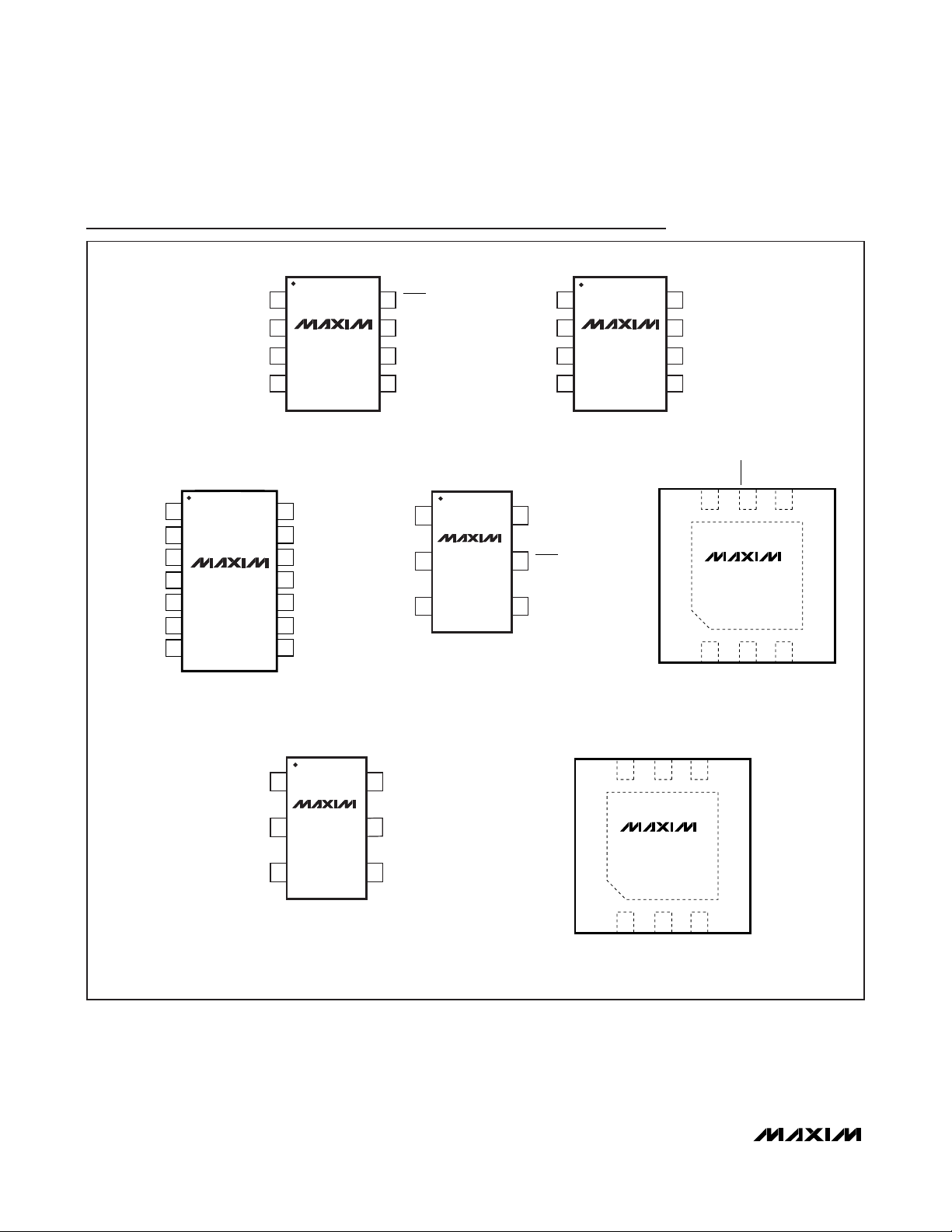
Pin Configurations
MAX4475–MAX4478/MAX4488/MAX4489
12 ______________________________________________________________________________________
SOT23, Low-Noise, Low-Distortion,
Wide-Band, Rail-to-Rail Op Amps
TOP VIEW
OUTA
INA-
INA+
V
INB+
INB-
TOP VIEW
N.C.
INA-
1
2
SHDN
8
V
7
DD
MAX4475
INA+
MAX4488
3
4
SS
OUT
6
N.C.V
5
SO/µMAX
TOP VIEW
1
2
3
4
DD
MAX4478
5
6
7
14
OUTD
13
IND-
12
IND+
11
V
SS
10
INC+
9
INC-
OUTCOUTB
8
16V
OUT
V
SS
MAX4475
2
MAX4488
34
SOT23-6
SO/TSSOP
TOP VIEW
OUTA
INA-
INA+
5
SHDN
IN-IN+
1
2
V
8
DD
OUTB
7
MAX4477
MAX4489
3
4
SS
INB-
6
INB+V
5
SO/µMAX
DD
V
TOP VIEW
DD
SHDN4IN-
6
5
MAX4475
MAX4488
*EP
+
123
SS
IN+
V
OUT
*EP = EXPOSED PADDLE.
TDFN
TOP VIEW
OUT
V
SS
16V
MAX4476
2
5
TOP VIEW
DD
N.C.
DD
V
N.C.4IN-
6
5
MAX4476
34
SOT23-6
IN-IN+
*EP
+
123
SS
V
OUT
*EP = EXPOSED PADDLE.
TDFN
IN+
MAX4475–MAX4478/MAX4488/MAX4489
Ordering Information (continued)
SOT23, Low-Noise, Low-Distortion,
Wide-Band, Rail-to-Rail Op Amps
______________________________________________________________________________________ 13
Chip Information
PROCESS: BiCMOS
+
Denotes a lead(Pb)-free/RoHS-compliant package.
*
EP = Exposed pad (connect to VSS).
/V denotes an automotive qualified part.
T = Tape and reel.
PART TEMP RANGE
MAX4476AUT+T
MAX4476ATT+T -40°C to +125°C 6 TDFN-EP* +ADF
MAX4477AUA+
MAX4477AUA+ -40°C to +125°C 8 µMAX —
MAX4477ASA+ -40°C to +125°C 8 SO —
MAX4478AUD+
MAX4478AUD/V+ -40°C to +125°C 14 TSSOP —
MAX4478ASD+ -40°C to +125°C 14 SO —
MAX4488AUT+T
MAX4488AUA+ -40°C to +125°C 8 µMAX —
MAX4488ASA+ -40°C to +125°C 8 SO —
MAX4488ATT+T -40°C to +125°C 6 TDFN-EP* +ADE
MAX4489AUA+
-40°C to +125°C 6 SOT23 AAZX
-40°C to +125°C 8 µMAX —
-40°C to +125°C 14 TSSOP —
-40°C to +125°C 6 SOT23 AAZW
-40°C to +125°C 8 µMAX —
PINPACKAGE
TOP
MARK
MAX4475–MAX4478/MAX4488/MAX4489
SOT23, Low-Noise, Low-Distortion,
Wide-Band, Rail-to-Rail Op Amps
14 ______________________________________________________________________________________
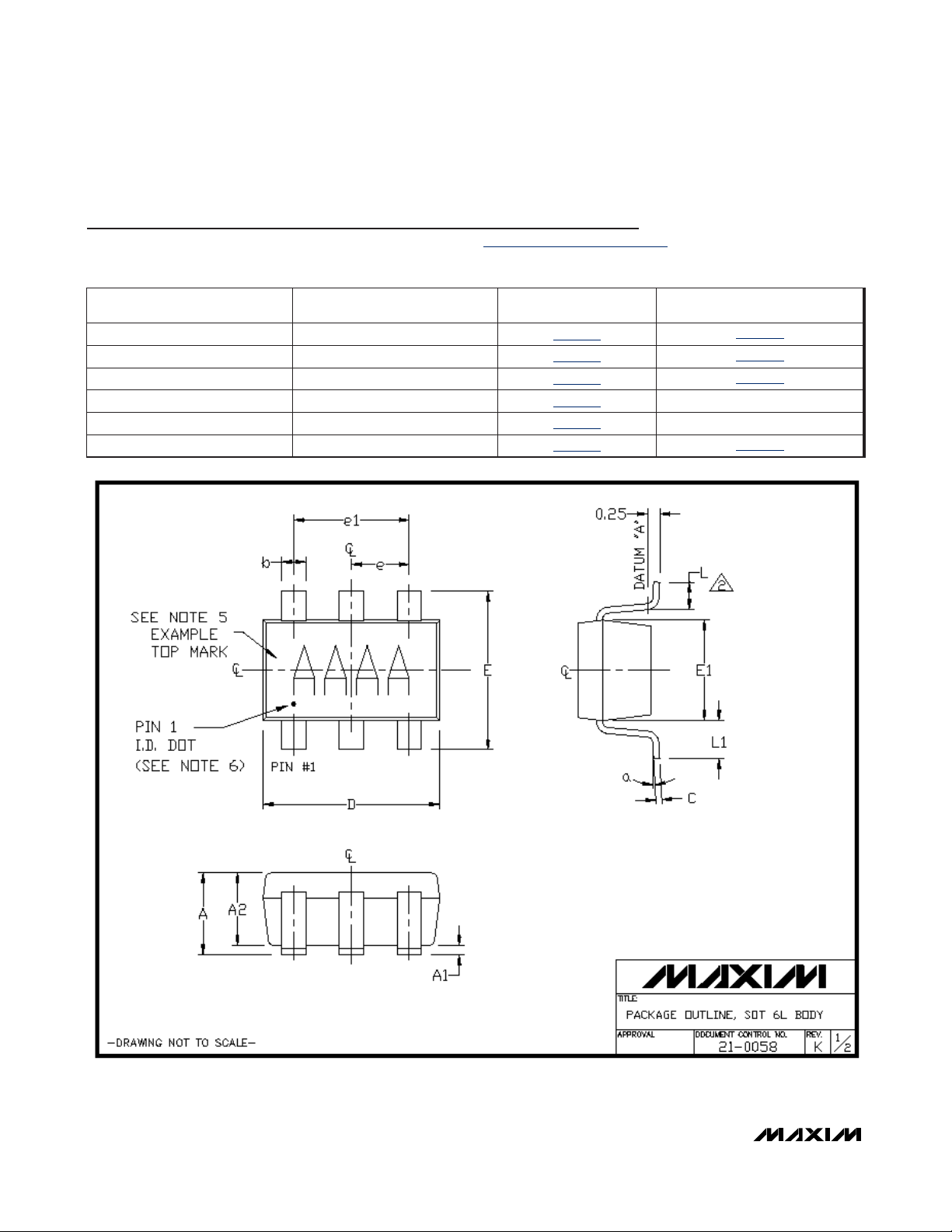
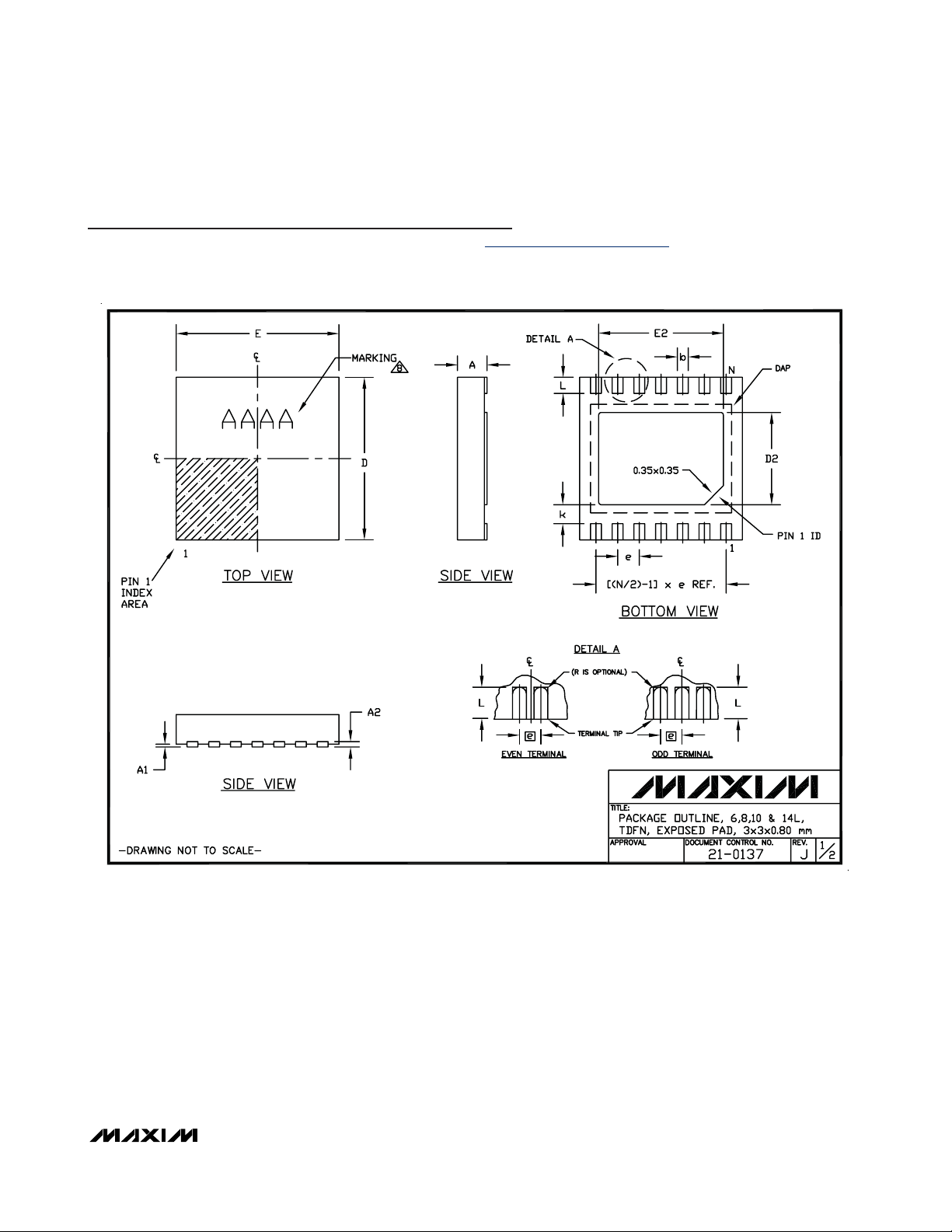
PACKAGE TYPE PACKAGE CODE OUTLINE NO.
LAND
PATTERN NO.
6 SOT23 U6F-6
21-0058
90-0175
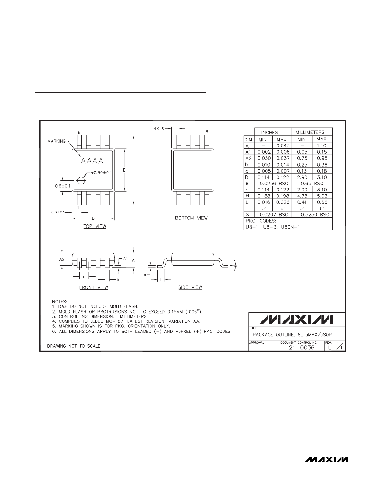
8 µMAX U8-1
21-0036
90-0092
14 TSSOP U14-2
21-0066
90-0117
8 SO S8-4
21-0041
—
14 SO S14-4
21-0041
—
6 TDFN-EP T633-2
21-0137
90-0058
Package Information
For the latest package outline information and land patterns, go to www.maxim-ic.com/packages. Note that a “+”, “#”, or “-” in the
package code indicates RoHS status only. Package drawings may show a different suffix character, but the drawing pertains to the
package regardless of RoHS status.

MAX4475–MAX4478/MAX4488/MAX4489
SOT23, Low-Noise, Low-Distortion,
Wide-Band, Rail-to-Rail Op Amps
______________________________________________________________________________________ 15
Package Information (continued)
For the latest package outline information and land patterns, go to www.maxim-ic.com/packages. Note that a “+”, “#”, or “-” in the
package code indicates RoHS status only. Package drawings may show a different suffix character, but the drawing pertains to the
package regardless of RoHS status.
MAX4475–MAX4478/MAX4488/MAX4489
SOT23, Low-Noise, Low-Distortion,
Wide-Band, Rail-to-Rail Op Amps
16 ______________________________________________________________________________________
α
α

MAX4475–MAX4478/MAX4488/MAX4489
SOT23, Low-Noise, Low-Distortion,
Wide-Band, Rail-to-Rail Op Amps
______________________________________________________________________________________ 17
Package Information (continued)
For the latest package outline information and land patterns, go to www.maxim-ic.com/packages. Note that a “+”, “#”, or “-” in the
package code indicates RoHS status only. Package drawings may show a different suffix character, but the drawing pertains to the
package regardless of RoHS status.
MAX4475–MAX4478/MAX4488/MAX4489
SOT23, Low-Noise, Low-Distortion,
Wide-Band, Rail-to-Rail Op Amps
18 ______________________________________________________________________________________
MAX4475–MAX4478/MAX4488/MAX4489
SOT23, Low-Noise, Low-Distortion,
Wide-Band, Rail-to-Rail Op Amps
______________________________________________________________________________________ 19
Package Information (continued)
For the latest package outline information and land patterns, go to www.maxim-ic.com/packages. Note that a “+”, “#”, or “-” in the
package code indicates RoHS status only. Package drawings may show a different suffix character, but the drawing pertains to the
package regardless of RoHS status.

MAX4475–MAX4478/MAX4488/MAX4489
SOT23, Low-Noise, Low-Distortion,
Wide-Band, Rail-to-Rail Op Amps
20 ______________________________________________________________________________________
Package Information (continued)
For the latest package outline information and land patterns, go to www.maxim-ic.com/packages. Note that a “+”, “#”, or “-” in the
package code indicates RoHS status only. Package drawings may show a different suffix character, but the drawing pertains to the
package regardless of RoHS status.
COMMON DIMENSIONS
SYMBOL
MIN. MAX.
A 0.70 0.80
D 2.90 3.10
E 2.90 3.10
0.00 0.05
A1
L0.20
A2 0.20 REF.
0.40
0.25 MIN.k
PACKAGE VARIATIONS
PKG. CODE
T633-2
T833-2
T833-3
T1033-1
T1033MK-1
T1033-2
T1433-1
N D2
6
1.50±0.10 2.30±0.10 0.95 BSC MO229 / WEEA 0.40±0.05 1.90 REF
8 1.50±0.10 2.30±0.10
8 1.50±0.10 2.30±0.10
10
1.50±0.10
1.50±0.10
10
10
1.70±0.10 2.30±0.1014
14
E2 e
2.30±0.10
2.30±0.10
2.30±0.10
2.30±0.101.70±0.10
2.30±0.101.70±0.10
JEDEC SPEC
0.65 BSC
0.65 BSC
0.50 BSC
0.50 BSC MO229 / WEED-3
0.40 BSC
0.40 BSC
0.40 BSC
MO229 / WEEC
MO229 / WEEC
MO229 / WEED-3
MO229 / WEED-3
- - - -
- - - -
b
[(N/2)-1] x e
0.30±0.05 1.95 REF
0.30±0.05 1.95 REF
2.00 REF0.25±0.05
0.25±0.05 2.00 REF
0.25±0.050.50 BSC1.50±0.10
0.20±0.05
0.20±0.05 2.40 REFT1433-3F
2.00 REF
2.40 REF0.20±0.05- - - -
2.40 REFT1433-2 14
MAX4475–MAX4478/MAX4488/MAX4489
SOT23, Low-Noise, Low-Distortion,
Wide-Band, Rail-to-Rail Op Amps
Maxim cannot assume responsibility for use of any circuitry other than circuitry entirely embodied in a Maxim product. No circuit patent licenses are
implied. Maxim reserves the right to change the circuitry and specifications without notice at any time.
Maxim Integrated Products, 120 San Gabriel Drive, Sunnyvale, CA 94086 408-737-7600 ____________________
21
© 2010 Maxim Integrated Products Maxim is a registered trademark of Maxim Integrated Products, Inc.
Revision History
REVISION
NUMBER
4 12/09
5 7/10 Added /V designation to the MAX4475 product and soldering temperature 1, 2
REVISION
DATE
DESCRIPTION
Added lead-free designations and an automotive part to the Ordering Information
and added input current spec in Absolute Maximum Ratings section
PAGES
CHANGED
1, 2, 13
 Loading...