

Page 1
For price, delivery, and to place orders, please contact Maxim Distribution at 1-888-629-4642,
or visit Maxim’s website at www.maxim-ic.com.
General Description
The MAX4480–MAX4483 low-cost, general-purpose op
amps offer Rail-to-Rail®outputs, draw only 50µA of quiescent current, and operate from a single +2.5V to +5.5V
supply. For additional power conservation, the MAX4481
offers a low-power shutdown mode that reduces supply
current to 0.5µA (max) and puts the amplifier’s output in a
high-impedance state. These devices are unity-gain stable with capacitive loads up to 400pF. The MAX4480–
MAX4483 are specified to +125°C, making them suitable
for use in a variety of harsh environments, such as automotive applications.
The MAX4480 is a single amplifier offered in a tiny 5-pin
SC70 package. The MAX4481 is a single amplifier with
a low-power shutdown mode that reduces supply current to <0.5µA and comes in a 6-pin SC70 package.
The MAX4482 is a dual amplifier and comes in the
space-saving 8-pin SOT23 package. The MAX4483 is a
quad amplifier and comes in a 14-pin TSSOP package.
All devices are specified for operation across the -40°C
to +125°C automotive temperature range.
Applications
Single-Supply Zero-Crossing Detectors
Instruments and Terminals
Portable Communications
Electronic Ignition Modules
Infrared Receivers
Sensor Signal Detection
Features
♦ Single +2.5V to +5.5V Supply Voltage Range
♦ 50µA Quiescent Current per Amplifier
♦ 0.5µA (max) Shutdown Mode (MAX4481)
♦ Available in Space-Saving Packages
5-Pin SC70 (MAX4480)
6-Pin SC70 (MAX4481)
8-Pin SOT23 (MAX4482)
♦ 105dB A
VOL
with 5kΩ Load
♦ 0.005% THD with 100kΩ Load
♦ Rail-to-Rail Output Voltage Swing
♦ 3.0mA of Sink and Source Load Current
♦ Unity-Gain Stable up to C
LOAD
= 400pF
MAX4480–MAX4483
Single/Dual/Quad, Low-Cost, Single-Supply,
Rail-to-Rail Op Amps with Shutdown
________________________________________________________________ Maxim Integrated Products 1
19-1809; Rev 1; 1/01
Pin Configurations
Selector Guide
MAX4481 1 Yes
MAX4482 2 No
MAX4483 4 No
Rail-to-Rail is a registered trademark of Nippon Motorola, Ltd.
Pin Configurations continued at end of data sheet.
No1MAX4480
PART
NO. OF AMPLIFIERS
PER PACKAGE
SHUTDOWN
MODE
Ordering Information
PART TEMP. RANGE
MAX4480AXK-T -40°C to +125°C
MAX4480AUK-T -40°C to +125°C
MAX4481AXT-T -40°C to +125°C
MAX4481AUT-T -40°C to +125°C
M A X4 4 8 2 AKA- T -40°C to +125°C
MAX4482ASA -40°C to +125°C
MAX4482AUA -40°C to +125°C
MAX4483ASD -40°C to +125°C
MAX4483AUD -40°C to +125°C
PIN-
PACKAGE
5 SC70 ABU
5 SOT23 ADPJ
6 SC70 AAN
6 SOT23 AAOS
8 SOT23 AAEJ
8 SO —
8 µMAX —
14 SO —
14 TSSOP —
TOP
M ARK
IN+
MAX4480 MAX4481
1
V
2
SS
IN-
3
SC70-5/SOT23-5 SC70-6/SOT23-6
VDDIN+
5
4
OUT
1
V
2
SS
IN-
3
V
6
DD
SHDN
5
OUT
4
Page 2
MAX4480–MAX4483
Single/Dual/Quad, Low-Cost, Single-Supply,
Rail-to-Rail Op Amps with Shutdown
2 _______________________________________________________________________________________
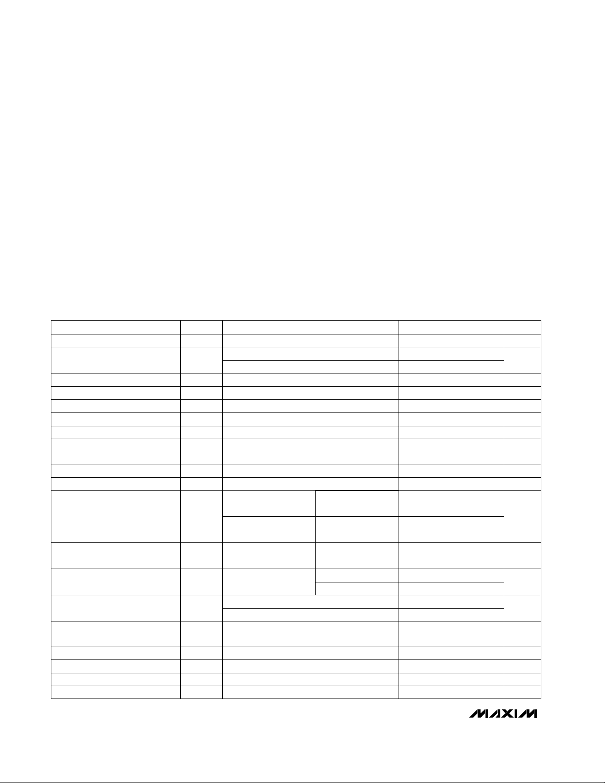
ABSOLUTE MAXIMUM RATINGS
ELECTRICAL CHARACTERISTICS
(VDD= +5V, VSS= 0, VCM= 0, V
OUT
= VDD/2, RL≥ 1MΩ connected to VDD/2, SHDN = VDD(MAX4481 only), TA= +25°C, unless
otherwise noted.)
Stresses beyond those listed under “Absolute Maximum Ratings” may cause permanent damage to the device. These are stress ratings only, and functional
operation of the device at these or any other conditions beyond those indicated in the operational sections of the specifications is not implied. Exposure to
absolute maximum rating conditions for extended periods may affect device reliability.
Power-Supply Voltage (VDDto VSS) .........................-0.3V to +6V
All Other Pins ...................................(VSS- 0.3V) to (VDD+ 0.3V)
Output Short-Circuit Duration
(OUT shorted to VSSor VDD)................................. Continuous
Continuous Power Dissipation (T
A
= +70°C)
5-Pin SC70 (derate 3.1mW/°C above +70°C)............. 247mW
6-Pin SC70 (derate 3.1mW/°C above +70°C)..............245mW
5-Pin SOT23 (derate 7.1mW/°C above +70°C)............571mW
6-Pin SOT23 (derate 8.7mW/°C above +70°C)............696mW
8-Pin SOT23 (derate 9.1mW/°C above +70°C)............727mW
8-Pin µMAX (derate 4.5mW/°C above +70°C) ............ 362mW
8-Pin SO (derate 5.88mW/°C above +70°C)............... 471mW
14-Pin TSSOP (derate 9.03mW/°C above +70°C) .......727mW
14-Pin SO (derate 8.33mW/°C above +70°C)............. 667mW
Operating Temperature Range .........................-40°C to +125°C
Junction Temperature ........................................................150°C
Storage Temperature Range .............................-65°C to +150°C
Lead Temperature (soldering, 10s) .................................+300°C
Output Short-Circuit Current
SHDN = VDDor VSS(MAX4481 only)
MAX4481 only
VDD= 5.0V
MAX4481 only
Device in shutdown mode, SHDN = VSS,
V
SS
< V
OUT
< VCC(MAX4481 only)
V
DD
= 2.5V
Sinking
Inferred from PSRR test
Sourcing
Specified as
V
OUT
- V
SS
2.5V ≤ VDD≤ 5.5V
VSS≤ VCM≤ VDD- 1.3V
Specified as
VDD- V
OUT
Inferred from CMRR test
Differential or common mode
SHDN = VSS(MAX4481 only)
(Note 1)
dB
(Note 1)
VSS+ 0.02V ≤ V
OUT
≤ VDD- 0.03V
CONDITIONS
kHz
140
GBWGain-Bandwidth Product
nA
±0.001 ±1 ±500
IIL, I
IH
SHDN Input Current
V
0.7 ✕V
DD
V
IH
SHDN Logic High
V
0.3 ✕V
DD
V
IL
SHDN Logic Low
µA
±0.01 ±0.1
I
OUTSHDN
Shutdown Mode Output Leakage
17
mA
3
I
SC
830
mV
1
V
OL
Output Voltage Low
80 150
mV
4
V
OH
Output Voltage High
110
50 100
RL= 100kΩ
µA
45
I
DD
V
2.5 5.5
V
DD
Supply Voltage Range
Supply Current per Amplifier
82 92
PSRRPower-Supply Rejection Ratio
dB
71 86
CMRRCommon-Mode Rejection Ratio
V
V
SS
VDD- 1.3
V
CM
Input Common-Mode Voltage
Range
MΩ
1000
R
IN
Input Resistance
µA
0.05 0.5
I
SHDN
Supply Current in Shutdown
mV
±1 ±5.5
V
OS
Input Offset Voltage
pA
±0.1 ±100
I
B
Input Bias Current
pA
±0.1 ±100
I
OS
Input Offset Current
UNITS
MIN TYP MAX
SYMBOLPARAMETER
RL= 100kΩ
RL= 5kΩ
RL= 100kΩ
RL= 5kΩ
VSS+ 0.10V ≤ V
OUT
≤ VDD- 0.20V
94 105
dBA
VOL
Large-Signal Voltage Gain
RL= 5kΩ
Page 3
MAX4480–MAX4483
Single/Dual/Quad, Low-Cost, Single-Supply,
Rail-to-Rail Op Amps with Shutdown
_______________________________________________________________________________________ 3
ELECTRICAL CHARACTERISTICS (continued)
(VDD= +5V, VSS= 0, VCM= 0, V
OUT
= VDD/2, RL≥ 1MΩ connected to VDD/2, SHDN = VDD(MAX4481 only), TA= +25°C, unless
otherwise noted.)
ELECTRICAL CHARACTERISTICS
(VDD= +5V, VSS= 0, VCM= 0, V
OUT
= VDD/2, RL≥ 1MΩ connected to VDD/2, SHDN = VDD(MAX4481 only), TA= -40°C to +125°C,
unless otherwise noted.) (Note 2)
Note 1: Guaranteed by design.
Note 2: Specifications are 100% tested at T
A
= +25°C (exceptions noted). All temperature limits are guaranteed by design.
Phase Margin
φ
M
70 degrees
Input Current Noise Density i
n
1
fA/√Hz
Capacitive-Load Stability C
LOAD
400
pF
Shutdown Delay Time t
SHDN
0.4
µs
Enable Delay Time t
EN
12
µs
Power-On Time t
ON
15
µs
Input Capacitance C
IN
2.0
pF
THD %
0.005
Settling Time to 0.1% t
S
50
µs
MAX4481 only
f = 10kHz
f = 1kHz, V
OUT
=
2Vp-p, AV= +1V/V
AV= +1V/V
MAX4481 only
V
OUT
= 2V step
PARAMETER SYMBOL
MIN TYP MAX
UNITSCONDITIONS
RL= 100kΩ
Total Harmonic Distortion
Input Voltage Noise Density e
n
100
nV/√Hz
f = 10kHz
Gain Margin 30 dB
Slew Rate SR 80 V/ms
Input Offset Voltage Drift TC
VOS
±3
µV/°C
Output Voltage Low V
OL
Specified as V
OUT
- VSS, RL = 5kΩ
50
mV
mV
200
Specified as VDD- V
OUT
, RL= 5kΩV
OH
Output Voltage High
Large-Signal Voltage Gain A
VOL
VSS+ 0.1V ≤ V
OUT
≤ VDD- 0.20V, RL= 5kΩ
84
dB
µA
1
SHDN = VDDor VSS(Note 1) (MAX4481 only)
I
IL,IIH
SHDN Input Current
SHDN Logic High
V
IH
MAX4481 only
0.7 ✕V
DD
V
V
0.3 ✕V
DD
MAX4481 onlyV
IL
SHDN Logic Low
±0.5
dB
77
2.5V ≤ VCC≤ 5.5VPSRRPower-Supply Rejection Ratio
Common-Mode Rejection Ratio CMRR V
SS
≤ VCM≤ VDD- 1.4V
67
dB
V
V
SS
V
DD
- 1.4
Inferred from CMRR testV
CM
Input Common-Mode Voltage
Range
Input Offset Current I
OS
(Note 1)
±100
pA
pA
±100
(Note 1)I
B
Input Bias Current
Input Offset Voltage V
OS
9
mV
Supply Current per Amplifier I
DD
120
µA
V
2.5 5.5
Inferred from PSRR testV
DD
Supply Voltage Range
PARAMETER SYMBOL CONDITIONS
MIN TYP MAX
UNITS
-40°C to +85°C
Shutdown Mode Output Leakage I
OUTSHDN
Device in shutdown
mode, SHDN = V
SS
,
V
SS
< V
OUT
< V
CC
(MAX4481 only)
±2.5
µA
+85°C to +125°C
Supply Current in Shutdown I
SHDN
SHDN = VSS, (MAX4481 only)
1.0
µA
Page 4
MAX4480–MAX4483
Single/Dual/Quad, Low-Cost, Single-Supply,
Rail-to-Rail Op Amps with Shutdown
4 _______________________________________________________________________________________
GAIN
(dB)/PHASE
(d
)
)
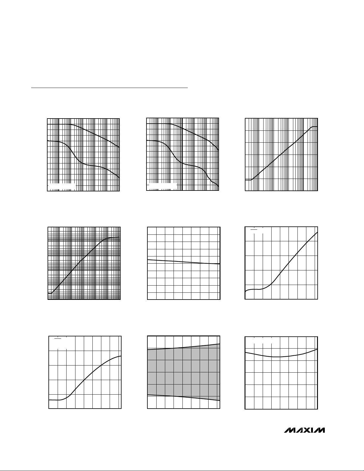
Typical Operating Characteristics
(VDD= +5V, VSS= 0, VCM= VDD/2, V
SHDN
= 5V, RL≥ 1MΩ connected to VDD/2, TA= +25°C, unless otherwise noted.)
GAIN AND PHASE
vs. FREQUENCY (NO LOAD)
80
60
40
20
0
egrees
-20
-40
-60
-80
-100
-120
-140
-160
A
= +1000V/V
VCL
-180
110 1k 1M100k
100 10k
FREQUENCY (Hz)
80
60
40
MAX4480 toc01
20
0
-20
-40
-60
-80
-100
GAIN (dB)/PHASE (degrees)
-120
-140
-160
-180
110
GAIN AND PHASE
vs. FREQUENCY (C
A
= +1000V/V
VCL
100
FREQUENCY (Hz)
1k 1M100k10k
= 400pF)
L
MAX4480 toc02
POWER-SUPPLY REJECTION RATIO
10
-10
-30
-50
PSRR (dB)
-70
-90
-110
10 1k100 10k 100k 1M
vs. FREQUENCY
FREQUENCY (Hz)
OUTPUT IMPEDANCE
vs. FREQUENCY
1000
100
10
1
OUTPUT IMPEDANCE (Ω)
0.1
0.01
1 10 100 1k 10k 100k
FREQUENCY (Hz)
MAX4481
OUTPUT LEAKAGE CURRENT
vs. TEMPERATURE
1000k
V
= V
SHDN
SS
V
OUT = VDD/2
100k
10k
(pA)
LEAK
I
1k
1M
MAX4480 toc4
MAX4480 toc07
SUPPLY CURRENT vs. TEMPERATURE
60
58
56
54
52
50
48
46
SUPPLY CURRENT (µA)
44
42
40
-40 0
-20 20
40 80
TEMPERATURE (°C)
INPUT OFFSET VOLTAGE
vs. TEMPERATURE
1500
1000
500
(µV)
0
OS
V
-500
60 100 120
100k
MAX4480 toc05
SUPPLY CURRENT (pA)
MAX4480 toc08
(mV)
OUT
- V
DD
V
SHUTDOWN SUPPLY CURRENT
vs. TEMPERATURE
V
= V
SHDN
SS
10k
1k
100
10
1
-40 0 40 80-20 20 60 100 120
TEMPERATURE (°C)
OUTPUT VOLTAGE SWING HIGH
vs. TEMPERATURE
100
RL = 5kΩ to VDD/2
90
80
70
60
MAX4480 toc03
MAX4481
MAX4480 toc06
MAX4480 toc09
100
10
-40 0 40 80-20 20 60 100 120
TEMPERATURE (°C)
-1000
-1500
-40 0 40 80-20 20 60 100 120
TEMPERATURE (°C
50
40
-40 0 40 80-20 20 60 100 120
TEMPERATURE (°C)
Page 5

MAX4480–MAX4483
Single/Dual/Quad, Low-Cost, Single-Supply,
Rail-to-Rail Op Amps with Shutdown
_______________________________________________________________________________________ 5
Typical Operating Characteristics (continued)
(VDD= +5V, VSS= 0, VCM= VDD/2, V
SHDN
= 5V, RL≥ 1MΩ connected to VDD/2, TA= +25°C, unless otherwise noted.)
OUTPUT VOLTAGE SWING LOW
vs. TEMPERATURE
11
RL = 5kΩ to VDD/2
10
9
8
(mV)
SS
- V
7
OUT
V
6
5
4
-40 0 40 80-20 20 60 100 120
TEMPERATURE (°C)
LARGE-SIGNAL GAIN
vs. TEMPERATURE
110
RL = 5kΩ to VDD/2
105
100
GAIN (dB)
95
90
-40 0 40 80-20 20 60 100 120
TEMPERATURE (°C)
COMMON-MODE REJECTION RATIO
vs. TEMPERATURE
TEMPERATURE (°C)
MINIMUM OPERATING VOLTAGE
vs. TEMPERATURE
TEMPERATURE (°C)
MAX4480 toc11
MAX4480 toc14
130
RL = 5kΩ to VDD/2
125
120
115
110
105
GAIN (dB)
100
95
90
85
80
0.5 1.5 2.5 3.51.0 2.0 3.0 4.0 4.5
TOTAL HARMONIC DISTORTION
PLUS NOISE vs. FREQUENCY
100
RL = 5kΩ
= 2Vp-p
V
OUT
= +1
A
10
V
BW = 30kHz
1
THD + N (%)
0.1
0.01
0.001
10 1k100 10k 100k
MAX4480 toc10
MAX4480 toc13
-80
-82
-84
CMRR (dB)
-86
-88
-90
-40 0 40 80-20 20 60 100 120
2.0
1.9
1.8
1.7
1.6
(MIN)
1.5
DD
V
1.4
1.3
1.2
1.1
1.0
-40 0 40 80-20 20 60 100 120
LARGE-SIGNAL GAIN
vs. OUTPUT VOLTAGE
V
(V)
OUT
FREQUENCY (Hz)
MAX4480 toc12
MAX4480 toc15
TOTAL HARMONIC DISTORTION
PLUS NOISE vs. FREQUENCY
100
RL = 100kΩ
= 2Vp-p
V
OUT
= +1
A
10
V
BW = 30kHz
1
THD + N (%)
0.1
0.01
0.001
10 1k100 10k 100k
FREQUENCY (Hz)
MAX4480 toc16
TOTAL HARMONIC DISTORTION
PLUS NOISE vs. INPUT AMPLITUDE
100
RL = 5kΩ
f = 1kHz
10
BW = 22kHz
1
THD + N (%)
0.1
0.01
0.001
0213
VIN (Vp-p)
MAX4480 toc17
THD + N (%)
0.01
0.001
TOTAL HARMONIC DISTORTION
PLUS NOISE vs. INPUT AMPLITUDE
100
RL = 100kΩ
f = 1kHz
10
BW = 22kHz
1
0.1
0 1.00.5 1.5 2.0 2.5 3.0
VIN (Vp-p)
MAX4480 toc18
Page 6
MAX4480–MAX4483
Single/Dual/Quad, Low-Cost, Single-Supply,
Rail-to-Rail Op Amps with Shutdown
6 _______________________________________________________________________________________
Typical Operating Characteristics (continued)
(VDD= +5V, VSS= 0, VCM= VDD/2, V
SHDN
= 5V, RL≥ 1MΩ connected to VDD/2, TA= +25°C, unless otherwise noted.)
CAPACITIVE-LOAD STABILITY
20
0
1k 10k 100k
5
MAX4480 toc19
RESISTIVE LOAD (Ω)
CAPACITIVE LOAD (nF)
10
15
AV = +1V/V
T
A
= +25°C
R
L
// C
L
STABLE
REGION
UNSTABLE
REGION
NONINVERTING SMALL-SIGNAL
TRANSIENT RESPONSE
MAX4480 roc20
20µs/div
AV = 1V/V
R
L
= 5kΩ
IN
50mV/div
OUT
NONINVERTING LARGE-SIGNAL
TRANSIENT RESPONSE
MAX4480 roc21
100µs/div
AV = 1V/V
R
L
= 5kΩ
IN
1V/div
OUT
0
10
5
20
15
25
0 200 300100 400 500 600
PERCENT OVERSHOOT
vs. CAPACITIVE LOAD
MAX4480 toc22
C
LOAD
(pF)
OVERSHOOT (%)
POSITIVE
OVERSHOOT
NEGATIVE
OVERSHOOT
0
20
10
40
30
50
60
0231 456
SUPPLY CURRENT vs. SUPPLY VOLTAGE
MAX4480 toc24
SUPPLY VOLTAGE (V)
SUPPLY CURRENT (µA)
V
OUT
= VDD/2
20
50
40
80
70
60
110
100
90
120
10 1k100 10k 100k 1M
CHANNEL-TO-CHANNEL ISOLATION
vs. FREQUENCY
MAX4480 toc23
FREQUENCY (kHz)
CHANNEL-TO-CHANNEL ISOLATION (dB)
30
Page 7

MAX4480–MAX4483
Single/Dual/Quad, Low-Cost, Single-Supply,
Rail-to-Rail Op Amps with Shutdown
_______________________________________________________________________________________ 7
Pin Description
Detailed Description
Rail-to-Rail Output Stage
The MAX4480–MAX4483 can drive a 5kΩ load and still
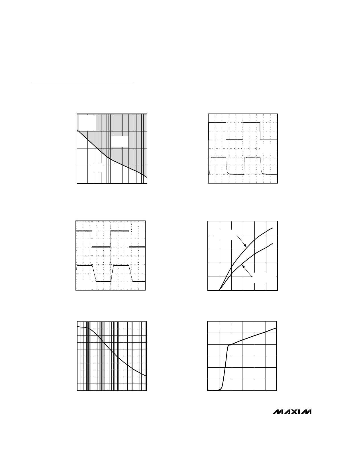
typically swing within 80mV of the supply rails. Figure 1
shows the MAX4480 output voltage swing configured
with AV = +10V/V.
Driving Capacitive Loads
Driving a capacitive load can cause instability in many
op amps, especially those with low quiescent current.
The MAX4480–MAX4483 are unity-gain stable for a
range of capacitive loads to above 400pF. Figure 2
shows the MAX4480 response with an excessive
capacitive load. Adding a series resistor between the
output and the load capacitor (Figure 3) improves the
Figure 1. Rail-to-Rail Output Operation
MAX4483
MAX4482
MAX4480
MAX4481
IN+——1 Noninverting Amplifier Input1
OUTC
OUTD
V
DD
SHDN
INC-
IND-
OUT
OUTA
OUTB
V
SS
IN-
INA-
INB-
IND+
INC+
INB+
INA+
NAME
8
14
4
—
9
13
—
1
7
11
—
2
6
12
10
5
3
PIN
—
—
8
—
—
—
—
1
7
4
—
2
6
—
—
5
3
Amplifier Output C——
Amplifier Output D——
Positive Supply. Use a 0.01µF bypass capacitor to GND.65
Active-Low Shutdown Input. Connect to VDDfor
normal operation. Do not leave floating.
5—
Inverting Amplifier Input C——
Inverting Amplifier Input D——
Amplifier Output44
Amplifier Output A——
Amplifier Output B——
Negative Supply. Connect to ground for single-supply
operation. Use a 0.01µF bypass capacitor to GND.
22
Inverting Amplifier Input33
Inverting Amplifier Input A——
Inverting Amplifier Input B——
Noninverting Amplifier Input D——
Noninverting Amplifier Input C——
Noninverting Amplifier Input B——
Noninverting Amplifier Input A——
FUNCTION
100µs/div
1V/div
Page 8

MAX4480–MAX4483
Single/Dual/Quad, Low-Cost, Single-Supply,
Rail-to-Rail Op Amps with Shutdown
8 _______________________________________________________________________________________
circuit’s response by isolating the load capacitance
from the op amp’s output.
Applications Information
Shutdown Mode
The MAX4481 features a low-power shutdown mode.
When SHDN goes low, the supply current drops to
0.05µA (typ) and the output enters a high-impedance
state. Pull SHDN high to enable the amplifier. Do not
leave SHDN floating. Figure 4 shows the shutdown
waveform.
Power-Up
The MAX4480–MAX4483 outputs typically settle within
50µs after power-up. Figure 5 shows the output voltage
on power-up and power-down.
Power Supplies and Layout
The MAX4480–MAX4483 operate from a single +2.5V to
+5.5V power supply. Bypass the power supply with a
0.1µF capacitor to ground.
Good layout techniques optimize performance by
decreasing the amount of stray capacitance at the op
amp’s inputs and outputs. To decrease stray capacitance, minimize trace lengths by placing external components close to the op amp’s pins.
Chip Information
MAX4480/MAX4481 TRANSISTOR COUNT: 111
MAX4482 TRANSISTOR COUNT: 209
MAX4483 TRANSISTOR COUNT: 407
Figure 3. Capacitive-Load-Driving Circuit
Figure 4. Shutdown Waveform
Figure 5. Power-Up/Down Waveform
Figure 2. Small-Signal Transient Response with Excessive
Capacitive Load
R
ISO
CL = 1nF
50mV/div
MAX4480
MAX4481
MAX4482
MAX4483
20µs/div
C
L
2V/div
RL = 10MΩ TO VSS, CL = 25pF
400µs/div
V
DD
2V/div
OUT
1V/div
4µs/div
Page 9

MAX4480–MAX4483
Single/Dual/Quad, Low-Cost, Single-Supply,
Rail-to-Rail Op Amps with Shutdown
_______________________________________________________________________________________ 9
Pin Configurations (continued)
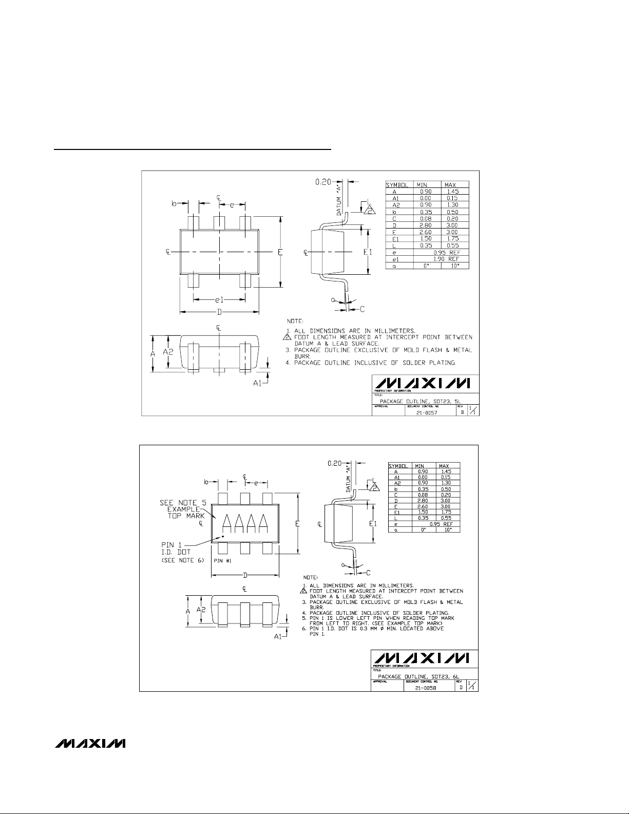
Package Information
OUTA
INA-
INA+
V
1
2
3
4
SS
SOT23-8/SO/µMAX
MAX4482
MAX4483
OUTA
1
INA-
2
V
8
DD
3
INA+
OUTB
7
4
V
DD
INB-
6
5
INB+
INB+
5
6
INB-
7
OUTB
OUTD
14
IND-
13
IND+
12
11
V
SS
10
INC+
9
INC-
OUTC
8
TSSOP/SO
SC70, 5L.EPS
Page 10

MAX4480–MAX4483
Single/Dual/Quad, Low-Cost, Single-Supply,
Rail-to-Rail Op Amps with Shutdown
10 ______________________________________________________________________________________
Package Information (continued)
SC70, 6L.EPS
SOT23, 8L.EPS
Page 11
MAX4480–MAX4483
Single/Dual/Quad, Low-Cost, Single-Supply,
Rail-to-Rail Op Amps with Shutdown
______________________________________________________________________________________ 11
Package Information (continued)
SOT5L.EPS
6LSOT.EPS
Page 12

Package Information (continued)
MAX4480–MAX4483
Single/Dual/Quad, Low-Cost, Single-Supply,
Rail-to-Rail Op Amps with Shutdown
12 ______________________________________________________________________________________
8LUMAXD.EPS
Page 13

Maxim cannot assume responsibility for use of any circuitry other than circuitry entirely embodied in a Maxim product. No circuit patent licenses are
implied. Maxim reserves the right to change the circuitry and specifications without notice at any time.
13 ____________________Maxim Integrated Products, 120 San Gabriel Drive, Sunnyvale, CA 94086 408-737-7600
© 2001 Maxim Integrated Products Printed USA is a registered trademark of Maxim Integrated Products.
Single/Dual/Quad, Low-Cost, Single-Supply,
Rail-to-Rail Op Amps with Shutdown
MAX4480–MAX4483
Package Information (continued)
TSSOP,NO PADS.EPS
 Loading...