For free samples & the latest literature: http://www.maxim-ic.com, or phone 1-800-998-8800.
For small orders, phone 1-800-835-8769.
General Description
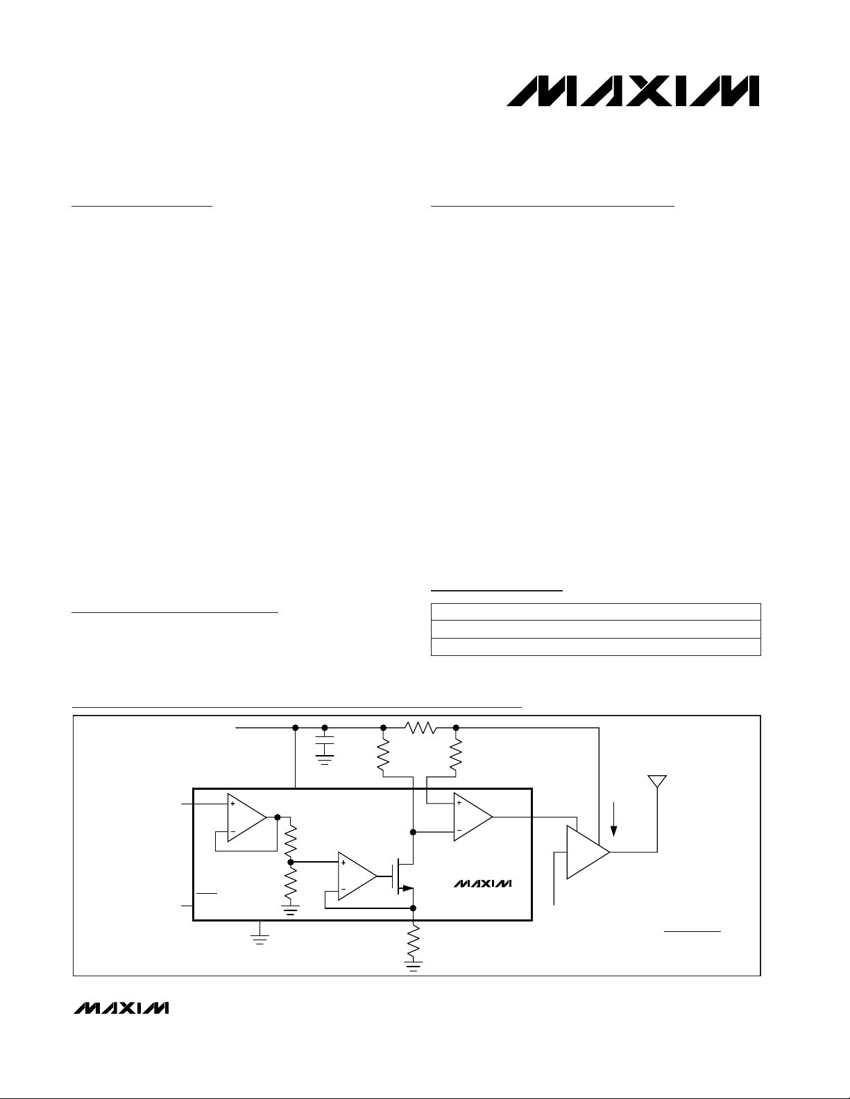
The MAX4473 PA power control IC is intended for
closed-loop bias control of GSM power amplifiers. The
device facilitates accurate control of the current delivered to the power amplifier (PA) via a control voltage.
The error amplifier senses the voltage drop across an
external current-sense resistor placed between the
supply and the PA. The output of the error amplifier
adjusts the PA gain until the current is proportional to
the power control voltage applied to the MAX4473. This
unique topology is useful in time-division-multipleaccess (TDMA) systems, such as GSM, where accurate
transmit burst shaping and power control is required.
User-selectable current sensing and gain setting resistors maximize flexibility.
The MAX4473 operates from a single +2.7V to +6.5V
supply and typically draws 1.2mA of supply current.
The error amplifier has a common-mode range that
extends from +1V to VCC. The power control input and
error amplifier outputs swing Rail-to-Rail®. A low-power
shutdown mode reduces supply current to less than
1µA and activates an on-board active pull-down at the
error amplifier output. Fast enable/disable times of
0.9µs reduce average power consumption without compromising dynamic performance. The MAX4473 is
available in a space-saving 8-pin µMAX package.
Applications
GSM Cellular Phones
Cordless Phones
Precision Current Control
High-Frequency Servo Loops
Features
♦ Optimized for GSM Timing Requirements
♦ +2.7V to +6.5V Single-Supply Operation
♦ 1.2mA Supply Current
♦ ≤1µA Supply Current in Shutdown Mode
♦ Guaranteed 1.5µs Enable/Disable Times
♦ Active Output Pull-Down in Shutdown Mode
♦ Rail-to-Rail Error Amplifier Output
♦ Rail-to-Rail Power Control Input
♦ Output Drive Capability—500Ω and 300pF Loads
♦ +1V to V
CC
Current Sense Input Common-Mode
Voltage Range
♦ No Phase-Reversal for Common-Mode Voltage
from 0 to V
CC
♦ External Current Sensing and Gain Setting
Resistors Maximize Flexibility
♦ Available in a Space-Saving 8-pin µMAX
MAX4473
Low-Cost, Low-Voltage, PA Power Control
Amplifier for GSM Applications in 8-Pin µMAX
________________________________________________________________
Maxim Integrated Products
1
GND
PC
0.1µF
8
7
R
3R
A3
PA
GC
IN
RFIN
4
3
SHDN
BUFFER
5
6
A2
Q1
A1
12
SR1 SR2
SR3
RG3
OUT
V-TO-I
CONVERTER
ERROR
AMPLIFIER
V
CC
V
CC
V
CC
R
SENSE
RG1 RG2
I
CCPA
MAX4473
4 · RG3 · R
SENSE
V
PC
· RG1
I
CCPA
=
Typical Operating Circuit
19-1448; Rev 0; 3/99
PART
MAX4473EUA
MAX4473ESA -40°C to +85°C
-40°C to +85°C
TEMP. RANGE PIN-PACKAGE
8 µMAX
8 SO
Pin Configuration appears at end of data sheet.
Ordering Information
Rail-to-Rail is a registered trademark of Nippon Motorola, Ltd.

MAX4473
Low-Cost, Low-Voltage, PA Power Control
Amplifier for GSM Applications in 8-Pin µMAX
2 _______________________________________________________________________________________
ABSOLUTE MAXIMUM RATINGS
ELECTRICAL CHARACTERISTICS
(VCC= +2.7V to +6.5V, SHDN > +2.4V, MAX4473 test circuit, RG1 = RG2 = 1kΩ ±1%, RG3 = 2.5kΩ ±1%, R
SENSE
= 100Ω ±1%, R
L
= 10kΩ, CL= 300pF, TA= T
MIN
to T
MAX
, unless otherwise noted. Typical values are at VCC= +6.0V, VPC= +1.0V, TA= +25°C.)
(Note 1)
Stresses beyond those listed under “Absolute Maximum Ratings” may cause permanent damage to the device. These are stress ratings only, and functional
operation of the device at these or any other conditions beyond those indicated in the operational sections of the specifications is not implied. Exposure to
absolute maximum rating conditions for extended periods may affect device reliability.
VCCto GND ...........................................................................+7V
SR1, SR2, SR3, PC, SHDN,
OUT to GND............................................-0.3V to (V
CC
+ 0.3V)
SR1 to SR3......................................................................0 to V
CC
OUT and SR3 Short-Circuit Duration
to V
CC
or GND ........................................................Continuous
Current into Any Pin..........................................................±50mA
Continuous Power Dissipation (T
A
= +70°C)
µMAX (derate 4.10mW/°C above +70°C) .....................330mW
SO (derate 5.88mW/°C above +70°C)..........................471mW
Operating Temperature Range ...........................-40°C to +85°C
Junction Temperature......................................................+150°C
Storage Temperature Range.............................-65°C to +150°C
Lead Temperature (soldering, 10sec).............................+300°C
V
OUT
= VCC/ 2
RL= 500Ω
to V
CC
/ 2
VPC= 0
2.7V < V
CC
< 6.5V, VPC= GND
1V < V
SR1
, V
SR2
< VCC,
VPC= GND
Inferred from CMRR test; VPC= GND (Note 2)
1V < V
SR1
, V
SR2
< V
CC
SHDN < 0.4V, V
SR1
= V
SR2
= V
CC
1V < V
SR1
, V
SR2
< V
CC
SHDN < 0.4V, RL= 10kΩ
1V < V
SR1
, V
SR2
< VCC, VPC= GND,
SR3 = unconnected
SHDN = 0 to V
CC
1V < V
SR1
, V
SR2
< VCC, VPC= GND,
SR3 = unconnected
CONDITIONS
mA20Output Current Limit
0.15 V
CC
-
0.15
80 120
80 130
80 125
dB
80 130
dB80 90Power-Supply Rejection Ratio
75 95
65 85
Common-Mode Rejection Ratio
µA±0.001 ±0.5SR1, SR2 Shutdown Leakage Current
µA±0.001 ±0.2SR1, SR2 Input Bias Offset Current
µA±0.04 ±1SR1, SR2 Input Bias Current
mA1.2 2Supply Current
V2.7 6.5Supply Voltage
V1V
CC
SR1, SR2 Input Common-Mode
Voltage Range
µV/°C
10SR1, SR2 Input Offset Voltage Drift
mV±0.5 ±2SR1, SR2 Input Offset Voltage
µA0.03 1Shutdown Supply Current
V2.4
SHDN Input High Voltage
V0.4
SHDN Input Low Voltage
µA±0.5
SHDN Input Current
UNITSMIN TYP MAXPARAMETER
VCC= 2.7V
VCC= 6.5V
VCC= 6.5V, 0.3V < V
OUT
< 6V
VCC= 2.7V, 0.3V < V
OUT
< 2.4V
RL= 10kΩ
to VCC/ 2
VCC= 6.5V, 0.7V < V
OUT
< 5.5V
VCC= 2.7V, 0.7V < V
OUT
< 2.2V
RL= 10kΩ, CL= 300pF
RL= 10kΩ, CL= 300pF, fo= 10kHz
degrees60Phase Margin
MHz
2Gain-Bandwidth Product
Measured from 30% to 70% of V
OUT
, RL= 10kΩ,
CL= 300pF
V/µs
1.8Slew Rate
Large Signal-Gain
RL= 10kΩ to VCC/ 2
RL= 500Ω to VCC/ 2
V
0.5 V
CC
-
0.5
Output Voltage Swing
dB
ERROR AMPLIFIER
GENERAL
 Loading...