19-0302; Rev 0; 9/94
Low-Cost, High-Resolution, 200MHz
Video CRT Driver
_______________General Description
The MAX445 is a high-performance, monolithic, variablegain transconductance amplifier with a high-voltage
open-collector output capable of directly driving a video
display (CRT cathode). A 2.5ns rise time is achieved
using a peaking network with a 200Ω load resistor and
an 8pF total load (CRT and parasitic capacitance).
Differential inputs and a linear adjustable gain stage
with an output offset adjustment make the versatile
MAX445 well suited for many video display applications. A buffered bandgap reference voltage is available for the gain (contrast) and offset adjustments
along with a TTL BLANK input to turn off the output current, independent of signal input.
The MAX445 is available in a 24-pin power-tab DIP
package. A suitable heatsink must be attached to
maintain the junction temperature within the recommended operating range.
________________________Applications
CRT Driver for High-Resolution Monochrome and
Color Displays
High-Voltage, Variable-Gain Transconductance
Amplifier
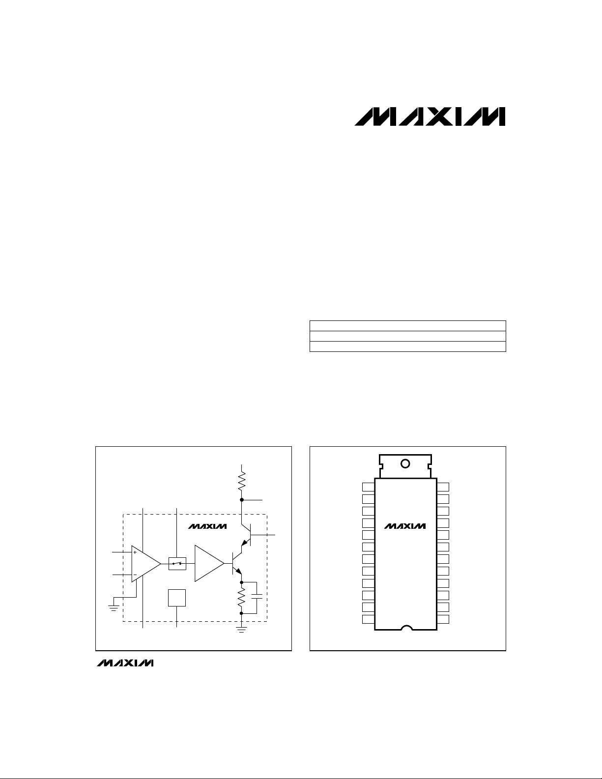
________________Functional Diagram
V
AA
____________________________Features
♦ 2.5ns Rise/Fall Time into an 8pF Load
♦ 200MHz Small-Signal Bandwidth
♦ 50Vp-p Output
♦ Ground Referenced Differential Inputs
♦ Linear Variable Gain for Contrast Control
♦ Offset Adjustment for Black Level
♦ 5.5V Bandgap Reference
♦ Drives 1280 x 1024 and 1530 x 1280 Displays
______________Ordering Information
PART
MAX445CPG
MAX445C/D 0°C to +70°C**
* Case temperature range, T
Maximum Ratings and Applications Information for thermal/heat
sink considerations.
**Dice are specified at TJ= +25°C, DC parameters only.
TEMP. RANGE PIN-PACKAGE
0°C to +70°C*
CASE
24 Power-Tab DIP
Dice
= 0°C to +90°C. See Absolute
__________________Pin Configuration
TOP VIEW
MAX445
R
VIN+
VIN-
GNDA
L
V
CONTRAST
BLANK
IOUT
MAX445
BAND
GAP
VREF
CURRENT
AMP
GND
PRE-AMP
OFFSET
________________________________________________________________
OUT
VCB
GND
VREF
OFFSET
CONTRAST
GNDA
VINVIN+
V
BLANK
GND
1
2
3
4
MAX445
5
6
7
V
EE
8
V
EE
9
CC
10
11
12
Power-Tab DIP
Maxim Integrated Products
Call toll free 1-800-998-8800 for free samples or literature.
GND
24
GND
23
GND
22
V
EEO
21
N.C.
20
IOUT
19
N.C.
18
VCB
17
VCB
16
GND
15
GND
14
GND
13
1

Low-Cost, High-Resolution, 200MHz
Video CRT Driver
ABSOLUTE MAXIMUM RATINGS
VAAOutput Supply.................................................................80V
Output Supply with Respect to VCB...............................70V
V
AA
VCB Common-Base Supply...................................................20V
Positive Supply............................................................12.5V
V
CC
Negative Supply..........................................................-12.5V
V
EE
Differential Input Voltage..........................................................2V
Common-Mode Input Voltage................................................±2V
MAX445
Contrast Input Voltage.................................................-1V to +6V
Stresses beyond those listed under “Absolute Maximum Ratings” may cause permanent damage to the device. These are stress ratings only, and functional
operation of the device at these or any other conditions beyond those indicated in the operational sections of the specifications is not implied. Exposure to
absolute maximum rating conditions for extended periods may affect device reliability.
ELECTRICAL CHARACTERISTICS
(VAA= 20V, VCB = 10V ±0.5V, VCC= 10V ±0.5V, VEE= -10.5V ±0.5V, VIN = (VIN+) - (VIN-) = 0V, CONTRAST = 1.0V,
OFFSET = 1.0V, R
Output-Common-Base Supply Current
Positive Supply Current
Negative Supply Current
Low Blank Input Bias Current
High Blank Input Bias Current
Contrast Input Bias Current
Offset Input Bias Current
VIN+ or VIN- Signal Input Current
VIN+ or VIN- DC Input Impedance
VIN+ or VIN- Input Capacitance
Reference Output Voltage
Output Current (Blanked)
Output Current
Output Current Change vs. Temperature
Output Current Change vs. Contrast ADJ
Output Current Change vs. VIN, Blanked
Amplifier Linearity Error (∆Gm/∆VIN)
Contrast Linearity Error (∆Gm/∆Contrast)
= 0Ω, BLANK = 0.4V, T
L
to VIN
OUT
= +25°C, unless otherwise noted.)
CASE
CB
CC
I
VEE
VCC, VEE= ±5%, VIN = +250mV,
CONTRAST = 5.0V, referred to input
BLANK = 0.4V
IL
BLANK = 2.4V
CONTRAST = 5.0V
OFFSET = 1.0V
VCM= ±0.5V, CONTRAST = 5.0V
IN
I
LOAD
BLANK = 2.4V, OFFSET = 1V, VAA= 75V
BLANK = 2.4V, OFFSET = 3V
OFFSET = 0V, CONTRAST = 4.0V
OFFSET = 5.0V, CONTRAST = 1V
TC= +25°C to +90°C
CONTRAST = 0V to 5V
BLANK = 2.4V, CONTRAST = 5.0V,
∆VIN- = 0.3V
CONTRAST = 5.0V
CONTRAST = 1.0V
CONTRAST = 0V
CONTRAST = 4.0V, OFFSET = 1.0V
VIN = 0.2V, OFFSET = 0V
OFFSET = 0V, R
∆I
∆I
∆I
I
OUT
I
OUT
GmTransconductance, I
EE
IH
IC
IB
IS
VIN
REF
OUT
OUT
OUT
Offset Input Voltage.....................................................-1V to +6V
Blank Input Voltage.....................................................-1V to +6V
Bandgap-Reference Output Current...................................-5mA
Continuous Power Dissipation
derate at 170mW/°C above T
Operating Junction Temperature ......................-55°C to +150°C
Storage Temperature.........................................-55°C to +150°C
Lead Temperature (soldering, 10sec).............................+300°C
CONDITIONS
+ I
VEEO
= 2mA
= 100Ω
LOAD
= +90°C.......................10W
CASE
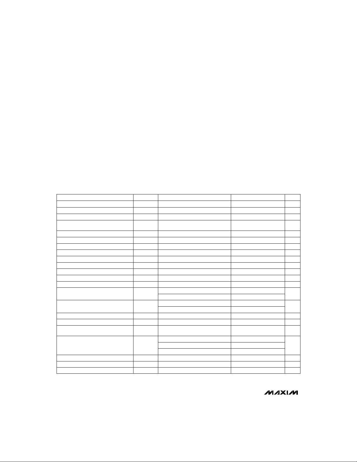
-0.1 25
80 140
400 600
70 120
-25 25
±1
±1
UNITSMIN TYP MAXSYMBOLPARAMETER
mA40I
mA70I
mA-100I
dB25PSRRPower-Supply Rejection Ratio
mA-0.6 0I
mA-0.4 0I
µA010I
µA010I
µA-50 50I
dB36CMRRInput Common-Mode Rejection Ratio
kΩ10R
pF2C
V5.25 5.75V
mA
mA
mA±3
mA±10
mA±1
mA/V
%±2
%±3
MHz200BWBandwidth, 3dB
2 _______________________________________________________________________________________

Low-Cost, High-Resolution, 200MHz
Video CRT Driver
ELECTRICAL CHARACTERISTICS (continued)
(VAA= 20V, VCB = 10V ±0.5V, VCC= 10V ±0.5V, VEE= -10.5V ±0.5V, VIN = (VIN+) - (VIN-) = 0V, CONTRAST = 1.0V,
OFFSET = 1.0V, R
Rise/Fall Time (10% to 90%)
Settling Time (90% to 100% ±2%)
= 0Ω, BLANK = 0.4V, T
L
= +25°C, unless otherwise noted.)
CASE
CONDITIONS
RL= 200Ω,
tr, t
CL= 8pF,
f
VAA= 75V,
tr(VIN) < 1ns,
CL= 8pF, no peaking
s
No peaking,
OUTp-p = 50V
With peaking,
OUTp-p = 45V
UNITSMIN TYP MAXSYMBOLPARAMETER
3.6
ns
2.5
ns8t
%±2Thermal Distortion
______________________________________________________________Pin Description
PIN
1, 12, 13, 14,
15, 22, 23, 24
2 VREF Reference Output (+5.5V)
3 OFFSET Output Voltage Offset-Adjustment Input
4 CONTRAST Output Gain-Adjustment Input
5 GNDA Pre-Amp Ground
6 VIN- Inverting Signal Input
7 VIN+ Noninverting Signal Input
8, 9 V
10 V
11 BLANK Blanking Input, TTL
16, 17 VCB Output Common-Base Supply (+10V)
18, 20 N.C. No Connection—leave open
19 IOUT Open-Collector Current Output
21 V
NAME FUNCTION
GND High-Current Ground. Connect all pins to ground plane.
EE
CC
EEO
Negative Supply (-10.5V)
Positive Supply (+10V)
Negative Supply for Output Stage (-10.5V)
MAX445
_______________________________________________________________________________________ 3
 Loading...