

General Description
The MAX4455 is an eight-channel arbitrary graphics
on-screen display (OSD) video generator that inserts
arbitrary gray-scale bit-mapped graphics into eight
asynchronous composite video sources. Ideal for security camera surveillance systems, the MAX4455 supports the insertion of graphics and text on up to eight
video output channels in 15 levels of brightness. It easily displays information such as company logo, camera
location, time, and date with arbitrary fonts and sizes.
Arbitrary graphics capability enables the display of
unique languages and fonts, allowing manufacturers to
tailor their system for any geographic market. The
MAX4455 is designed to work with Maxim’s video
crosspoint switches, such as the MAX4356 and
MAX4358, which include circuitry that simplifies the
insertion of the OSD information. The MAX4455 can
also be used with discrete fast mux switches.
The MAX4455 operates from a 3V to 3.6V digital supply, and a 2.7V to 5.5V analog supply. Independent
interface supplies enable the MAX4455 to communicate with microprocessors and OSD crosspoint switch
logic with logic levels ranging from 2.7V to 5.5V. The
MAX4455 uses an external 16Mb SDRAM for graphical
image storage for all eight video channels. The
MAX4455 manages all memory interface functions,
allowing a simple host µP interface. The MAX4455’s
multiple-channel memory sharing and multiple-location
write function allow fast memory updates of shared
graphics information necessary for rapidly changing
OSD information, such as a time stamp.
The MAX4455 is available in a thin 100-pin TQFP package (200mm2area), and is fully specified over the
extended temperature range (-40°C to +85°C). The
MAX4455EVSYS is available to evaluate the MAX4455
along with the MAX4358 (32 × 16 video crosspoint
switch with OSD).
Applications
Security Systems
Video Routing
Industrial Applications
Features
♦ Generates Arbitrary Graphics Images
♦ 15-Level Gray Scale
♦ 8 Channels of Bit-Mapped OSD
♦ Loss-of-Signal Detector for All Channels
♦ Graphics Updatable Within the Vertical Interval
♦ Update Time Stamp on All Eight Channels
Simultaneously
♦ 3V and 5V Single-Supply Operation
♦ Works with MAX4356/MAX4358 Video Crosspoint
Devices and Fast Mux Switches
♦ Small 100-Pin TQFP Package (200mm
2
)
MAX4455
Arbitrary Graphics On-Screen Display
Video Generator
________________________________________________________________ Maxim Integrated Products 1
Ordering Information
19-2463; Rev 2; 3/03
For pricing, delivery, and ordering information, please contact Maxim/Dallas Direct! at
1-888-629-4642, or visit Maxim’s website at www.maxim-ic.com.
EVALUATION KIT
AVAILABLE
Pin Configuration appears at end of data sheet.
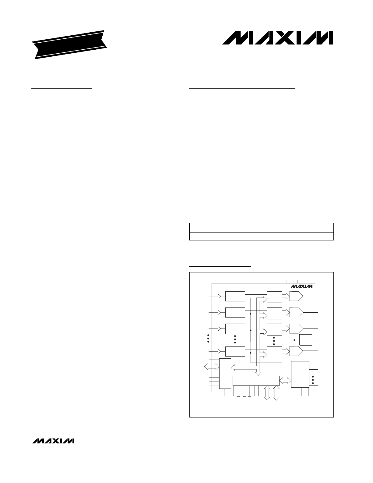
Functional Diagram
PART TEMP RANGE PIN-PACKAGE
MAX4455ECQ -40°C to +85°C 100 TQFP
4-BIT D/A
4-BIT D/A
4-BIT D/A
4 BIT D/A
V
K1
AGNDAVDDDGNDDV
MAX4455
OSD
CONTROL
AND TIMING
DAC
CURRENT
REF
OSDFILL0
OSDFILL1
OSDFILL2
RSET
OSDFILL7
OSDKEY0
OSDKEY1
OSDKEY2
OSDKEY7
XTAL1/SYNC
AD7–AD0
ADDR/DATA
VIDIN0
VIDIN1
VIDIN2
VIDIN7
RDY/BSY
DD
VIDEO TIMING
EXTRACTION
VIDEO TIMING
EXTRACTION
VIDEO TIMING
EXTRACTION
VIDEO TIMING
EXTRACTION
8
CPU
INTERFACE
RD
WR
CS
V
H1
WECASDQ RAS XTAL2
MEMORY
INTERFACE
BA
CK
11
MEMORY
ADDRESS
BUS
DIGITAL LINE
BUFFERS
DIGITAL LINE
BUFFERS
DIGITAL LINE
BUFFERS
DIGITAL LINE
BUFFERS
16
MEMORY
DATA
BUS
MAX4455
Arbitrary Graphics On-Screen Display
Video Generator
2 _______________________________________________________________________________________
ABSOLUTE MAXIMUM RATINGS
Stresses beyond those listed under “Absolute Maximum Ratings” may cause permanent damage to the device. These are stress ratings only, and functional
operation of the device at these or any other conditions beyond those indicated in the operational sections of the specifications is not implied. Exposure to
absolute maximum rating conditions for extended periods may affect device reliability.
AVDDto DVDD.............................................................-6V to +6V
AV
DD
to AGND .........................................................-0.3V to +6V
AV
DD
to DGND .........................................................-0.3V to +6V
DV
DD
to AGND.........................................................-0.3V to +6V
DV
DD
to DGND.........................................................-0.3V to +6V
V
H1
, VK1to DGND....................................................-0.3V to +6V
V
H1
, VK1to AGND ....................................................-0.3V to +6V
AGND to DGND.....................................................-0.3V to +0.3V
Analog Inputs (VIDIN_) to AGND.............-0.3V to (AV
DD
+ 0.3V)
Analog Outputs (OSDFILL_) to AGND.....-0.3V to (AV
DD
+ 0.3V)
RSET to AGND .........................................-0.3V to (AV
DD
+ 0.3V)
Memory Interface to DGND .....................-0.3V to (DV
DD
+ 0.3V)
Host Interface to DGND ..............................-0.3V to (V
H1
+ 0.3V)
OSDKEY_ to DGND.....................................-0.3V to (V
K1
+ 0.3V)
Continuous Power Dissipation (T
A
= +70°C)
100-Pin TQFP (derate 37.0mW/°C above +70°C).......2963mW
Operating Temperature Range ...........................-40°C to +85°C
Storage Temperature Range .............................-60°C to +150°C
Lead Temperature (soldering, 10s) .................................+300°C
ELECTRICAL CHARACTERISTICS
(DVDD= 3.0V to 3.6V, AVDD= 2.7V to 5.5V, V
K1
= VH1= 2.7V to 5.5V, AGND = DGND = 0, R
RSET
= 11.75kΩ±1%, R
OSDFILL_
= 75Ω,
f
XTAL1/SYNC
= 40.5MHz, TA= -40°C to +85°C, unless otherwise noted. Typical values are at TA= +25°C.) (Note 1)
PARAMETER SYMBOL CONDITIONS MIN TYP MAX UNITS
Analog Supply Voltage AV
Digital Supply Voltage DV
Host Supply Voltage V
OSDKEY Logic Supply Voltage V
Analog Supply Current AI
Digital Supply Current DI
Host Interface Static Supply
Current
Analog Power-Supply Rejection
Ratio
I
PSRR At DC 35 dB
VIDIN_ Input Resistance 100 kΩ
OSDFILL Slew Rate SR Output V
White Output Voltage Accuracy FSR Pixel data = 1111
Black Output Voltage Pixel data = 0001 ±1.5 IRE
OSDFILL DAC Linearity (Guaranteed monotonic) ±5 %FSR
Channel-to-Channel Crosstalk At 6MHz V
Key-to-Fill Timing Delay ±1 ns
RSET Pin Voltage 0.80 V
OSDKEY_ Logic Output Low V
OSDKEY_ Logic Output High V
OSDKEY_ Logic Supply Current I
DD
DD
H1
K1
All OSDFILL_ outputs at 100 IRE 190 mA
DD
f
DD
VH1
OL
OH
VK1
XTAL1/SYNC
Host interface logic levels driven to GND or
V
H1
P-P
OUT
VK1 = 5V, I
VK1 = 5V, I
SINK
SOURCE
OSDKEY_ logic levels driven to GND or V
2.7 5.5 V
3.0 3.6 V
2.7 5.5 V
2.7 5.5 V
= 40.5MHz 30 mA
10 µA
= 0.7V 140 V/µs
AVDD = 2.7V -8.2 +8.2
AV
= 5.5V -7.5 +7.5
DD
= 0.7V
P-P
60 dB
= 4mA 0.45 V
= 4mA 2.4 V
K1
10 µA
IRE
MAX4455
Arbitrary Graphics On-Screen Display
Video Generator
_______________________________________________________________________________________ 3
µP HOST INTERFACE—DC CHARACTERISTICS
(DVDD= 3.0V to 3.6V, AVDD= 2.7V to 5.5V, VK1= VH1= 2.7V to 5.5V, AGND = DGND = 0, R
RSET
= 11.75kΩ±1%, R
OSDFILL_
= 75Ω,
f
XTAL1/SYNC
= 40.5MHz, TA= -40°C to +85°C, unless otherwise noted. Typical values are at TA= +25°C.) (Note 2)
µP HOST INTERFACE—AC CHARACTERISTICS
(DVDD= 3.0V to 3.6V, AVDD= 2.7V to 5.5V, VK1= VH1= 2.7V to 5.5V, AGND = DGND = 0, R
RSET
= 11.75kΩ ±1%, R
OSDFILL_
= 75Ω,
f
XTAL1/SYNC
= 40.5MHz, C
HOST
= 50pF, TA= -40°C to +85°C, unless otherwise noted. Typical values are at TA= +25°C.) (Note 2)
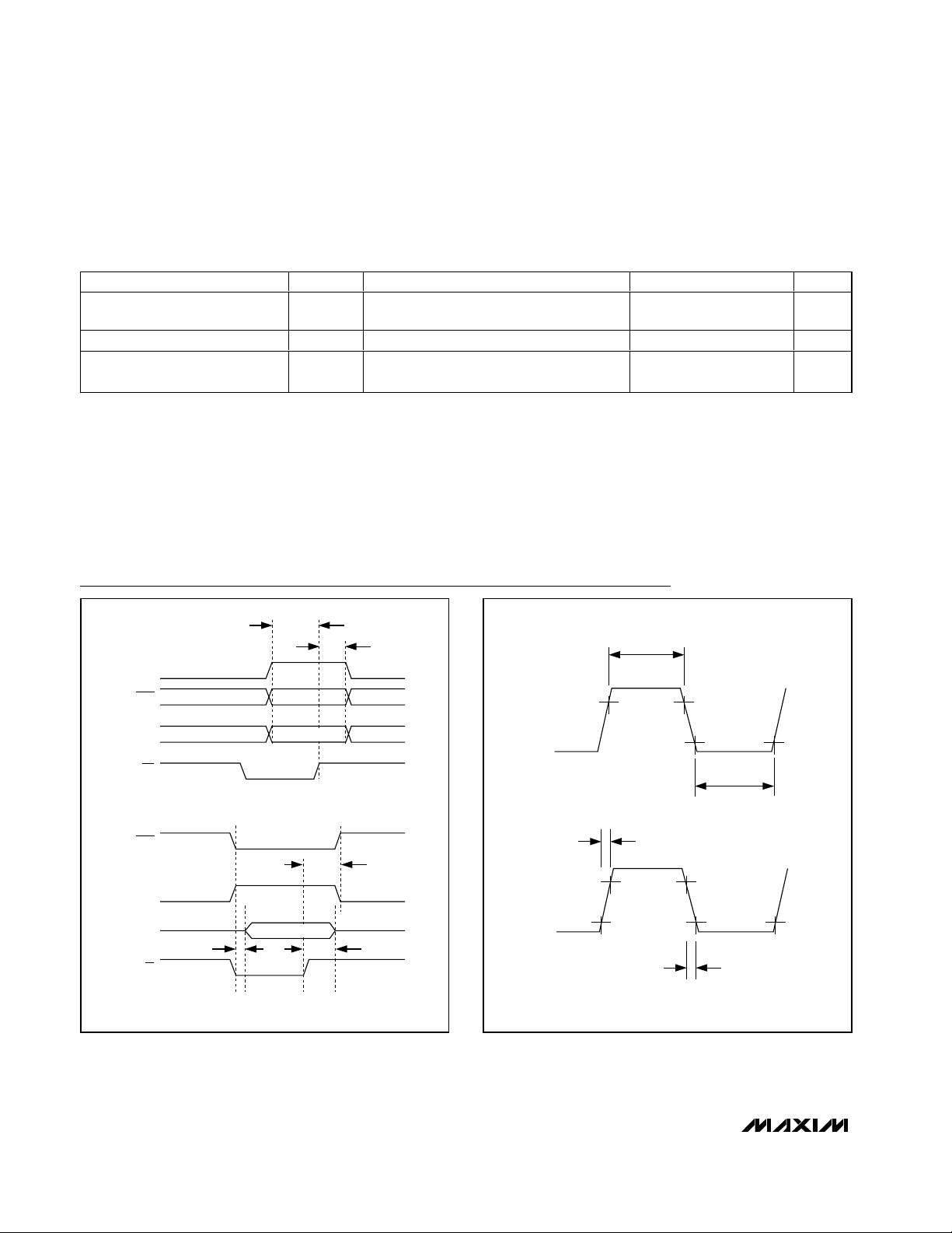
(Figure 1)
CLOCK TIMING CHARACTERISTICS
(DVDD= 3.0 to 3.6V, AVDD= 2.7V to 5.5V, VK1= VH1= 2.7V to 5.5V, AGND = DGND = 0, R
RSET
= 11.75kΩ ±1%, R
OSDFILL_
= 75Ω,
f
XTAL1/SYNC
= 40.5MHz, TA= -40°C to +85°C, unless otherwise noted. Typical values are at TA= +25°C.) (Note 4) (Figure 2)
MEMORY INTERFACE—DC CHARACTERISTICS
(DVDD= 3.0V to 3.6V, AVDD= 2.7V to 5.5V, VK1= VH1= 2.7V to 5.5V, AGND = DGND = 0, R
RSET
= 11.75kΩ ±1%, R
OSDFILL_
= 75Ω,
f
XTAL1/SYNC
= 40.5MHz, TA= -40°C to +85°C, unless otherwise noted. Typical values are at TA= +25°C.) (Note 2)
Logic Input Voltage Low V
Logic Input Voltage High V
Logic Input Current IIL / I
Logic Output Low V
Logic Output High V
PARAMETER SYMBOL CONDITIONS MIN TYP MAX UNITS
IL
IH
Sinking or sourcing 10 µA
IH
OL
OH
VH1 = 5V, I
VH1 = 5V, I
= 4mA 0.45 V
SINK
= 4mA 2.4 V
SOURCE
CS, ADD/DATA, AD7–AD0 Setup
Time Before WR Deassertion
CS Hold After WR Deassertion t
Read Data Access Time t
Read Data Out to High-Z Time t
PARAMETER SYMBOL CONDITIONS MIN TYP MAX UNITS
t
1
2
(Note 3) 50 ns
4
5
( 0.2 × V
- 0.1
( 0.2 × V
+ 1.2
)
H 1
30 ns
30 ns
15 25 ns
H 1
)
V
V
Master Clock Frequency f
Master Clock Input Low Time t
Master Clock Input High Time t
PARAMETER SYMBOL CONDITIONS MIN TYP MAX UNITS
CLKIN
CLCXtCLKIN
CHCX
Crystal oscillator or externally driven for
specified performance
t
CLKIN
= 1 / f
= 1 / f
(Note 6) 10 ns
CLKIN
(Note 6) 10 ns
CLKIN
Logic Input Voltage Low V
Logic Input Voltage High V
Logic Input Current IIL / I
Logic Output Low V
Logic Output High V
PARAMETER SYMBOL CONDITIONS MIN TYP MAX UNITS
IL
IH
Sinking or sourcing 10 µA
IH
OL
OH
DVDD = 3.3V, I
DVDD = 3.3V, I
= 4mA 0.45 V
SINK
= 0.5mA 2.4 V
SOURCE
40.5 40.6 MHz
( 0.2 × D V
- 0.1
( 0.2 × D V
+ 1.3
D D
)
)
D D
V
V
MAX4455
Arbitrary Graphics On-Screen Display
Video Generator
4 _______________________________________________________________________________________
MEMORY INTERFACE TIMING CHARACTERISTICS
(DVDD= 3.0V to 3.6V, AVDD= 2.7V to 5.5V, VK1= VH1= 2.7V to 5.5V, AGND = DGND = 0, R
RSET
= 11.75kΩ ±1%, R
OSDFILL_
= 75Ω,
f
XTAL1/SYNC
= 40.5MHz, TA= -40°C to +85°C, unless otherwise noted. Typical values are at TA= +25°C.)
Note 1: f
XTAL1/SYNC
is production tested at 1MHz. Application operating frequency is f
XTAL1/SYNC
= 40.5MHz.
Note 2: Pertains to host interface pins: ADDR/DATA, CS, WR, RD, AD7–AD0, RDY/BSY. V
H1
is connected to µP host power supply
rail (2.7V to 5.5V).
Note 3: Read operation is combinational. Access time is from the latter of either RD or CS.
Note 4: Pertains to XTAL1/SYNCIN and XTAL2 pins (external clock is supplied to XTAL1/SYNCIN pin). All input signals are specified
with t
R
= tF= 5ns (10% to 90% of DVDD), and timed from a voltage level of 1.6V.
Note 5: Specified using 10% and 90% points.
Figure 2. Clock and Memory Timing Diagram
Figure 1. µP Host Interface Timing
Timing Diagrams
Digital Output Maximum Rise
Time
Digital Output Maximum Fall Time t
Maximum Digital Out to Digital
Out Skew
PARAMETER SYMBOL CONDITIONS MIN TYP MAX UNITS
t
CLCH
CHCL
t
SKEW
15pF load (Note 5) 3 ns
15pF load (Note 5) 3 ns
15pF load, except D0–D15 ±2.5 ns
t
1
t
CHCX
V
IH
V
IL
t
CLCX
V
IH
V
IL
t
CHCL
ADD/DATA
AD7–AD0
WR
ADD/DATA
AD7–AD0
CS
HOST ADDRESS OR DATA WRITE OPERATION
CS
t
4
RD
ADDR/DATA IN
READ DATA OUT
t
2
XTAL1/SYNC
t
CLCH
t
3
MEMORY
LOGIC I/O
t
5
HOST DATA READ OPERATION
MAX4455
Arbitrary Graphics On-Screen Display
Video Generator
_______________________________________________________________________________________ 5
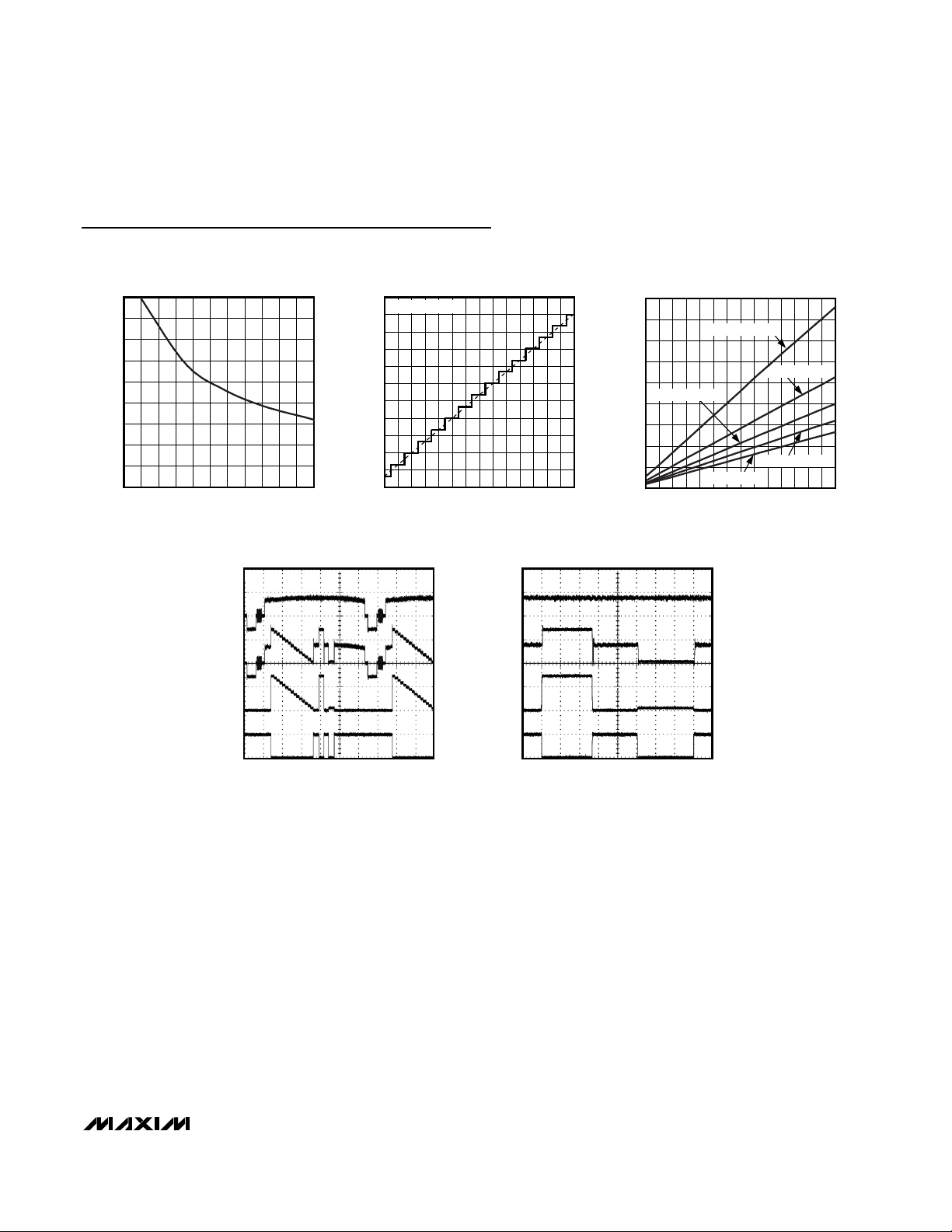
Typical Operating Characteristics
(AVDD= 5V, DVDD= 3.3V, R
RSET
= 11.75kΩ, TA= +25°C, unless otherwise noted.)
FULL-SCALE OUTPUT vs. R
225
200
175
150
125
100
75
FULL-SCALE OUTPUT (IRE)
50
25
0
415
R
(kΩ)
RSET
RSET
141311 126 7 8 9 105
VIDEO LINE OUTPUT WITH OSD
A
B
MAX4455 toc01
110
R
RSET
100
90
80
70
60
50
40
DAC OUTPUT (IRE)
30
20
10
0
115
MAX4455 toc04
DAC OUTPUT vs. DAC CODE
= 11.75kΩ
DAC CODE
0
A
0
B
DAC OUTPUT vs. DAC CODE
225
200
MAX4455 toc02
175
150
125
R
= 11.75kΩ
RSET
100
DAC OUTPUT (IRE)
75
50
25
141311 124 5 6 7 8 9 102 3
0
115
VIDEO LINE OUTPUT WITH OSD
(EXPANDED TIME SCALE)
MAX4455 toc05
R
RSET
vs. R
RSET
R
= 5.716kΩ
RSET
= 17.516kΩ
DAC CODE
0
0
R
RSET
R
RSET
MAX4455 toc03
= 7.636kΩ
= 14.598kΩ
141311 124 5 6 7 8 9 102 3
C
D
10µs/div
A: V
(NTSC COMPOSITE), 500mV/div
CAMERA
B: V
CAMERA + OSDFILL
C: V
OSDFILL
D: V
OSDKEY
NOTE: MEASUREMENT MADE WITH MAX4455EVSYS.
, 500mV/div
, 5V/div
, 500mV/div
0
0
C
D
A: V
CAMERA
B: V
CAMERA + OSDFILL
C: V
OSDFILL
, 5V/div
D: V
OSDKEY
NOTE: MEASUREMENT MADE WITH MAX4455EVSYS.
1µs/div
(NTSC COMPOSITE), 500mV/div
, 500mV/div
, 500mV/div
0
0
MAX4455
Arbitrary Graphics On-Screen Display
Video Generator
6 _______________________________________________________________________________________
Typical Operating Characteristics (continued)
(AVDD= 5V, DVDD= 3.3V, R
RSET
= 11.75kΩ, TA= +25°C, unless otherwise noted.)
Figure 3. On-Screen Display Capability of the MAX4455
MAX4455
Arbitrary Graphics On-Screen Display
Video Generator
_______________________________________________________________________________________ 7
Pin Description
PIN NAME FUNCTION
2, 1, 100, 99, 98, 97,
96, 95
3V
4, 25, 33, 42, 50, 58,
66, 72, 75
5 CS Host Chip Select Digital Input. Drive CS logic high to enable the host data interface.
6
7 RD Host Read Strobe Digital Input
8 ADDR/DATA Host Address or Data Select Digital Input
9–16 AD7–AD0 Host Address/Data Bus Digital I/O
17 RDY/BSY Host Ready/Busy Handshake Digital Output
18–23, 26, 27, 37,
36, 35, 34, 31, 30,
29, 28
24, 32, 41, 49, 57, 71 DV
38 DQM
39 CLK Memory Clock Digital Output
48 WE Memory Write Enable Digital Output
51 CAS Memory Column Address Strobe Digital Output
52 RAS Memory Row Address Strobe Digital Output
53 BA Memory Bank Address Digital Output
55, 56, 59, 60, 47,
46, 45, 44, 43, 40, 54
61–64, 67–70
VIDIN0–VIDIN7
DGND Digital Ground
D0–D15 Memory Data Digital I/O
A0–A10 Memory Address Digital Outputs
OSDKEY0–
OSDKEY7
Analog Video Inputs. The MAX4455 extracts video timing information from each VIDIN_
input. AC-couple the input signal with a 0.1µF capacitor.
H1
WR Host Write Strobe Digital Input
DD
Host Interface Supply Voltage Input. VH1 supplies the level shifters for logic outputs to the
host µP interface. Connect V
Positive Digital Power Supply. Bypass each DVDD pin with a 0.1µF capacitor to DGND.
Memory DQM Digital Output. DQM controls the memory output buffer in read mode, and
masks input data in write mode.
OSDKEY Digital Outputs. OSDKEY_ logic low controls the fast mux switches (available in
the Maxim crosspoint switches, MAX4356/MAX4358) to insert OSDFILL_ signal.
to the µP logic supply.
H1
65 V
73 XTAL1/SYNC
74 XTAL2
76, 78, 80, 82, 84,
86, 88, 90, 92
77, 79, 81, 83, 85,
87, 89, 91
K1
AV
DD
OSDFILL7–
OSDFILL0
OSDKEY Interface Power-Supply Input. VK1 supplies the level shifters for OSDKEY_ logic
outputs to the fast mux switches (available in the Maxim crosspoint switches,
MAX4356/MAX4358). Connect V
the MAX4356/MAX4358).
Crystal Oscillator/External Clock Input. Connect a crystal oscillator module to
XTAL1/SYNC, or connect a fundamental mode crystal oscillator between XTAL1/SYNC and
XTAL2.
Crystal Oscillator Output. Leave XTAL2 unconnected when using a crystal oscillator
module, or connect a fundamental mode crystal oscillator between XTAL1/SYNC and
XTAL2.
Positive Analog Power Supply. Bypass each AVDD pin with a 0.1µF capacitor to AGND.
OSDFILL Analog Outputs. OSDFILL_ are video DAC current outputs and require a
termination resistor (nominally 75Ω) to AGND.
to the digital supply of the fast mux switches (VDD of
K1
MAX4455
Arbitrary Graphics On-Screen Display
Video Generator
8 _______________________________________________________________________________________
Detailed Description
The MAX4455 provides 4-bit gray-scale graphics video
to eight simultaneous independent composite video
inputs. The bit-mapped approach allows an arbitrary
message to be inserted into the camera video when
used in conjunction with the MAX4356/MAX4358 video
crosspoint switch or discrete fast mux switch. The
inserted graphics can include camera location, date,
time, company logo, or warning prompts.
The graphics palette for each of the eight video channels
in the MAX4455 is logically organized into 1024 pixels by
512 lines. This memory arrangement facilitates easy
row/column pixel addressing by the host processor. The
actual displayed area is 712 × 484 NTSC (712 × 512 PAL)
pixels. The remaining 312 logical pixels per line are
blanked. The remaining 28 NTSC (0 PAL) horizontal lines
are also blanked as shown in Figure 4.
The MAX4455 controls a 16Mb SDRAM (such as
MT48LC1M16A) that stores video graphics insertion data.
The MAX4455 performs all SDRAM support functions,
including refresh, RAS/CAS timing, video addressing, and
CPU access cycles for host processor read/write support.
Since the SDRAM is organized as a 16-bit wide × 1 million deep array, each SDRAM memory location holds 4
pixels (based on the fact that a pixel is 4 bits and memory is 16 bits wide). The host processor thus accesses
pixels four at a time. The host processor interface is 8
bits wide so the 16 bit wide SDRAM data is written into
(or read from) the pixel data register as two separate
8-bit bytes.
The MAX4455 establishes a video raster time base by
sensing the video signal on either the output of the
Maxim crosspoint switch, or the output buffer of the fast
mux switch. The MAX4455 uses this raster timing to
produce an OSD image signal that can be inserted into
the camera video by controlling the OSDKEY input to
the Maxim crosspoint switch or fast mux switch. The
OSD image is inserted wherever the OSD video level
pixel code has a nonzero value, and the crosspoint
switch or discrete fast mux is made to pass the original
video wherever the OSD video level pixel code is zero.
When the OSD video level is nonzero, it represents a
gray-level code such that level 1 is near black and
code 15 (the maximum possible with a 4-bits-per-pixel
code) is maximally white (Table 1). The host computer
fills the external OSD frame memory with a bit-mapped
image such that each pixel has a value between zero
and 15, controlling both insertion locations and the
brightness levels within an inserted video image. There
are eight channels in the MAX4455 that share memory
resources but are logically completely independent.
Writing/reading image data to/from any channel’s memory does not disrupt other channels.
The MAX4455 features a memory-sharing function
where the even channels or the odd channels can be
updated simultaneously by writing to a designated
source channel. The memory-sharing function minimizes the number of memory writes by the host processor. This is useful for updating information that changes
rapidly (i.e., time stamp).
Video Inputs
The MAX4455’s eight VIDIN_ inputs include circuitry to
extract video timing from each asynchronous video
channel for proper display of the OSD specific to that
channel. Each VIDIN_ time-base circuitry includes a
horizontal sync detector, vertical sync detector, vertical
interval detector, horizontal line counter, and even/odd
field counter. The VIDIN_ inputs sense a standard 1V
P-P
video signal at the output of the crosspoint switch, or
fast mux buffer in order to make video timing insensitive
to delays through the switch/mux. AC-couple the input
with a 0.1µF capacitor.
OSDFILL_ Video Outputs
The MAX4455 has eight independent current output
video DACs that provide 7 IRE to 100 IRE video levels
(R
RSET
= 11.75kΩ) when terminated with 75Ω to
AGND. Connect OSDFILL_ to either the OSDFILL_
input of the Maxim crosspoint switch (MAX4356/
MAX4358) or to one of the inputs of the fast mux switch.
OSDKEY Control Outputs
Each OSD channel has an OSDKEY_ logic output that
drives low when OSDFILL_ output video is to be multiplexed into the active video. The OSDKEY_ output
interfaces directly to the OSDKEY_ inputs of the
MAX4356/MAX4358 or control inputs of the fast mux
switch to allow pixel-by-pixel OSD insertion. The V
K1
supply sets the OSDKEY_ logic output voltage levels.
Pin Description (continued)
PIN NAME FUNCTION
93 RSET
94 AGND Analog Ground
OSDFILL Reference Voltage. Connect a resistor (typically 11.75kΩ) from RSET to AGND to
set the full-scale output current of all eight OSDFILL_ outputs.
MAX4455
Arbitrary Graphics On-Screen Display
Video Generator
_______________________________________________________________________________________ 9
Connect VK1to the MAX4356/MAX4358 VDDlogic supply, or a 5V logic supply for TTL output compatibility.
OSDFILL_ Reference Voltage (RSET)
Set the video DAC’s full-scale output current for all
eight channels by connecting a resistor between RSET
and ground. The nominal 11.75kΩ R
RSET
provides a
100 IRE video output level when OSDFILL_ outputs are
terminated with 75Ω resistors to ground. R
RSET
can typ-
ically range between 5kΩ and 15kΩ.
The full-scale OSD DAC output current = (106.5) / R
RSET
.
The full-scale OSD DAC output voltage is the OSD DAC
output current × R
OSDFILL
, where ROSDFILL_ is the termi-
nation resistor to AGND at OSDFILL_.
Crystal Oscillator
The MAX4455 requires a 40.5MHz clock. Connect a 3.3V
crystal oscillator module to XTAL1/SYNC and leave
XTAL2 unconnected, or connect a lower cost 40.5MHz
fundamental mode crystal between XTAL1/SYNC and
XTAL2. The MAX4455 is designed to operate with a 50%
clock duty cycle, but typically operates with up to 40% to
60% duty cycles. The oscillator circuitry typically requires
10ms to settle after the DV
DD
supply is powered up.
Microprocessor Interface
The MAX4455 µP interface includes a byte-wide
address/data bus (AD7–AD0) for parallel programming
of the MAX4455, write strobe input (WR), read strobe
input (RD), active-high chip-select input (CS), address
or data-select input (ADDR/DATA), and a ready/busy
hand-shaking output (RDY/BSY) (Figures 5 and 6). The
MAX4455 allows for interfacing to a µP powered from a
different supply than the MAX4455 by connecting V
H1
to the µP supply. For example, the MAX4455 can be
operated with a single 3.3V supply, while the µP interface can be operated with 3.3V or 5V logic levels by
connecting VH1to the µP power supply.
Host Access Protocol Sequence
1) Host sets ADD/DATA = 1.
2) Host outputs register address on AD7–AD0.
3) Host pulses WR low, then high to write register
address.
4) Host checks RDY/BSY = 1 (host waits if RDY/BSY = 0).
For register data writes:
1) Host sets ADD/DATA = 0.
2) Host drives register data on AD7–AD0.
3) Host pulses WR low, then high.
For register data reads:
1) Host removes drive from AD7–AD0 in anticipation of
register read operation and sets ADD/DATA = 0.
2) Host then pulses RD low and reads register data.
3) The MAX4455 three states when RD is deasserted
(high).
SDRAM Memory Interface
The MAX4455 interfaces directly to a 16Mb SDRAM
with 16-bit-wide data bus. The MAX4455 performs all
SDRAM support functions, including refresh, RAS/CAS
timing, data addressing, and CPU access cycles for
host processor read/write support.
MAX4455 Register Description
OSD Register Organization
The host processor controls each of the MAX4455’s
eight video channels through eight groups (blocks) of 8bit command, status, data, and address registers, plus
one multichannel register block. The register set description for a single channel is described in Table 2. The
eight identical sets of 16 registers (14, plus 2 reserved)
are selected by 4 LSB bits in the host interface address
field as described in Tables 3 and 4. The lower address
bits select which register is accessed within any given
channel. Even channels can share buffer data for display
Table 1. Pixel Data Mapping (4 Bits per
Pixel)
PIXEL DATA GRAY SCALE DESCRIPTION
Transparent—no OSD
0000 0
0001 1 7 IRE (black)
0010 2 13 IRE
0011 3 20 IRE
0100 4 27 IRE
0101 5 33 IRE
0110 6 40 IRE
0111 7 47 IRE
1000 8 53 IRE
1001 9 60 IRE
1010 10 67 IRE
1011 11 73 IRE
1100 12 80 IRE
1101 13 87 IRE
1110 14 93 IRE
1111 15 100 IRE (white)
insertion. Background
video appears normally.

MAX4455
Arbitrary Graphics On-Screen Display
Video Generator
10 ______________________________________________________________________________________
among even channels. Odd channels can also share
buffer data for display among odd channels (see the
Memory Sharing section).
Detailed Description of the Channel-N
Block Registers
QPH, QPL (Quad Pixel Register)
Read/write pixel data 16-bits at a time to the quad pixel
registers due to the SDRAM memory organization. The 4
MSBs (nybble) of QPH represent the left-most pixel and
the 4 LSBs of QPL represent the right-most pixel (4 bits
per pixel). To transfer the QPH/QPL value into display
memory, set the QPHORIZ/QPLINE registers and then
write 0000 0010 to the command register (see Command
Register section).
QPHORIZ
This 8-bit value is the address of the quad pixel within
the line specified by QPLINE HI and QPLINE LO. A
zero in QPHORIZ addresses the leftmost displayed
quad pixel in the specified line, and increasing
QPHORIZ addresses indexes towards the right-hand
side of the video screen. Valid values range from zero
to 177. Write a 1 in the HINC bit of the channel status
register to enable autoincrement of QPHORIZ.
QPHORIZ autoincrement saturates at 177.
QPLINEH, QPLINEL
The QPLINE_ 9-bit address specifies the horizontal line
of the quad pixel to be accessed (host read or write).
The 9th bit resides in the LSB position (bit 0) of the
QPLINEH register. The lower 8 bits of the 9-bit address
are specified by QPLINEL. Table 5 shows valid displayed line numbers. Note that for NTSC, lines 1
through 20 are never valid, as this is the vertical blank
interval. Write a 1 in the VINC bit of the channel status
register to enable autoincrement of QPLINE_. QPLINE_
autoincrement saturates at 511.
Figure 4. OSD Raster Dimensions
Figure 5. µP Host Interface
t
= 33.367ms
T = 1 / (13.5MHz) = 74.074ns = 1 PIXEL TIME
FRAME
VERTICAL 1 (20 NTSC LINES, 25 PAL LINES)
FLD1: 262H/
312H (PAL)
HBLANK
525H / 625H PER FRAME
FLD2: 263H/
313H (PAL)
HBLANK
APPROX
144T NTSC,
162T PAL
HBLANK PIXEL COUNT IS DEPENDENT
UPON INCOMING VIDEO HLINE PERIOD
FIELD 1 ACTIVE VIDEO (242H NTSC, 287H PAL)
VERTICAL 2 (21 NTSC LINES, 26 PAL LINES)
FIELD 2 ACTIVE VIDEO (242H NTSC, 287 PAL)
712T NTSC,
702T PAL
1ST DISPLAYED PIXEL POSITION IS CONTROLLED
BY HOFFSET REGISTER
µP DIGITAL SUPPLY
2.7V TO 5.5V
V
CC
µP
DATA BUS
GPIO
MAX4455 DIGITAL SUPPLY
3V TO 3.6V
V
H1
WR
RD
ADD/DATA
8
AD7–AD0
RDY/BSY
CS
DV
DD
µP HOST INTERFACE
MAX4455

MAX4455
Arbitrary Graphics On-Screen Display
Video Generator
______________________________________________________________________________________ 11
STATUS
The channel status register contains a group of individual control bits and a loss-of-sync (LOS) flag bit. BLANK
(when set to 1) forces suppression of the OSD insertion
graphics, independent of the memory contents. ASYNC
(when set to 1) enables the SHRxxxx registers to be
updated by the host immediately; otherwise, they are
updated at the next complete video field. HINC (when
set to 1) enables autoincrement of the QPHORIZ regis-
ter after each host read/write to OSD memory. VINC
(when set to 1) enables autoincrement of QPLINEH/L
after each host read/write to OSD memory. The LOS flag
is useful in detecting the presence (or absence) of composite video at the channel VIDIN_. LOS is a 1 if the
channel’s valid composite sync is lost for more than one
horizontal line period. It resets back to zero once a valid
sync pulse is detected.
Figure 6. Host Data Write and Read Sequences
The channel status register is described below:
BIT7 BIT0
0 0 0 VINC HINC ASYNC BLANK LOS
CS
ADD/DATA
AD7–AD0
HIGH-Z
ADDRESS
DATA IN
WR
RD
CS
ADD/DATA
AD7–AD0
WR
RD
HOST ADDRESS AND DATA WRITE OPERATION
HIGH-Z
ADDRESS
HOST ADDRESS AND DATA READ OPERATION
DATA OUT

MAX4455
Arbitrary Graphics On-Screen Display
Video Generator
12 ______________________________________________________________________________________
Table 2. Channel-N Block Register Map
Table 3. Channel Block Addressing
Note: nnn = 000 to 111 for channels 0 to 7, respectively.
ADDRESS NAME DESCRIPTION
0nnn0000 QPH Quad pixel high data read/write. Most significant nybble = leftmost pixel.
0nnn0001 QPL Quad pixel low data read/write. Least significant nybble = rightmost pixel.
0nnn0010 QPHORIZ Quad pixel within H line address
0nnn0011 QPLINEH Quad pixel line address high
0nnn0100 QPLINEL Quad pixel line address low
0nnn0101 STATUS Loss of sync for channel N, control bits
0nnn0110 COMMAND Command register
0nnn0111 HOFFSET Horizontal offset
0nnn1000 VOFFSET Vertical offset
0nnn1001 SHRSRC Shared buffer source channel (0, 2, 4, 6) for even channels, (1, 3, 5, 7) for odd channels
0nnn1010 SHRBEGH Shared buffer beginning line high
0nnn1011 SHRBEGL Shared buffer beginning line low
0nnn1100 SHRENDH Shared buffer end line high
0nnn1101 SHRENDL Shared buffer end line low
0nnn1110 Reserved Reserved
0nnn1111 Reserved Reserved
ADDRESS CHANNEL
0000xxxx 0
0001xxxx 1
0010xxxx 2
0011xxxx 3
0100xxxx 4
0101xxxx 5
0110xxxx 6
0111xxxx 7
1000xxxx Multichannel
1001xxxx to 1111xxxx Reserved addresses

MAX4455
Arbitrary Graphics On-Screen Display
Video Generator
______________________________________________________________________________________ 13
COMMAND
The channel command register allows writing and reading of quad pixel data into external SDRAM memory.
The read and write operations are described below:
• Writing 0000 0010 to the COMMAND register caus-
es the pixel data in QPH and QPL to be stored into
external SDRAM memory.
• Writing 0000 0001 to the COMMAND register copies
from external SDRAM memory the quad pixels specified by QPHORIZ/QPLINE into QPH/QPL.
• Writing 0000 0011 to COMMAND register causes a
write followed by a readback to verify the data.
Table 4. Multichannel Block Register Map (Common to All Eight Channels)
Table 5. QPLINE Mapping
The command register is described below:
HOFFSET
The channel horizontal offset register defaults at powerup to 128. Values less than 128 shift the OSD image to
the left (as viewed on the display), while values greater
than 128 shift the OSD image to the right. For example,
changing HOFFSET from 128 to 110 shifts the image to
the left by approximately 10% of the visible display.
Changing HOFFSET from 128 to 156 shifts the image to
the right by approximately 10% of the visible display.
The image portion shifted beyond the active video is
automatically blanked on any edge. The units of HOFFSET are in quad pixels. Horizontal offset is used to
allow flexibility in the video timing for various video
sources. Horizontal offset ensures that the first logical
OSD pixel is visible on the left-hand edge of the video
monitor screen.
ADDRESS NAME DESCRIPTION
10000000 QPH Quad pixel high data read/write for multiple write
10000001 QPL Quad pixel low data read/write for multiple write
10000010 QPHORIZ Quad pixel within H line address
10000011 QPLINEH Quad pixel line address high
10000100 QPLINEL Quad pixel line address low
10000101 LOSALL Loss-of-sync flags for channels 0 through 7
10000110 MWRITE Command register, triggers multiple write(s)
10000111 CONTROL Control bits
10001000 TO 10001111 Reserved Reserved registers
QPLINE
0 0000 0000
0 0000 0001
0 0000 0010
0 0000 0011
0 1111 1110
0 1111 1111
1 1111 0010 Field 2, line 263 —
1 1111 1111 — Field 2, line 276
NTSC (VOFFSET = 128)
FIELD, LINE
Field 1, line 21
Field 2, line 21
Field 1, line 22
Field 2, line 22
Field 1, line 148
Field 2, line 148
PAL (VOFFSET = 133)
FIELD, LINE
Field 1, line 26
Field 2, line 26
Field 1, line 27
Field 2, line 27
Field 1, line 153
Field 2, line 153
BIT7 BIT0
000000WRITE READ

MAX4455
Arbitrary Graphics On-Screen Display
Video Generator
14 ______________________________________________________________________________________
SHRBEGH, SHRBEGL
Share begin line HI, share begin line LO. This register
pair contains a 9-bit address, which specifies the starting horizontal line to be used from the shared video
frame buffer memory. SHRBEG HI contains only 1 bit,
which resides in the LSB position (bit 0) of the SHRBEG
HI register. The lower 8 bits of the 9-bit address are
specified by SHRBEG LO. Valid shared line numbers
range from 0 to 483 NTSC (511 PAL). The ASYNC flag
in the channel status register controls the time of actual
update, either immediate (asynchronous) or video field
synchronous. SHRBEGH contains the upper bits of the
starting line address and SHRBEGL contains the lower
bits of the line starting address. To allow the entire
value to be changed at once, the internal value of
SHRBEG (which uses both SHRBEGH and SHRBEGL)
is not updated until SHRBEGL is written. A write to
SHRBEGH alone does not trigger an update of the
internal SHRBEG value.
SHRENDH, SHRENDL
This register pair, share end line HI, share end line LO,
contains a 9-bit address, which specifies the ending
horizontal line to be used from the shared video frame
buffer memory. SHREND HI contains only 1 bit, which
resides in the LSB position (bit 0) of the SHREND HI
register. The lower 8 bits of the 9-bit address are specified by SHREND LO. Valid shared line numbers range
from 0 to 483 visible NTSC (511 PAL). The ASYNC flag
in the channel status register controls the time of actual
update, either immediate (asynchronous) or video field
synchronous. To allow the entire value to be changed
at once, the internal value of SHREND (which uses both
SHRENDH and SHRENDL) is not updated until
SHRENDL is written. A write to SHRENDH alone does
not trigger an update of the internal SHREND value.
The shared memory source channel register is described below:
VOFFSET
The channel vertical offset register defaults at power-up
to 128. Values less than 128 shift the image up while
values greater than 128 shift the OSD image down. For
example, changing VOFFSET from 128 to 80 shifts the
image up by approximately 10% of the visible display.
Changing VOFFSET from 128 to 176 shifts the image
down by approximately 10% of the visible display. This
register controls the vertical offset of the OSD graphics
insertion video. The units of VOFFSET are logical lines.
Vertical offset ensures that the first logical OSD graphics line is visible on the video monitor screen. Updates
to VOFFSET can take up to two full frame periods to
take effect.
SHRSRC
Shared memory source channel. A nonzero value in
SHRSRC replaces a horizontal band of display with data
from another channel. When an SHRSRC channel is
selected (nonzero value in the SHRSRC register), the
channel’s graphics video is generated from the channel’s memory, except for the horizontal video lines
between (and including) SHRBEGH/L and SHRENDH/L,
which instead comes from the memory channel specified by the SHRSRC register (see Applications
Information for more details on how video memory sharing works). Time of actual update, either immediate
(asynchronous) or field synchronous, is controlled by the
ASYNC flag in the channel command register. Even
channels can only be shared with even channels. Odd
channels can only be shared with odd channels.
Note: If multiple even or odd channels are set to 1, data
is taken from the lowest even channel and shared with
the higher even channels. This is also true for the odd
channels.
BIT7 BIT0
Ch7 Ch6 Ch5 Ch4 Ch3 Ch2 Ch1 Ch0

MAX4455
Arbitrary Graphics On-Screen Display
Video Generator
______________________________________________________________________________________ 15
LOSALL
This register is common to all eight channels and
reflects the status of sync presence on each of the
eight VIDIN_ inputs. If valid composite sync is present
at each of the eight VIDIN_ inputs, this register contains
all zeros. If any channel loses sync for more than one
horizontal line period, a flag is set for that respective
channel indicating sync loss. Normally, the host
processor polls this register periodically and checks for
nonzero flag bits, indicating loss of video on any or all
channels. This feature detects vandalism, security
threats, or simple camera/link failure. The loss of sync
register is described below:
MWRITE
Multiple write command register. Trigger multiple write
operations to OSD frame buffer memory by writing to
MWRITE, specifying which channels should receive
data. This is useful in updating graphics common to
multiple channels (i.e., time of day, etc.). Writing a 1
triggers writes to the desired channel as defined below.
This register autoclears itself after a multiple write cycle
completes. The multiple write register is described
below:
Control
Control bits for the multichannel block register. VINC,
when set to 1, enables autoincrement of QPLINEH/L in
the multichannel block after each host multichannel
write to OSD memory. HINC, when set to 1, enables
autoincrement of QPHORIZ in the multichannel block
after each host multichannel write operation to OSD
buffer memory. The control register is described below:
Detailed Description of the Multichannel
Block Registers
QPH, QPL
Pixel data is read/written 16 bits at a time to the quad
pixel registers due to the SDRAM memory organization.
The most significant 4 bits (nybble) of QPH represents
the leftmost pixel and the least significant 4 bits of QPL
represents the rightmost pixel (4 bits per pixel). Table 1
shows pixel data mapping. QPH and QPL for the multichannel block is read/written the same as the individual
channel-N register function, except multichannel pixel
data is used for multiple write operations to selected
channels.
QPHORIZ
This 8-bit value is the address of the quad pixel within
the line specified by QPLINE HI and QPLINE LO. A
zero value in QPHORIZ addresses the leftmost displayed quad pixel in the specified line and increasing
QPHORIZ addresses indexes towards the right-hand
side of the video screen. This register addresses multichannel write operations. Valid values range from zero
to 177. Write a 1 in the HINC bit of the multichannel
CONTROL register to enable autoincrement of
QPHORIZ. QPHORIZ autoincrement saturates at 177.
QPLINEH, QPLINEL
This 9-bit address specifies the horizontal line of the
quad pixel to be accessed (host read or write). QPLINE
HI is only 1 bit that resides in the LSB (bit 0) of the
QPLINE HI register. The lower 8 bits of the 9-bit
address are specified by QPLINE LO. Valid displayed
line numbers range from 0 to 483 NTSC (511 PAL). This
register is used for addressing for multichannel write
operations. Write a 1 in the VINC bit of the channel
CONTROL register to enable autoincrement of
QPLINE_. QPLINE_ autoincrement saturates at 511.
BIT7 BIT0
Ch7 Ch6 Ch5 Ch4 Ch3 Ch2 Ch1 Ch0
BIT7 BIT0
Ch7 Ch6 Ch5 Ch4 Ch3 Ch2 Ch1 Ch0
BIT7 BIT0
0 0 0 VINC HINC 0 0 0

MAX4455
Arbitrary Graphics On-Screen Display
Video Generator
16 ______________________________________________________________________________________
Applications Information
Interfacing to Maxim Video Crosspoint
Switches
The MAX4455 interfaces directly to MAX4356/MAX4358
video crosspoint switches with OSD insertion function
(Figure 7). The MAX4455 OSDKEY_ and OSDFILL_ outputs connect directly to the OSDKEY_ and OSDFILL_
inputs on the MAX4356/MAX4358 and utilize the internal fast mux in the MAX4356/MAX4358 to implement
the OSD insertion. To ensure correct video timing, the
MAX4455 VIDIN_ input senses and extracts the video
timing directly from the crosspoint switch output.
Interfacing the MAX4455 with a Fast Mux
Switch
The MAX4455 interfaces directly to a fast mux switch, as
shown in Figure 8. Choose a device with a switch time of
less than 30ns, such as the MAX4258, for accurate OSD
insertion. The MAX4258 is a single-channel wideband
video amplifier with input multiplexing and a channel-tochannel switching time of 20ns. Configure the amplifier
using external resistors for a 6dB gain to drive a 75Ω
back-terminated video line. Connect the OSDFILL_ output
of the MAX4455 to IN0 of the MAX4258 and connect the
video source (camera output) to IN1. Connect the
OSDKEY_ output of the MAX4455 to A0, the channel
select input of the MAX4258. When the OSDKEY_ signal
is low, the OSDFILL_ analog signal on channel IN0 passes through the mux and the OSD information is inserted
into the video image. When the OSDKEY_ signal is high,
the camera video output passes through the mux and is
displayed on the monitor.
Channel Blanking During Video Input
Source Switching
Before switching input video sources on a channel with
active OSD, set the BLANK bit to 1 in the channel status register to prevent OSDKEY assertion during the
video blanking interval. Failure to blank the OSD prior
to switching input video sources can cause OSD information to be inserted over the new video input’s vertical
blanking interval, resulting in a loss of sync on that
channel. The MAX4455 timing synchronizes to the
video output of the channel, such that switching another asynchronous input video source can cause writing
of OSD information over the new video source with
unpredictable results (i.e., OSD insertion over the vertical blanking interval).
The channel blanking procedure follows:
1) Set BLANK = 1.
2) Switch camera/video source input.
3) Set BLANK = 0.
Figure 7. Interfacing MAX4455 with MAX4358 Video Crosspoint Switch
*OPTIONAL COMPONENTS. USED TO ATTENUATE THE COLOR BURST SIGNAL
OF COLOR CAMERAS TO AVOID FALSE TRIGGERING OF THE SYNC DETECTOR
IN THE MAX4455.
MAX4455 OSD CHANNEL-N
PORTION OF
MEMORY
ALLOCATED
TO CHANNEL
MICRO-
CONTROLLER
MEMORY
INTERFACE
CPU
INTERFACE
V
K1
DIGITAL
BUFFERS
LINE
V
DD
430Ω*
0.1µF
VIDIN_
VIDEO TIMING
EXTRACTION
AND CONTROL
470pF*
CAMERA
OSDKEY_
4-BIT D/A
75Ω
OSDFILL_
V
SWITCH
MATRIX
(FAST MUX)
DD
MAX4358
VIDEO
CROSSPOINT
SWITCH
CAMERA
+OSD

MAX4455
Arbitrary Graphics On-Screen Display
Video Generator
______________________________________________________________________________________ 17
The result of writing OSD over the vertical blanking
interval is a rolling picture that the display monitor cannot sync to, and the MAX4455 loss-of-sync flag is set
for that channel. Reestablish sync by blanking the
channel’s OSD for at least one full video frame period,
allowing the MAX4455’s sync timing circuitry to correctly sense the new video source’s timing, and reset the
LOS flag.
Optimizing OSDFILL Load Termination
and R
RSET
The MAX4455 provides standard 100 IRE (0.714V) fullscale OSDFILL_ output levels with R
RSET
= 11.75kΩ and
OSDFILL_ terminated with R
OSDFILL_
= 75Ω to AGND.
The MAX4455 OSDFILL_ outputs can drive as high as
1.5V by selecting a lower R
RSET
value, or increasing the
value of R
OSDFILL
, or a combination of both. OSDFILL
output levels higher than 0.714V can have increased distortion and degraded linearity (see the OSDFILL_
Reference Voltage (RSET) section).
SDRAM Memory Selection
The MAX4455 EV kit uses the Micron MT48LC1M16TG7S SDRAM. The MAX4455 has not been tested with, but
is designed to operate with the following SDRAMS:
Micron MT48LC1M16A1-8 or faster, VIS VG3617161DT-8
or faster, Hyundai HY57V161610D or HY57V161610C,
Mitsubishi M2V64S40DTP, Micron MT48LC4M16A2, and
Hitachi HM5264165F.
Anti-Aliasing and Flicker
The MAX4455 is a high-resolution graphics system
capable of accurately displaying a single pixel line. A
line with the height of one pixel, by definition, occurs
only on one of the two interlaced fields that make up the
standard interlaced video signal. Since the interlaced
system has a frame rate of about 60Hz, the field rate is
half of this (30Hz). Any object occurring only on one
field is displayed at a 30Hz rate, resulting in a flickering
image. Any signal displayed at less than a 50Hz rate is
perceived to visibly flicker. The slower the display rate
is, the higher the perceived flicker.
The amount of flicker in a one-pixel-high horizontal line
is dependent on the length of the line. The flicker associated with very short lines that are part of another
shape are typically very minimal. For example, the flicker of the legs of the letter F is almost imperceptible. At
the other extreme, a one-pixel horizontal line that spans
the width of a display exhibits flicker that can be very
noticeable.
The perceived flicker due to thin horizontal lines can be
minimized by making the line thicker or by using antialiasing techniques. For the best results, these two
Figure 8. Interfacing MAX4455 with a Fast Mux Switch
FB
OSDFILL_
(FROM MAX4455)
+1
IN0
CAMERA
SWITCH
MATRIX
OUT1
IN1
(FROM MAX4455)
AO
OSDKEY_
510Ω510Ω
+5V
TO MAX4455
VIDIN_ INPUT
+1
75Ω
MAX4258
-5V

MAX4455
Arbitrary Graphics On-Screen Display
Video Generator
18 ______________________________________________________________________________________
techniques can be used in conjunction. A thicker line
exhibits much less of the flicker effect. Once the line is
from five to six lines thick, the additional improvement
from thicker lines is negligible.
Anti-aliasing is a fairly well-known technique that involves
decreasing the severity of the transition of the graphic or
font structure. Here, it involves bracketing a horizontal line
with two or more other lines that have a relative brightness that is between the brightness level of the line and
the background. This is illustrated in Figure 9.
The proper application of this technique softens the
look of the line, which can be undesirable in some
cases. In general, it makes the display easier to read.
Finite Switch Time Effects
The MAX4455 generates the OSDFILL_ and OSDKEY_
signals time coincident with each other within a few
nanoseconds. Since the OSDKEY_ signal controls
when the external fast mux switch switches from normal
camera video to the OSDFILL signal, any finite delay in
the response time of this fast mux switch has an effect
on the resulting OSD insertion (Figure 10).
Due to the finite switching time of the fast mux switch,
both the leading and trailing portions of the OSDFILL_
are inserted slightly later in time. The leading edge
does not create a visible artifact on the screen since it
only shifts the image to the right an amount equal to the
switch delay. The trailing edge of the OSDFILL_ can
result in a visible artifact because the OSDFILL_ signal
has already returned to 0 IRE before the fast mux
switch can transition back to the camera video signal.
This effect is shown in Figure 11.
In a typical NTSC system with a bandwidth of 4.2MHz,
the narrowest resolved image is about 120ns wide. If the
delay of the fast mux switch is less than half of this, 60ns
or less, no visible artifact should be seen on the display.
The displayed information can be designed to dramatically minimize the adverse effect of the finite switch time,
if desired. For example, virtually all fonts and graphics
that are overlayed on normal video need to be outlined
for good readability. A very common technique is to use
white structures with a black outline border. To compensate for the above finite switch time effect, construct the
graphic or font with a thinner trailing edge. When displayed, it looks symmetrical with the trailing edge appearing normal. Figure 12 illustrates this technique.
Memory Sharing
Memory sharing is a feature that reduces the host
processor burden for tasks such as time-stamp update.
The MAX4455 supports user-specified starting and
ending lines to be shared by any number of channels.
In Figure 13, the time stamp is written only to channel 0
on line start through line end. Graphics data stored in
lines outside of start and end remain unique for each of
the eight video channels (Figure 13).
In Figure 13, channel 0’s start line number through end
line number are duplicated onto channel 2 and channel
4’s display. The source of shared data is defined in the
SHRSHC register (see the MAX4455 Registed Descrip-
tion section). For example, channel 15 can be programmed to display channel 7’s graphics beginning at
channel 7 start line #n through end line #m, etc.
Sharing is restricted to even channels with even channels and odd channels with odd channels. For example, channels 1, 3, 5, 7 can share lines and channels 0,
2, 4, 6 can share lines in any combination.
Power Supplies and Bypassing
The MAX4455 operates from a single 2.7V to 5.5V analog
supply and a 3V to 3.6V digital supply. Additional logic
supplies for host µP interface (VH1) and the OSDKEY_
interface (VK1) allow the MAX4455 to interface with other
logic supplies from 2.7V to 5.5V. Bypass each supply pin
with a 0.1µF capacitor to ground.
Layout Concerns
For best performance, make the OSDFILL_ and OSDKEY_ output traces as short as possible, and place the
75Ω termination resistor close to the crosspoint switch
OSDFILL_ input with the resistor terminated to the solid
analog ground plane. The SDRAM interface is the highest speed connection and therefore requires careful
layout. Place the SDRAM close to the MAX4455 to minimize trace lengths. The MAX4455 pinout is optimized
for memory bus trace routing to the SDRAM without
crossing traces. Refer to the MAX4455 EV kit for a
proven PC board layout.

MAX4455
Arbitrary Graphics On-Screen Display
Video Generator
______________________________________________________________________________________ 19
Figure 9. Anti-Aliased Line Drawing
Figure 10. Finite Switch Time Effects
Figure 11. Finite Switch Delay Visual Effect
Figure 12. Compensated Graphics Example
REGULAR LINE
ANTI-ALIASED LINE
70 IRE
CAMERA
VIDEO
OSD FILL
0 IRE
100 IRE
0 IRE
IDEAL
OSD KEY
FAST MUX
SWITCH
100 IRE
CAMERA
+ OSD FILL
70 IRE
0 IRE
tD = SWITCH DELAY
CAMERA
t
D
OSD FILL
EFFECT
OF FINITE
SWITCH
DELAY
t
D
COMPENSATED
MEMORY DATA
OSD
RESULT

MAX4455
Arbitrary Graphics On-Screen Display
Video Generator
20 ______________________________________________________________________________________
Programming Examples
The MAX4455 EV kit provides a high-level user interface with free-hand drawing, bit-mapped graphics, and
text-insertion tools. Listings 1 through 5 show some
pseudocode examples based on the MAX4455 EV kit
source code for low-level register access, line drawing,
RGB-to-gray-scale conversion, and block memory
transfer to the OSD.
Listing 1. Constant Definitions
//--------------------------------------------------------------------------// MAX4455 per-channel registers
const unsigned __int8 ch_QPH = 0x00; // quad pixel high (msb = left pixel)
const unsigned __int8 ch_QPL = 0x01; // quad pixel low (lsb = right pixel)
const unsigned __int8 ch_QPHORIZ = 0x02; // quad pixel horizontal address 0..177
const unsigned __int8 ch_QPLINEH = 0x03; // quad pixel line address 0..483 (511 PAL)
const unsigned __int8 ch_QPLINEL = 0x04; // low byte of QPLINE
const unsigned __int8 ch_STATUS = 0x05; // status { 0 0 0 VINC HINC ASYNC BLANK LOS }
const unsigned __int8 ch_STATUS_VINC = 0x10; // auto-increment vertical
const unsigned __int8 ch_STATUS_HINC = 0x08; // auto-increment horizontal
const unsigned __int8 ch_STATUS_ASYNC = 0x04; // asynchronous write
const unsigned __int8 ch_STATUS_BLANK = 0x02; // supress on-screen display
const unsigned __int8 ch_STATUS_LOS = 0x01; // (read-only) loss of sync
const unsigned __int8 ch_COMMAND = 0x06; // command { 0 0 0 0 0 0 WRITE READ }
const unsigned __int8 ch_COMMAND_WRITE = 0x02;
const unsigned __int8 ch_COMMAND_READ = 0x01;
const unsigned __int8 ch_HOFFSET = 0x07; // horizontal offset (128U = zero offset)
const unsigned __int8 ch_VOFFSET = 0x08; // vertical offset (128U = zero offset)
const unsigned __int8 ch_SHRSRC = 0x09; // shared buffer source
const unsigned __int8 ch_SHRBEGH = 0x0A; // shared buffer beginning line
const unsigned __int8 ch_SHRBEGL = 0x0B; //
const unsigned __int8 ch_SHRENDH = 0x0C; // shared buffer end line
const unsigned __int8 ch_SHRENDL = 0x0D; //
// MAX4455 channel register banks
const unsigned __int8 CH0_regs = 0x00; // register base for channel 0 registers
const unsigned __int8 CH1_regs = 0x10; // register base for channel 1 registers
const unsigned __int8 CH2_regs = 0x20; // register base for channel 2 registers
const unsigned __int8 CH3_regs = 0x30; // register base for channel 3 registers
const unsigned __int8 CH4_regs = 0x40; // register base for channel 4 registers
const unsigned __int8 CH5_regs = 0x50; // register base for channel 5 registers
const unsigned __int8 CH6_regs = 0x60; // register base for channel 6 registers
const unsigned __int8 CH7_regs = 0x70; // register base for channel 7 registers
const unsigned __int8 MWRITE_regs = 0x80; // register base for multi-channel write

MAX4455
Arbitrary Graphics On-Screen Display
Video Generator
______________________________________________________________________________________ 21
Listing 1. Constant Definitions (continued)
// MAX4455 all-channel registers
const unsigned __int8 LOSALL = 0x85; // loss of sync { CH7 CH6 CH5 CH4 CH3 CH2 CH1 CH0 }
const unsigned __int8 LOSALL_CH7 = 0x80;
const unsigned __int8 LOSALL_CH6 = 0x40;
const unsigned __int8 LOSALL_CH5 = 0x20;
const unsigned __int8 LOSALL_CH4 = 0x10;
const unsigned __int8 LOSALL_CH3 = 0x08;
const unsigned __int8 LOSALL_CH2 = 0x04;
const unsigned __int8 LOSALL_CH1 = 0x02;
const unsigned __int8 LOSALL_CH0 = 0x01;
const unsigned __int8 MWRITE = 0x86; // multiple write { CH7 CH6 CH5 CH4 CH3 CH2 CH1 CH0 }
const unsigned __int8 MWRITE_CH7 = 0x80;
const unsigned __int8 MWRITE_CH6 = 0x40;
const unsigned __int8 MWRITE_CH5 = 0x20;
const unsigned __int8 MWRITE_CH4 = 0x10;
const unsigned __int8 MWRITE_CH3 = 0x08;
const unsigned __int8 MWRITE_CH2 = 0x04;
const unsigned __int8 MWRITE_CH1 = 0x02;
const unsigned __int8 MWRITE_CH0 = 0x01;
const unsigned __int8 CONTROL = 0x87; // auto-increment for MWRITE { 0 0 0 VINC HINC 0 0 0 }
const unsigned __int8 CONTROL_VINC = 0x10;
const unsigned __int8 CONTROL_HINC = 0x08;

MAX4455
Arbitrary Graphics On-Screen Display
Video Generator
22 ______________________________________________________________________________________
Listing 2. Low-Level Register Access
//--------------------------------------------------------------------------// Example code: low-level register access.
// The MAX4455 Evaluation Software uses a bidirectional parallel port under windows.
// Practical applications should use a microprocessor memory or I/O bus.
// User-defined subroutine to wait until READY/BUSY signal is READY.
// Return false if the BUSY signal seems to be stuck low.
extern bool Wait_Until_Ready(void);
// User-defined subroutines to read and write the host data bus
extern void Set_Data(int value);
extern int Get_Data(void);
// User-defined subroutine to write the host control lines
extern void Set_Control(int value);
// Example control bus state values.
#define ADDR 0x80
#define DATA 0x00
#define WR_low 0x00
#define WR_high 0x40
#define RD_low 0x00
#define RD_high 0x20
#define CS 0x01
// Control bus state when writing a MAX4455 register address
unsigned char ucCtrl8_Addr_Wr = ADDR | WR_low | RD_high | CS;
// Control bus state when idle after writing address
unsigned char ucCtrl8_Addr_Idle = ADDR | WR_high | RD_high | CS;
// Control bus state when writing MAX4455 register data
unsigned char ucCtrl8_Data_Wr = DATA | WR_low | RD_high | CS;
// Control bus state when reading MAX4455 register data
unsigned char ucCtrl8_Data_Rd = ADDR | WR_high | RD_low | CS;
// Control bus state when idle after reading or writing data
unsigned char ucCtrl8_Data_Idle = ADDR | WR_high | RD_high | CS;

MAX4455
Arbitrary Graphics On-Screen Display
Video Generator
______________________________________________________________________________________ 23
Listing 2. Low-Level Register Access (continued)
bool Try_DUT_Register_Write(const int addr8, const int data8)
{
if (Wait_Until_Ready() == false) return false;
Set_Control(ucCtrl8_Addr_Wr);
Set_Data(addr8);
Set_Control(ucCtrl8_Addr_Idle);
if (Wait_Until_Ready() == false) return false;
Set_Control(ucCtrl8_Data_Wr);
Set_Data(data8);
Set_Control(ucCtrl8_Data_Idle);
return true;
}
bool Try_DUT_Register_Read(const int addr8, int* ptrdata)
{
int ucdata8;
if (Wait_Until_Ready() == false) return false;
Set_Control(ucCtrl8_Addr_Wr);
Set_Data(addr8);
Set_Control(ucCtrl8_Addr_Idle);
if (Wait_Until_Ready() == false) return false;
Set_Control(ucCtrl8_Data_Rd);
ucdata8 = Get_Data();
Set_Control(ucCtrl8_Data_Idle);
(*ptrdata) = ucdata8;
return true;
}

MAX4455
Arbitrary Graphics On-Screen Display
Video Generator
24 ______________________________________________________________________________________
Listing 3. Horizontal Line Draw
//--------------------------------------------------------------------------//--------------------------------------------------------------------------// Example code: Drawing a horizontal line.
// External definitions required for:
// Read_Register
// Write_Register
//--------------------------------------------------------------------------// Drawing primitives for On-Screen Display memory
// Draw a line in the OSDEVKIT's display memory.
void osd_hline (int ch_base, int xleft, int xright, int y)
{
// In the STATUS register, set HINC=1 and clear VINC=0
unsigned __int8 status = Read_Register(ch_base | ch_STATUS);
status &=~ ch_STATUS_VINC;
status |= ch_STATUS_HINC;
Write_Register(ch_base | ch_STATUS, status);
unsigned char linel = y & 0xff;
unsigned char lineh = (y & 0x100) >> 8;
Write_Register(ch_base | ch_QPLINEH, lineh);
Write_Register(ch_base | ch_QPLINEL, linel);
unsigned char horiz = (int) (floor(xleft / 4.0 + 0.5)) & 0xff;
Write_Register(ch_base | ch_QPHORIZ, horiz);
int width = xright - xleft;
width = (int) (floor(width / 4.0 + 0.5));
while(width-- > 0) {
// Under Windows, be a good citizen and service the message quque.
Application->ProcessMessages();
if (Application->Terminated) break;
Write_Register(ch_base | ch_COMMAND, ch_COMMAND_WRITE);
}
}

MAX4455
Arbitrary Graphics On-Screen Display
Video Generator
______________________________________________________________________________________ 25
Listing 4. Rectangle Block Copy
//--------------------------------------------------------------------------//--------------------------------------------------------------------------// Example code: Copying a block from host memory to the on-screen display.
// External definitions required for:
// Read_Register
// Write_Register
// get_quadpixels (x, y, nybble_3, nybble_2, nybble_1, nybble_0);
//--------------------------------------------------------------------------// Copy a rectangular area from PC memory to the On Screen Display memory
// Registers affected: ch_STATUS, ch_QPH, ch_QPL, ch_QPLINEH, ch_QPLINEL, ch_QPHORIZ
void osd_from_win (int ch_base, TCanvas* canvas,
int xleft, int ytop, int xright, int ybottom)
{
// In the STATUS register, set HINC=1 and clear VINC=0
unsigned __int8 status = Read_Register(ch_base | ch_STATUS);
status &=~ ch_STATUS_VINC;
status |= ch_STATUS_HINC;
Write_Register(ch_base | ch_STATUS, status);
// Make sure that xleft and xright are on quad pixel boundaries
xleft = (int) (floor(xleft / 4.0 + 0.5)) * 4;
xright = (int) (floor(xright / 4.0 + 0.5) + 1) * 4;
for (int y = ytop; y <= ybottom; y++) {
// Under Windows, be a good citizen and service the message quque.
Application->ProcessMessages();
if (Application->Terminated) return;
unsigned char linel = y & 0xff;
unsigned char lineh = (y & 0x100) >> 8;
Write_Register(ch_base | ch_QPLINEH, lineh);
Write_Register(ch_base | ch_QPLINEL, linel);
unsigned char horiz = (int) (floor(xleft / 4.0 + 0.5)) & 0xff;
Write_Register(ch_base | ch_QPHORIZ, horiz);
for (int x = xleft; x <= xright; x += 4) {
// In the MAX4455 Evaluation Software,
// the picture is copied from the host's screen.
// A real application would replace win_get_quadpixels with
// an application-specific data generating routine.
int nybble_3, nybble_2, nybble_1, nybble_0;
get_quadpixels (x, y, nybble_3, nybble_2, nybble_1, nybble_0);
unsigned __int8 qph = nybble_3 * 0x10 + nybble_2;
unsigned __int8 qpl = nybble_1 * 0x10 + nybble_0;
Write_Register(ch_base | ch_QPH, qph);
Write_Register(ch_base | ch_QPL, qpl);
Write_Register(ch_base | ch_COMMAND, ch_COMMAND_WRITE);
}
}

MAX4455
Arbitrary Graphics On-Screen Display
Video Generator
26 ______________________________________________________________________________________
Listing 5. Converting RGB to 4-Bit Gray Scale
//--------------------------------------------------------------------------//--------------------------------------------------------------------------// Example code: converting RGB values to 4-bit key+luma control value.
//--------------------------------------------------------------------------// convert TColor (RGB) to a 4-bit color value for the MAX4455
//
// This 4-bit value controls OSDFILL and OSDKEY as follows:
//
// 0000 transparent
// 0001 black
// 0010 lighter black
// 0111 medium gray
// 1110 lightest gray
// 1111 white
//
// The RGB equations are based on Keith Jack's book,
// Video Demystified, chapter 3, "Color Spaces",
// which is copyright 2001 LLH Technology Publishing.
// ISBN: 1-878707-56-6
// URL: http://www.video-demystified.com/
//
unsigned __int8 RGB_To_OSDFILL(TColor color)
{
unsigned __int8 osd_control_value;
if (color == clTransparent) {
osd_control_value = 0; // transparent
} else {
// convert TColor into red, green, blue values in the range 0..255
unsigned __int8 red = (color >> 0) & 0xFF;
unsigned __int8 green = (color >> 8U) & 0xFFU;
unsigned __int8 blue = (color >> 16U) & 0xFFU;
const double ar = 0.299, ag = 0.587, ab = 0.114, offset = 0;
double luma = ar * red + ag * green + ab * blue + offset;
// maximum luma value is 255
unsigned __int8 greyscale_nybble = ((luma * 16.0) / 256) + 0.5;
if (greyscale_nybble > 15+1) {
greyscale_nybble = 15+1; // white limit
}
if (greyscale_nybble < 1+1) {
greyscale_nybble = 1+1; // black limit
}
osd_control_value = greyscale_nybble - 1;
}
return osd_control_value;
}

MAX4455
Arbitrary Graphics On-Screen Display
Video Generator
______________________________________________________________________________________ 27
Chip Information
TRANSISTOR COUNT: 197,669
PROCESS: CMOS
Figure 13. Example of OSD Memory Sharing
CHANNEL 0 MEMORY BUFFER
12:30:59 PM
START
LINE NO.
END
LINE NO.
START
LINE NO.
END
LINE NO.
CHANNEL 2 MEMORY BUFFER
12:30:59 PM
CHANNEL 4 MEMORY BUFFER
12:30:59 PM

MAX4455
Arbitrary Graphics On-Screen Display
Video Generator
28 ______________________________________________________________________________________
Pin Configuration
AVDDOSDFILL7
OSDFILL6
OSDFILL5
OSDFILL4
OSDFILL3
OSDFILL2
OSDFILL1
OSDFILL0
AV
DD
RSET
AGND
VIDIN7
VIDIN6
VIDIN5
VIDIN4
VIDIN3
VIDIN2
VIDIN0
VIDIN1
V
H1
CS
WR
RD
AD7
AD6
AD5
RDY/BSY
D2
D3
D1
D4
D5
D6
AD4
AD3
AD2
AD1
AD0
ADDR/DATA
DGND
DV
DD
D14
D13
D12
D11
D10
D9
D8
DQM
D7
D15
CLK
A9
A8
A7
A6
A5
A4
WE
A2
A1
A0
A10
BA
CAS
RAS
A3
DV
DD
DGND
OSDKEY7
OSDKEY6
OSDKEY5
OSDKEY4
OSDKEY3
OSDKEY2
OSDKEY1
OSDKEY0
XTAL2
XTAL1/SYNC
AV
DD
AV
DD
AV
DD
AV
DD
AV
DD
AV
DD
AV
DD
D0
DGND
DV
DD
DGND
DGND
DV
DD
DGND
DV
DD
DGND
V
K1
DGND
DV
DD
DGND
TOP VIEW
TQFP
1
2
3
4
5
6
7
8
9
10
11
12
13
14
15
16
17
18
19
20
21
22
23
24
25
26
27
28
293031
323334
35
36
100
99
98
9796959493
929190
89
88878685848382
8180797877
76
75
74
73
37
3839404142
434445
4647484950
51
52
53
54
55
56
57
58
59
60
61
62
63
64
65
66
67
68
69
70
71
72
MAX4455

MAX4455
Arbitrary Graphics On-Screen Display
Video Generator
______________________________________________________________________________________ 29
Package Information
(The package drawing(s) in this data sheet may not reflect the most current specifications. For the latest package outline information,
go to www.maxim-ic.com/packages
.)
14x14x1.00L TQPF, EXP. PAD.EPS

MAX4455
Arbitrary Graphics On-Screen Display
Video Generator
Maxim cannot assume responsibility for use of any circuitry other than circuitry entirely embodied in a Maxim product. No circuit patent licenses are
implied. Maxim reserves the right to change the circuitry and specifications without notice at any time.
30 ____________________Maxim Integrated Products, 120 San Gabriel Drive, Sunnyvale, CA 94086 408-737-7600
© 2003 Maxim Integrated Products Printed USA is a registered trademark of Maxim Integrated Products.
Package Information (continued)
(The package drawing(s) in this data sheet may not reflect the most current specifications. For the latest package outline information,
go to www.maxim-ic.com/packages
.)
 Loading...