Maxim MAX4451ESA, MAX4451EKA-T, MAX4450EXK-T, MAX4450EUK-T Datasheet

General Description
The MAX4450 single and MAX4451 dual op amps are
unity-gain-stable devices that combine high-speed performance with Rail-to-Rail
®
outputs. Both devices operate from a +4.5V to +11V single supply or from ±2.25V
to ±5.5V dual supplies. The common-mode input voltage range extends beyond the negative power-supply
rail (ground in single-supply applications).
The MAX4450/MAX4451 require only 6.5mA of quiescent supply current per op amp while achieving a
210MHz -3dB bandwidth and a 485V/µs slew rate. Both
devices are an excellent solution in low-power/lowvoltage systems that require wide bandwidth, such as
video, communications, and instrumentation.
The MAX4450 is available in the ultra-small 5-pin SC70
package, while the MAX4451 is available in a spacesaving 8-pin SOT23.
Applications
Set-Top Boxes
Surveillance Video Systems
Battery-Powered Instruments
Video Line Driver
Analog-to-Digital Converter Interface
CCD Imaging Systems
Video Routing and Switching Systems
Digital Cameras
Features
♦ Ultra-Small SC70-5, SOT23-5, and SOT23-8
Packages
♦ Low Cost
♦ High Speed
210MHz -3dB Bandwidth
55MHz 0.1dB Gain Flatness
485V/µs Slew Rate
♦ Single +4.5V to +11V Operation
♦ Rail-to-Rail Outputs
♦ Input Common-Mode Range Extends Beyond V
EE
♦ Low Differential Gain/Phase: 0.02%/0.08°
♦ Low Distortion at 5MHz
-65dBc SFDR
-63dB Total Harmonic Distortion
MAX4450/MAX4451
Ultra-Small, Low-Cost, 210MHz, Single-Supply
Op Amps with Rail-to-Rail Outputs
________________________________________________________________ Maxim Integrated Products 1
V
EE
IN-
IN+
1
5
V
CC
OUT
MAX4450
SC70-5/SOT23-5
TOP VIEW
2
3
4
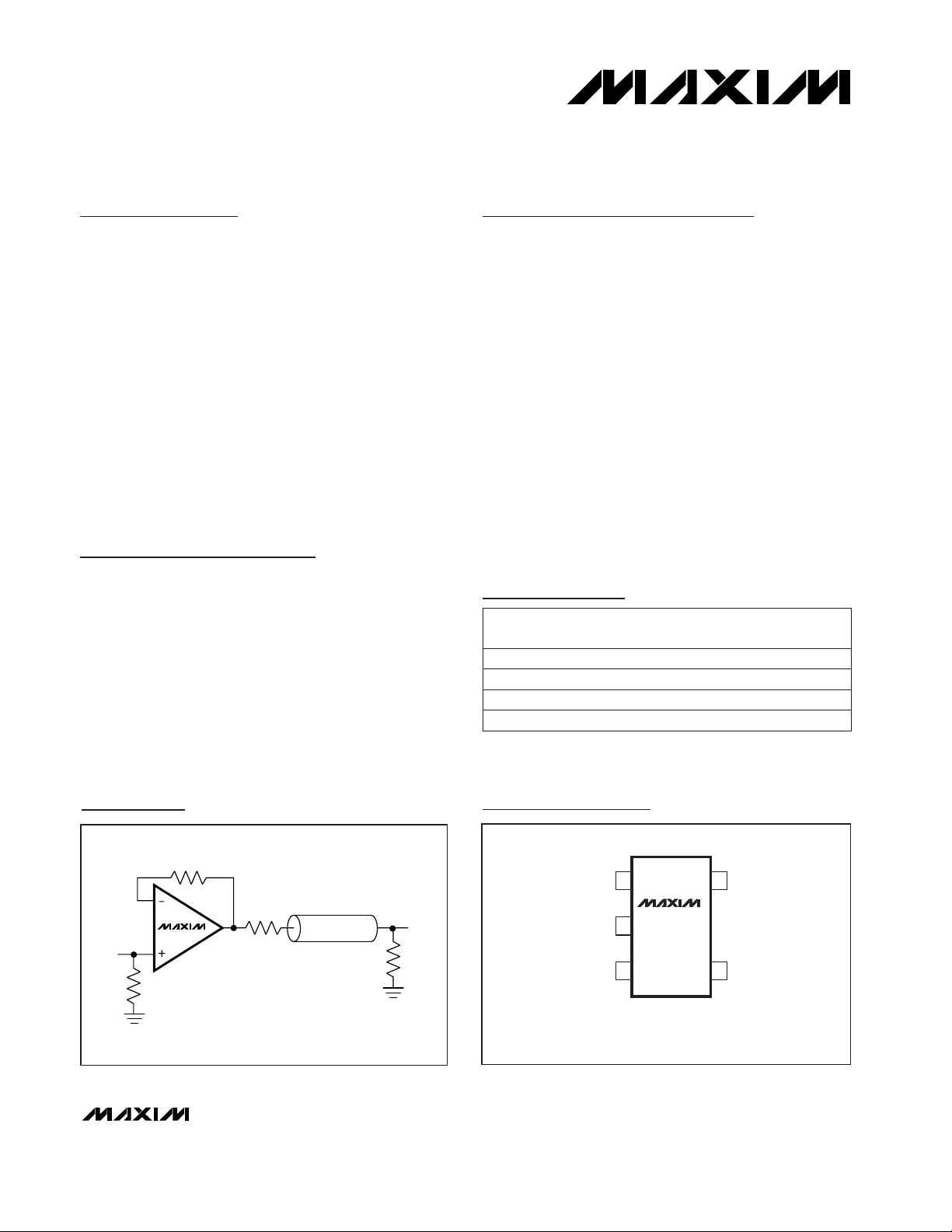
Pin Configurations
R
O
50Ω
IN
V
OUT
ZO = 50Ω
UNITY-GAIN LINE DRIVER
(R
L
= RO + RTO)
R
F
24Ω
R
TO
50Ω
R
TIN
50Ω
MAX4450
Typical Operating Circuit
19-1522; Rev 2; 1/00
Ordering Information
Pin Configurations continued at end of data sheet.
Rail-to-Rail is a registered trademark of Nippon Motorola, Ltd.
PART
MAX4450EXK-T
MAX4450EUK-T
MAX4451EKA-T
MAX4451ESA -40°C to +85°C
-40°C to +85°C
-40°C to +85°C
-40°C to +85°C
TEMP. RANGE
PIN-
PACKAGE
5 SC70-5
5 SOT23-5
8 SOT23-8
8 SO
TOP
MARK
AAA
ADKP
AAAA
—
For free samples and the latest literature, visit www.maxim-ic.com or phone 1-800-998-8800.
For small orders, phone 1-800-835-8769.

MAX4450/MAX4451
Ultra-Small, Low-Cost, 210MHz, Single-Supply
Op Amps with Rail-to-Rail Outputs
2 _______________________________________________________________________________________
ABSOLUTE MAXIMUM RATINGS
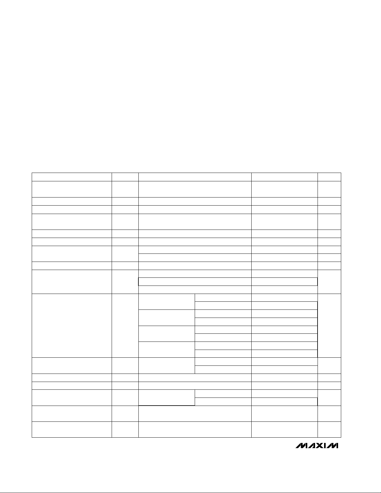
DC ELECTRICAL CHARACTERISTICS
(VCC= +5V, VEE= 0, RL= ∞to VCC/2, V
OUT
= VCC/2, TA= T
MIN
to T
MAX
, unless otherwise noted. Typical values are at TA= +25°C.)
(Note 1)
Supply Voltage (V
CC
to VEE)................................................+12V
IN_-, IN_+, OUT_..............................(V
EE
- 0.3V) to (VCC+ 0.3V)
Output Short-Circuit Current to V
CC
or VEE......................150mA
Continuous Power Dissipation (T
A
= +70°C)
5-Pin SC70-5 (derate 2.5mW/°C above +70°C) ..........200mW
5-Pin SOT23-5 (derate 7.1mW/°C above +70°C)........571mW
8-Pin SOT23-8 (derate 5.26mW/°C above +70°C)......421mW
8-Pin SO (derate 5.9mW/°C above +70°C) .................471mW
Operating Temperature Range ...........................-40°C to +85°C
Storage Temperature Range .............................-65°C to +150°C
Lead Temperature (soldering, 10s) .................................+300°C
Stresses beyond those listed under “Absolute Maximum Ratings” may cause permanent damage to the device. These are stress ratings only, and functional
operation of the device at these or at any other conditions beyond those indicated in the operational sections of the specifications is not implied. Exposure
to absolute maximum rating conditions for extended periods may affect device reliability.
PARAMETER SYMBOL CONDITIONS MIN TYP MAX UNITS
V
VEE-V
CC
0.20 2.25
Guaranteed by CMRR testV
CM
Input Common-Mode
Voltage Range
Input Offset Voltage (Note 2)
Input Offset Voltage Matching
V
OS
426
1.0
mV
mV
µV/°C8TC
VOS
Input Offset Voltage
Temperature Coefficient
Input Bias Current
Input Offset Current
I
B
I
OS
(Note 2)
(Note 2)
6.5 20
0.5 4
µA
µA
kΩ
70Differential mode (-1V ≤ VIN≤ +1V)
R
IN
Input Resistance
Common mode (-0.2V ≤ VCM≤ +2.75V) 3
MΩ
dB70 95
50 60
48 58
57
dB
V
0.05 0.20
0.05 0.15
0.30 0.50
0.25 0.80
0.5 0.80
0.5 1.75
1.0 1.5
0.025 0.065
45 70
mA
mA
Ω8
±120
46 62
dB
V
54 69
4.5 11.0
6.5 9.0 mA
VCCto V
EE
VEE= -5V, VCM= 0
VEE= 0, VCM= 2V
VCC= 5V
Sinking or sourcing
VOL- V
EE
VCC- V
OH
VOL- V
EE
VCC- V
OH
VOL- V
EE
VCC- V
OH
VOL- V
EE
VCC- V
OH
1V ≤ V
OUT
≤ 4V, RL= 50Ω
0.5V ≤ V
OUT
≤ 4.5V, RL= 150Ω
0.25V ≤ V
OUT
≤ 4.75V, RL= 2kΩ
(V
EE
- 0.2V) ≤ V
CM
≤ (V
CC
- 2.25V)
RL= 2kΩ
RL= 150Ω
RL= 75Ω
RL= 75Ω to ground
I
S
V
S
PSRR
R
OUT
I
SC
I
OUT
V
OUT
A
VOL
CMRRCommon-Mode Rejection Ratio
Open-Loop Gain (Note 2)
Output Voltage Swing
(Note 2)
Output Current
Output Short-Circuit Current
Open-Loop Output Resistance
Power-Supply Rejection Ratio
(Note 3)
Operating Supply-Voltage
Range
Quiescent Supply Current
(per amplifier)
RL= 50Ω
25 50
Sourcing
Sinking

MAX4450/MAX4451
Ultra-Small, Low-Cost, 210MHz, Single-Supply
Op Amps with Rail-to-Rail Outputs
_______________________________________________________________________________________ 3
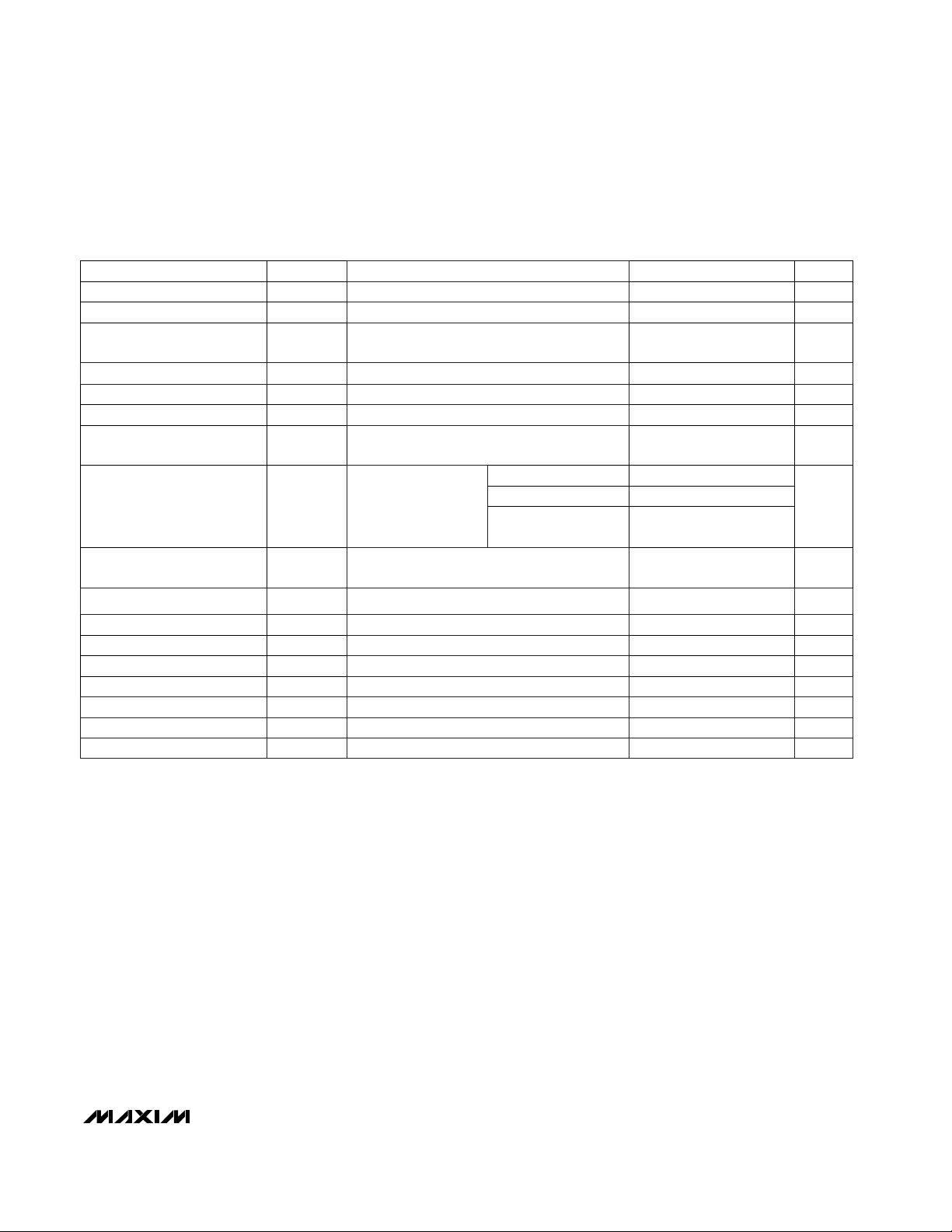
AC ELECTRICAL CHARACTERISTICS
(VCC= +5V, VEE= 0, VCM= +2.5V, RF= 24Ω, RL= 100Ω to VCC/2, V
OUT
= VCC/2, A
VCL
= +1V/V, TA= +25°C, unless otherwise
noted.)
PARAMETER SYMBOL MIN TYP MAX UNITS
2nd harmonic
3rd harmonic
Total harmonic
distortion
Spurious-Free Dynamic
Range
SFDR -65
Bandwidth for 0.1dB Gain
Flatness
BW
0.1dB
55 MHz
Large-Signal -3dB Bandwidth BW
LS
175 MHz
485
Settling Time to 0.1% t
S
16 ns
Rise/Fall Time tR, t
F
4 ns
-65
V
OUT
= 100mVp-p
Small-Signal -3dB Bandwidth BW
SS
210 MHz
dBcfC= 5MHz, V
OUT
= 2Vp-p
Harmonic Distortion HD
-58
-63
dBc
Two-Tone, Third-Order
Intermodulation Distortion
IP3 66 dBc
Input 1dB Compression Point 14 dBm
Differential Phase Error DP 0.08 degrees
Differential Gain Error DG 0.02 %
Input Noise-Voltage Density e
n
10
nV/√Hz
Input Noise-Current Density i
n
1.8
pA/√Hz
Input Capacitance C
IN
1 pF
Output Impedance Z
OUT
1.5
Ω
CONDITIONS
V
OUT
= 2Vp-p
V
OUT
= 2V step
f1 = 4.7MHz, f2 = 4.8MHz, V
OUT
= 1Vp-p
V
OUT
= 100mVp-p
fC= 5MHz,
V
OUT
= 2Vp-p
fC= 10MHz, A
VCL
= +2V/V
NTSC, RL= 150Ω
NTSC, RL= 150Ω
V
OUT
= 100mVp-p
f = 10kHz
f = 10kHz
f = 10MHz
Slew Rate SR V/µsV
OUT
= 2V step
Note 1: All devices are 100% production tested at TA= +25°C. Specifications over temperature limits are guaranteed by design.
Note 2: Tested with V
CM
= +2.5V.
Note 3: PSR for single +5V supply tested with V
EE
= 0, VCC= +4.5V to +5.5V; PSR for dual ±5V supply tested with VEE= -4.5V to
-5.5V, V
CC
= +4.5V to +5.5V.
Channel-to-Channel Isolation CH
ISO
102 dBSpecified at DC

MAX4450/MAX4451
Ultra-Small, Low-Cost, 210MHz, Single-Supply
Op Amps with Rail-to-Rail Outputs
4 _______________________________________________________________________________________
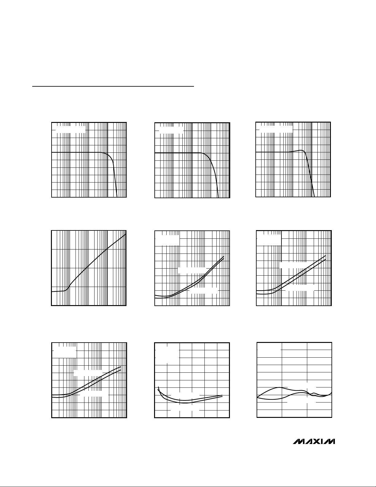
Typical Operating Characteristics
(VCC= +5V, VEE= 0, VCM= +2.5V, A
VCL
= +1V/V, RF= 24Ω, RL= 100Ω to VCC/2, TA = +25°C, unless otherwise noted.)
4
-6
100k 10M 100M1M 1G
SMALL-SIGNAL GAIN vs. FREQUENCY
MAX4450-01
FREQUENCY (Hz)
GAIN (dB)
-5
-4
-3
-2
-1
0
1
2
3
V
OUT
= 100mVp-p
4
-6
100k 10M 100M1M 1G
LARGE-SIGNAL GAIN vs. FREQUENCY
MAX4450-02
FREQUENCY (Hz)
GAIN (dB)
-5
-4
-3
-2
-1
0
1
2
3
V
OUT
= 2Vp-p
0.4
-0.6
100k 10M 100M1M 1G
GAIN FLATNESS vs. FREQUENCY
MAX4450-03
FREQUENCY (Hz)
GAIN (dB)
-0.5
-0.4
-0.3
-0.2
-0.1
0
0.1
0.2
0.3
V
OUT
= 100mVp-p
100k 10M1M 100M 1G
OUTPUT IMPEDANCE vs. FREQUENCY
MAX4450-04
FREQUENCY (Hz)
IMPEDANCE (Ω)
100
0.01
0.1
1
10
2ND HARMONIC
3RD HARMONIC
-10
-100
100k 100M10M1M
DISTORTION vs. FREQUENCY
-70
-90
-30
-50
0
-60
-80
-20
-40
MAX4450-05
FREQUENCY (Hz)
DISTORTION (dBc)
V
OUT
= 2Vp-p
A
VCL
= +1V/V
-10
-100
100k 100M10M1M
DISTORTION vs. FREQUENCY
-70
-90
-30
-50
0
-60
-80
-20
-40
MAX4450-06
FREQUENCY (Hz)
DISTORTION (dBc)
2ND HARMONIC
3RD HARMONIC
V
OUT
= 2Vp-p
A
VCL
= +2V/V
-10
-100
100k 100M10M1M
DISTORTION vs. FREQUENCY
-70
-90
-30
-50
0
-60
-80
-20
-40
MAX4450-07
FREQUENCY (Hz)
DISTORTION (dBc)
2ND HARMONIC
3RD HARMONIC
V
OUT
= 2Vp-p
A
VCL
= +5V/V
-100
-70
-80
-90
-60
-50
-40
-30
-20
-10
0
0 400200 600 800 1000 1200
DISTORTION vs. RESISTIVE LOAD
MAX4450-08
R
LOAD
(Ω)
DISTORTION (dBc)
2ND HARMONIC
3RD HARMONIC
fO = 5MHz
V
OUT
= 2Vp-p
A
VCL
= +1V/V
-100
-70
-80
-90
-60
-50
-40
-30
-20
-10
0
0.5 1.0
1.5
2.0
DISTORTION vs. VOLTAGE SWING
MAX4450-09
VOLTAGE SWING (Vp-p)
DISTORTION (dBc)
fO = 5MHz
A
VCL
= +1V/V
3RD HARMONIC
2ND HARMONIC
 Loading...