

General Description
The MAX4450 single and MAX4451 dual op amps are
unity-gain-stable devices that combine high-speed performance with rail-to-rail outputs. Both devices operate
from a +4.5V to +11V single supply or from ±2.25V to
±5.5V dual supplies. The common-mode input voltage
range extends beyond the negative power-supply rail
(ground in single-supply applications).
The MAX4450/MAX4451 require only 6.5mA of quiescent supply current per op amp while achieving a
210MHz -3dB bandwidth and a 485V/µs slew rate. Both
devices are an excellent solution in low-power/lowvoltage systems that require wide bandwidth, such as
video, communications, and instrumentation.
The MAX4450 is available in the ultra-small 5-pin SC70
package, while the MAX4451 is available in spacesaving 8-pin SOT23 and SO packages.
Applications
Set-Top Boxes
Surveillance Video Systems
Battery-Powered Instruments
Video Line Driver
Analog-to-Digital Converter Interface
CCD Imaging Systems
Video Routing and Switching Systems
Digital Cameras
Features
♦ Ultra-Small SC705 and SOT23 Packages
♦ Low Cost
♦ High Speed
210MHz -3dB Bandwidth
55MHz 0.1dB Gain Flatness
485V/µs Slew Rate
♦ Single +4.5V to +11V Operation
♦ Rail-to-Rail Outputs
♦ Input Common-Mode Range Extends Beyond V
EE
♦ Low Differential Gain/Phase: 0.02%/0.08°
♦ Low Distortion at 5MHz
-65dBc SFDR
-63dB Total Harmonic Distortion
MAX4450/MAX4451
Ultra-Small, Low-Cost, 210MHz, Single-Supply
Op Amps with Rail-to-Rail Outputs
V
EE
IN-
IN+
1
5
V
CC
OUT
MAX4450
SC70/SOT23
TOP VIEW
2
3
4
Pin Configurations
500Ω
500Ω
75Ω
75Ω
IN
OUT
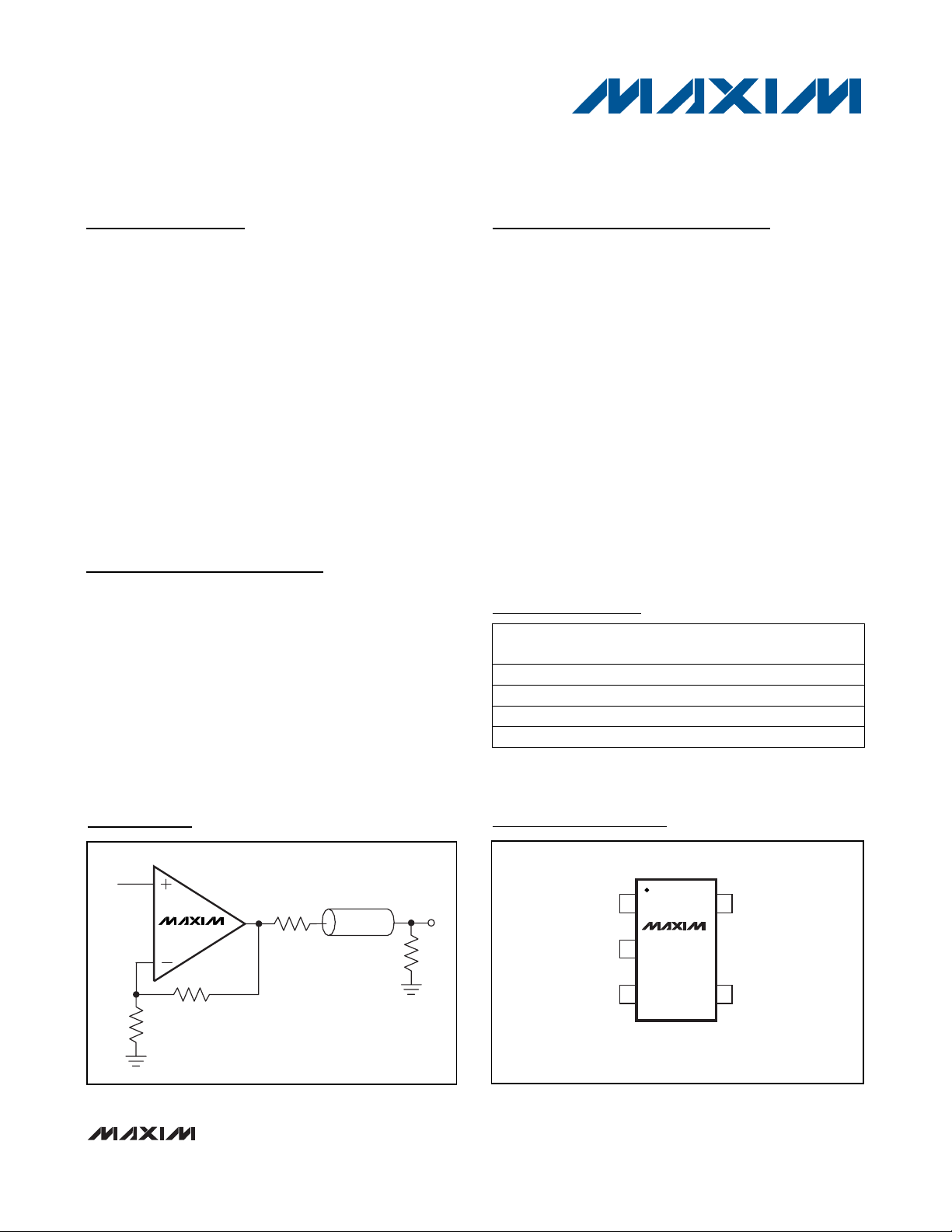
VIDEO LINE DRIVER
Z
o
= 75Ω
MAX4450
Typical Operating Circuit
19-1522; Rev 4; 11/09
Ordering Information
Pin Configurations continued at end of data sheet.
PART
MAX4450EXK-T
MAX4450EUK-T
MAX4451EKA-T
MAX4451ESA -40°C to +85°C
-40°C to +85°C
-40°C to +85°C
-40°C to +85°C
TEMP RANGE
PINPACKAGE
5 SC70
5 SOT23
8 SOT23
8 SO
TOP
MARK
AAA
ADKP
AAAA
—
________________________________________________________________ Maxim Integrated Products 1
For pricing, delivery, and ordering information, please contact Maxim/Dallas Direct! at
1-888-629-4642, or visit Maxim’s website at www.maxim-ic.com.
MAX4450/MAX4451
Ultra-Small, Low-Cost, 210MHz, Single-Supply
Op Amps with Rail-to-Rail Outputs
2 _______________________________________________________________________________________
ABSOLUTE MAXIMUM RATINGS
DC ELECTRICAL CHARACTERISTICS
(VCC= +5V, VEE= 0V, RL= ∞to VCC/2, V
OUT
= VCC/2, TA= T
MIN
to T
MAX
, unless otherwise noted. Typical values are at TA= +25°C.)
(Note 1)
Supply Voltage (V
CC
to VEE)................................................+12V
IN_-, IN_+, OUT_..............................(V
EE
- 0.3V) to (VCC+ 0.3V)
Output Short-Circuit Current to V
CC
or VEE......................150mA
Continuous Power Dissipation (T
A
= +70°C)
5-Pin SC70-5 (derate 2.5mW/°C above +70°C) ..........200mW
5-Pin SOT23-5 (derate 7.1mW/°C above +70°C)........571mW
8-Pin SOT23-8 (derate 5.26mW/°C above +70°C)......421mW
8-Pin SO (derate 5.9mW/°C above +70°C) .................471mW
Operating Temperature Range ...........................-40°C to +85°C
Storage Temperature Range .............................-65°C to +150°C
Lead Temperature (soldering, 10s) .................................+300°C
Stresses beyond those listed under “Absolute Maximum Ratings” may cause permanent damage to the device. These are stress ratings only, and functional
operation of the device at these or at any other conditions beyond those indicated in the operational sections of the specifications is not implied. Exposure
to absolute maximum rating conditions for extended periods may affect device reliability.
PARAMETER SYMBOL CONDITIONS MIN TYP MAX UNITS
V
VEE-V
CC
0.20 2.25
Guaranteed by CMRR testV
CM
Input Common-Mode
Voltage Range
Input Offset Voltage (Note 2)
Input Offset Voltage Matching
V
OS
426
1.0
mV
mV
µV/°C8TC
VOS
Input Offset Voltage
Temperature Coefficient
Input Bias Current
Input Offset Current
I
B
I
OS
(Note 2)
(Note 2)
6.5 20
0.5 4
µA
µA
kΩ
70Differential mode (-1V ≤ VIN≤ +1V)
R
IN
Input Resistance
Common mode (-0.2V ≤ VCM≤ +2.75V) 3
MΩ
dB70 95
50 60
48 58
57
dB
V
0.05 0.20
0.05 0.15
0.30 0.50
0.25 0.80
0.5 0.80
0.5 1.75
45 70
mA
mA
Ω8
±120
46 62
dB
V
54 69
4.5 11.0
6.5 9.0 mA
VCCto V
EE
VEE= -5V, VCM= 0V
VEE= 0V, VCM= 2V
VCC= 5V
Sinking or sourcing
VOL- V
EE
VCC- V
OH
VOL- V
EE
VCC- V
OH
VOL- V
EE
VCC- V
OH
1V ≤ V
OUT
≤ 4V, RL= 50Ω
0.5V ≤ V
OUT
≤ 4.5V, RL= 150Ω
0.25V ≤ V
OUT
≤ 4.75V, RL= 2kΩ
(V
EE
- 0.2V) ≤ V
CM
≤ (V
CC
- 2.25V)
RL= 2kΩ
RL= 150Ω
RL= 75Ω
I
S
V
S
PSRR
R
OUT
I
SC
I
OUT
V
OUT
A
VOL
CMRRCommon-Mode Rejection Ratio
Open-Loop Gain (Note 2)
Output Voltage Swing
(Note 2)
Output Current
Output Short-Circuit Current
Open-Loop Output Resistance
Power-Supply Rejection Ratio
(Note 3)
Operating Supply-Voltage
Range
Quiescent Supply Current
(per amplifier)
RL= 50Ω
25 50
Sourcing
Sinking
MAX4450/MAX4451
Ultra-Small, Low-Cost, 210MHz, Single-Supply
Op Amps with Rail-to-Rail Outputs
_______________________________________________________________________________________ 3
AC ELECTRICAL CHARACTERISTICS
(VCC= +5V, VEE= 0V, VCM= +2.5V, RF= 24Ω, RL= 100Ω to VCC/2, V
OUT
= VCC/2, A
VCL
= +1V/V, TA= +25°C, unless otherwise
noted.)
PARAMETER SYMBOL MIN TYP MAX UNITS
2nd harmonic
3rd harmonic
Total harmonic
distortion
Spurious-Free Dynamic
Range
SFDR -65
Bandwidth for 0.1dB Gain
Flatness
BW
0.1dB
55 MHz
Large-Signal -3dB Bandwidth BW
LS
175 MHz
485
Settling Time to 0.1% t
S
16 ns
Rise/Fall Time tR, t
F
4 ns
-65
V
OUT
= 100mV
P-P
Small-Signal -3dB Bandwidth BW
SS
210 MHz
dBcfC= 5MHz, V
OUT
= 2V
P-P
Harmonic Distortion HD
-58
-63
dBc
Two-Tone, Third-Order
Intermodulation Distortion
IP3 66 dBc
Input 1dB Compression Point 14 dBm
Differential Phase Error DP 0.08 degrees
Differential Gain Error DG 0.02 %
Input Noise-Voltage Density e
n
10
nV/√Hz
Input Noise-Current Density i
n
1.8
pA/√Hz
Input Capacitance C
IN
1 pF
Output Impedance Z
OUT
1.5
Ω
CONDITIONS
V
OUT
= 2V
P-P
V
OUT
= 2V step
f1 = 4.7MHz, f2 = 4.8MHz, V
OUT
= 1V
P-P
V
OUT
= 100mV
P-P
fC= 5MHz,
V
OUT
= 2V
P-P
fC= 10MHz, A
VCL
= +2V/V
NTSC, RL= 150Ω
NTSC, RL= 150Ω
V
OUT
= 100mV
P-P
f = 10kHz
f = 10kHz
f = 10MHz
Slew Rate SR V/µsV
OUT
= 2V step
Note 1: All devices are 100% production tested at TA= +25°C. Specifications over temperature limits are guaranteed by design.
Note 2: Tested with V
CM
= +2.5V.
Note 3: PSR for single +5V supply tested with V
EE
= 0V, VCC= +4.5V to +5.5V; PSR for dual ±5V supply tested with VEE= -4.5V to
-5.5V, V
CC
= +4.5V to +5.5V.
Channel-to-Channel Isolation CH
ISO
102 dBSpecified at DC
MAX4450/MAX4451
Ultra-Small, Low-Cost, 210MHz, Single-Supply
Op Amps with Rail-to-Rail Outputs
4 _______________________________________________________________________________________
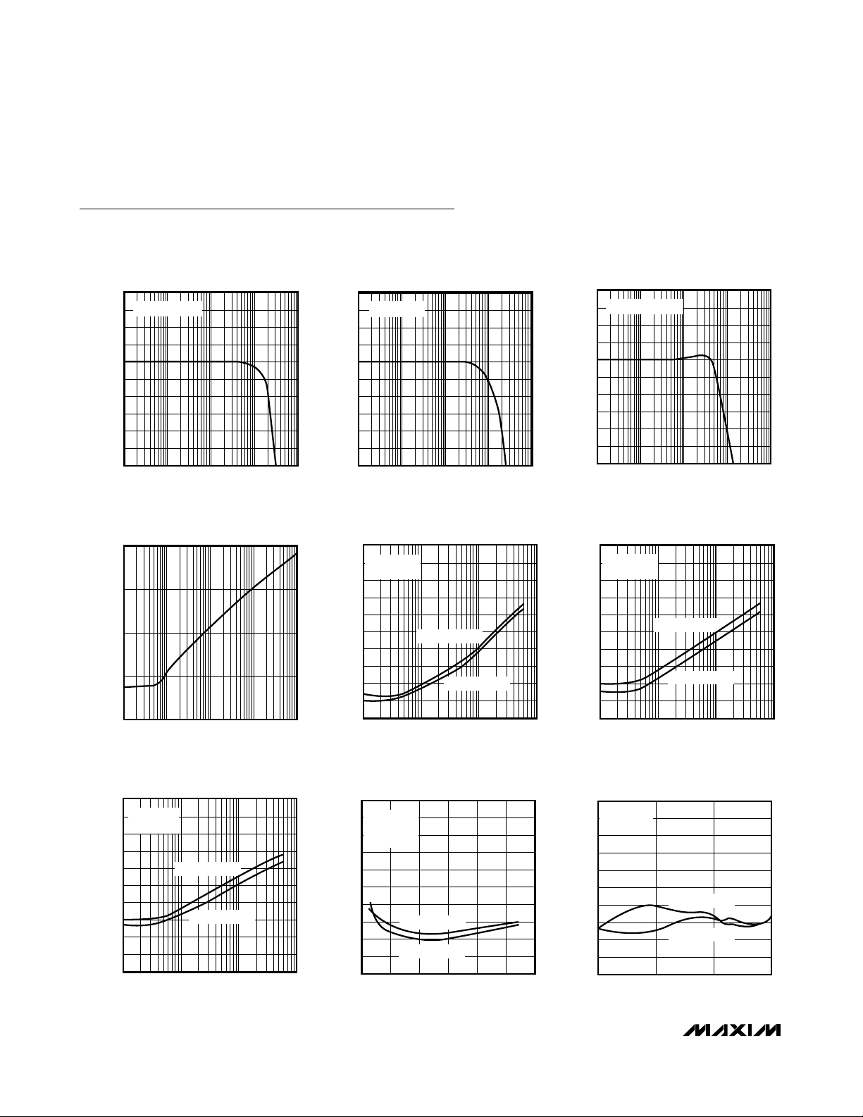
Typical Operating Characteristics
(VCC= +5V, VEE= 0V, VCM= +2.5V, A
VCL
= +1V/V, RF= 24Ω, RL= 100Ω to VCC/2, TA = +25°C, unless otherwise noted.)
4
-6
100k 10M 100M1M 1G
SMALL-SIGNAL GAIN vs. FREQUENCY
MAX4450-01
FREQUENCY (Hz)
GAIN (dB)
-5
-4
-3
-2
-1
0
1
2
3
V
OUT
= 100mV
P-P
4
-6
100k 10M 100M1M 1G
LARGE-SIGNAL GAIN vs. FREQUENCY
MAX4450-02
FREQUENCY (Hz)
GAIN (dB)
-5
-4
-3
-2
-1
0
1
2
3
V
OUT
= 2V
P-P
0.4
-0.6
100k 10M 100M1M 1G
GAIN FLATNESS vs. FREQUENCY
MAX4450-03
FREQUENCY (Hz)
GAIN (dB)
-0.5
-0.4
-0.3
-0.2
-0.1
0
0.1
0.2
0.3
V
OUT
= 100mV
P-P
100k 10M1M 100M 1G
OUTPUT IMPEDANCE vs. FREQUENCY
MAX4450-04
FREQUENCY (Hz)
IMPEDANCE (Ω)
100
0.01
0.1
1
10
2ND HARMONIC
3RD HARMONIC
-10
-100
100k 100M10M1M
DISTORTION vs. FREQUENCY
-70
-90
-30
-50
0
-60
-80
-20
-40
MAX4450-05
FREQUENCY (Hz)
DISTORTION (dBc)
V
OUT
= 2V
P-P
A
VCL
= +1V/V
-10
-100
100k 100M10M1M
DISTORTION vs. FREQUENCY
-70
-90
-30
-50
0
-60
-80
-20
-40
MAX4450-06
FREQUENCY (Hz)
DISTORTION (dBc)
2ND HARMONIC
3RD HARMONIC
V
OUT
= 2V
P-P
A
VCL
= +2V/V
-10
-100
100k 100M10M1M
DISTORTION vs. FREQUENCY
-70
-90
-30
-50
0
-60
-80
-20
-40
MAX4450-07
FREQUENCY (Hz)
DISTORTION (dBc)
2ND HARMONIC
3RD HARMONIC
V
OUT
= 2V
P-P
A
VCL
= +5V/V
-100
-70
-80
-90
-60
-50
-40
-30
-20
-10
0
0 400200 600 800 1000 1200
DISTORTION vs. RESISTIVE LOAD
MAX4450-08
R
LOAD
(Ω)
DISTORTION (dBc)
2ND HARMONIC
3RD HARMONIC
fO = 5MHz
V
OUT
= 2V
P-P
A
VCL
= +1V/V
-100
-70
-80
-90
-60
-50
-40
-30
-20
-10
0
0.5 1.0
1.5
2.0
DISTORTION vs. VOLTAGE SWING
MAX4450-09
VOLTAGE SWING (Vp-p)
DISTORTION (dBc)
fO = 5MHz
A
VCL
= +1V/V
3RD HARMONIC
2ND HARMONIC
MAX4450/MAX4451
Ultra-Small, Low-Cost, 210MHz, Single-Supply
Op Amps with Rail-to-Rail Outputs
_______________________________________________________________________________________ 5
Typical Operating Characteristics (continued)
(VCC= +5V, VEE= 0, VCM= +2.5V, A
VCL
= +1V/V, RF= 24Ω, RL= 100Ω to VCC/2, TA = +25°C, unless otherwise noted.)
DIFFERENTIAL GAIN AND PHASE
0.025
0.020
0.015
0.010
0.005
DIFF GAIN (%)
0
-0.005
-0.010
0100
0.12
0.10
0.08
0.06
0.04
0.02
0
-0.02
DIFF PHASE (degrees)
-0.04
0100
IRE
IRE
OUTPUT VOLTAGE SWING
vs. RESISTIVE LOAD
1.6
1.4
1.2
1.0
0.8
0.6
0.4
OUTPUT VOLTAGE SWING (V)
0.2
0
V
- V
CC
OH
V
- V
OL
EE
0 100 150 200 25050 300 350 400 450 500
R
(Ω)
LOAD
SMALL-SIGNAL PULSE RESPONSE
MAX4450-10
MAX4450-13
COMMON-MODE REJECTION
vs. FREQUENCY
0
-10
-20
-30
-40
-50
CMR (dB)
-60
-70
-80
-90
-100
100k 10M 100M1M 1G
FREQUENCY (Hz)
SMALL-SIGNAL PULSE RESPONSE
INPUT
50mV/div
VOLTAGE (V)
OUTPUT
50mV/div
RF = 24Ω
= +1V/V
A
VCL
20ns/div
LARGE-SIGNAL PULSE RESPONSE
MAX4450-11
MAX4450-14
-10
-20
-30
-40
-50
PSR (dB)
-60
-70
-80
-90
-100
INPUT
25mV/div
VOLTAGE (V)
OUTPUT
50mV/div
POWER-SUPPLY REJECTION
vs. FREQUENCY
0
100k 10M 100M1M 1G
SMALL-SIGNAL PULSE RESPONSE
RF = 500Ω
= +2V/V
A
VCL
LARGE-SIGNAL PULSE RESPONSE
MAX4450-12
FREQUENCY (Hz)
MAX4450-15
20ns/div
INPUT
10mV/div
VOLTAGE (V)
OUTPUT
50mV/div
RF = 500Ω
= +5V/V
A
VCL
MAX4450-17
500mV/div
INPUT
VOLTAGE (V)
OUTPUT
1V/div
RF = 500Ω
= +2V/V
A
VCL
20ns/div
20ns/div
MAX4450-16
INPUT
1V/div
VOLTAGE (V)
OUTPUT
1V/div
RF = 24Ω
= +1V/V
A
VCL
20ns/div
MAX4450-18

MAX4450/MAX4451
Ultra-Small, Low-Cost, 210MHz, Single-Supply
Op Amps with Rail-to-Rail Outputs
6 _______________________________________________________________________________________
Typical Operating Characteristics (continued)
(VCC= +5V, VEE= 0, VCM= +2.5V, A
VCL
= +1V/V, RF= 24Ω, RL= 100Ω to VCC/2, TA = +25°C, unless otherwise noted.)
20ns/div
INPUT
1V/div
INPUT
1V/div
LARGE-SIGNAL PULSE RESPONSE
MAX4450-19
VOLTAGE (V)
RF = 500Ω
A
VCL
= +2V/V
9
11
10
13
12
15
14
16
0 200100 300 40050 250150 350 450 500
ISOLATION RESISTANCE
vs. CAPACITIVE LOAD
MAX4450-22
C
LOAD
(pF)
R
ISO
(Ω)
LARGE SIGNAL (V
OUT
= 2V
P-P
)
SMALL SIGNAL
(V
OUT
= 100mV
P-P
)
0
50
100
150
200
250
300
0200100 300 400 500 600 700 800
SMALL-SIGNAL BANDWIDTH
vs. LOAD RESISTANCE
MAX4450-23
R
LOAD
(Ω)
BANDWIDTH (MHz)
80
0
100 1k 10k
OPEN-LOOP GAIN vs. RESISTIVE LOAD
20
10
MAX4450-24
R
LOAD
(Ω)
OPEN-LOOP GAIN (dBc)
40
30
50
60
70
CURRENT NOISE (pA/√Hz)
1
10k
10010 1k 100k
1M
10M
CURRENT NOISE vs. FREQUENCY
MAX4450-21
FREQUENCY (Hz)
1
10
100
RL = 100Ω
MAX4451
CROSSTALK vs. FREQUENCY
MAX4450-25
FREQUENCY (Hz)
CROSSTALK (dB)
-140
-80
-100
-120
-60
-40
-20
0
20
40
60
0.1M 1M 10M 100M 1G
VOLTAGE NOISE vs. FREQUENCY
100
MAX4450-20
10
VOLTAGE NOISE (nV/√Hz)
RL = 100
1
Ω
1
10010 1k 100k
10k
FREQUENCY (Hz)
1M
10M

Detailed Description
The MAX4450/MAX4451 are single-supply, rail-to-rail,
voltage-feedback amplifiers that employ current-feedback techniques to achieve 485V/µs slew rates and
210MHz bandwidths. Excellent harmonic distortion and
differential gain/phase performance make these amplifiers an ideal choice for a wide variety of video and RF
signal-processing applications.
The output voltage swings to within 55mV of each supply rail. Local feedback around the output stage
ensures low open-loop output impedance to reduce
gain sensitivity to load variations. The input stage permits common-mode voltages beyond the negative supply and to within 2.25V of the positive supply rail.
Applications Information
Choosing Resistor Values
Unity-Gain Configuration
The MAX4450/MAX4451 are internally compensated for
unity gain. When configured for unity gain, the devices
require a 24Ω resistor (RF) in series with the feedback
path. This resistor improves AC response by reducing
the Q of the parallel LC circuit formed by the parasitic
feedback capacitance and inductance.
Inverting and Noninverting Configurations
Select the gain-setting feedback (R
F
) and input (RG)
resistor values to fit your application. Large resistor values increase voltage noise and interact with the amplifier’s input and PC board capacitance. This can
generate undesirable poles and zeros and decrease
bandwidth or cause oscillations. For example, a noninverting gain-of-two configuration (RF= RG) using 1kΩ
resistors, combined with 1pF of amplifier input capacitance and 1pF of PC board capacitance, causes a pole
at 159MHz. Since this pole is within the amplifier bandwidth, it jeopardizes stability. Reducing the 1kΩ resistors to 100Ω extends the pole frequency to 1.59GHz,
but could limit output swing by adding 200Ω in parallel
with the amplifier’s load resistor. Table 1 lists suggested feedback and gain resistors, and bandwidths for
several gain values in the configurations shown in
Figures 1a and 1b.
Layout and Power-Supply Bypassing
These amplifiers operate from a single +4.5V to +11V
power supply or from dual ±2.25V to ±5.5V supplies. For
single-supply operation, bypass V
CC
to ground with a
MAX4450/MAX4451
Ultra-Small, Low-Cost, 210MHz, Single-Supply
Op Amps with Rail-to-Rail Outputs
_______________________________________________________________________________________ 7
Pin Description
PIN
OUT
V
EE
IN+
INA-
OUTA
V
CC
IN-
INB+
INB-
OUTB
INA+
—
4
—
2
1
8
—
5
6
7
3
1 Amplifier Output
2
Negative Power Supply
or Ground (in singlesupply operation)
3 Noninverting Input
—
Amplifier A Inverting
Input
— Amplifier A Output
5 Positive Power Supply
4 Inverting Input
—
Amplifier B Noninverting
Input
—
Amplifier B Inverting
Input
— Amplifier B Output
—
Amplifier A Noninverting
Input
Figure 1a. Noninverting Gain Configuration
Figure 1b. Inverting Gain Configuration
FUNCTION
MAX4450
NAME
MAX4451
R
G
R
F
R
TO
MAX445 _
IN
R
TIN
R
IN
R
TIN
G
R
S
MAX445 _
V
V
= [1+ (RF / RG)] V
OUT
R
F
= -(RF / RG) V
OUT
R
TO
IN
V
OUT
R
IN
O
V
OUT
R
O

Note: RL= RO+ RTO; R
TIN
and RTOare calculated for 50Ω applications. For 75Ω systems, RTO= 75Ω; calculate R
TIN
from the
following equation:
0.1µF capacitor as close to the pin as possible. If operating with dual supplies, bypass each supply with a 0.1µF
capacitor.
Maxim recommends using microstrip and stripline techniques to obtain full bandwidth. To ensure that the PC
board does not degrade the amplifier’s performance,
design it for a frequency greater than 1GHz. Pay careful attention to inputs and outputs to avoid large parasitic capacitance. Whether or not you use a constantimpedance board, observe the following design guidelines:
• Don’t use wire-wrap boards; they are too inductive.
• Don’t use IC sockets; they increase parasitic capacitance and inductance.
• Use surface-mount instead of through-hole components for better high-frequency performance.
• Use a PC board with at least two layers; it should be
as free from voids as possible.
• Keep signal lines as short and as straight as possible. Do not make 90° turns; round all corners.
Rail-to-Rail Outputs,
Ground-Sensing Input
The input common-mode range extends from
(VEE- 200mV) to (VCC- 2.25V) with excellent commonmode rejection. Beyond this range, the amplifier output
is a nonlinear function of the input, but does not undergo phase reversal or latchup.
The output swings to within 55mV of either powersupply rail with a 2kΩ load. The input ground sensing
and the rail-to-rail output substantially increase the
dynamic range. With a symmetric input in a single +5V
application, the input can swing 2.95V
P-P
and the out-
put can swing 4.9V
P-P
with minimal distortion.
Output Capacitive Loading and Stability
The MAX4450/MAX4451 are optimized for AC performance. They are not designed to drive highly reactive
loads, which decrease phase margin and may produce
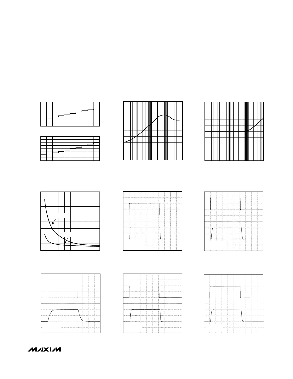
excessive ringing and oscillation. Figure 2 shows a circuit that eliminates this problem. Figure 3 is a graph of
the optimal isolation resistor (RS) vs. capacitive load.
Figure 4 shows how a capacitive load causes excessive peaking of the amplifier’s frequency response if
the capacitor is not isolated from the amplifier by a
resistor. A small isolation resistor (usually 20Ω to 30Ω)
placed before the reactive load prevents ringing and
oscillation. At higher capacitive loads, AC performance
is controlled by the interaction of the load capacitance
and the isolation resistor. Figure 5 shows the effect of a
27Ω isolation resistor on closed-loop response.
Coaxial cable and other transmission lines are easily
driven when properly terminated at both ends with their
characteristic impedance. Driving back-terminated
transmission lines essentially eliminates the line’s
capacitance.
Table 1. Recommended Component Values
MAX4450/MAX4451
Ultra-Small, Low-Cost, 210MHz, Single-Supply
Op Amps with Rail-to-Rail Outputs
8 _______________________________________________________________________________________
-25
+25-10+10-5+5-2+2-1
+1
49.9
10
∞
0
50
1200
GAIN (V/V)
49.9
5
49.9
—
20
500
49.9
15
∞
0
50
500
49.9
11
49.9
—
56
500
49.9
25
100
0
100
500
49.9
25
49.9
—
124
500
49.9
50
62
0
250
500
49.9
95
49.9
—
500
500
49.949.9RTO(Ω)
100210Small-Signal -3dB Bandwidth (MHz)
5649.9R
TIN
(Ω)
0—RS(Ω)
COMPONENT
500
∞
RG(Ω)
50024RF(Ω)
R =
75
1-
75
R
TIN
G
Ω

MAX4450/MAX4451
Ultra-Small, Low-Cost, 210MHz, Single-Supply
Op Amps with Rail-to-Rail Outputs
_______________________________________________________________________________________ 9
Figure 2. Driving a Capacitive Load Through an Isolation Resistor
Figure 3. Capacitive Load vs. Isolation Resistance
Figure 4. Small-Signal Gain vs. Frequency with Load
Capacitance and No Isolation Resistor
Figure 5. Small-Signal Gain vs. Frequency with Load
Capacitance and 27Ω Isolation Resistor
30
25
R
G
R
F
(Ω)
ISO
20
R
ISO
MAX445 _
V
IN
50Ω
R
TIN
V
OUT
C
L
6
5
4
3
2
1
GAIN (dB)
0
-1
-2
-3
-4
100k 10M 100M1M 1G
CL = 10pF
CL = 5pF
FREQUENCY (Hz)
CL = 15pF
15
10
ISOLATION RESISTANCE, R
5
0
500 100 200150 250
CAPACITIVE LOAD, C
(pF)
L
3
R
= 27Ω
ISO
2
1
0
-1
-2
GAIN (dB)
-3
-4
-5
-6
-7
100k 10M 100M1M 1G
CL = 68pF
CL = 120pF
FREQUENCY (Hz)
CL = 47pF

MAX4450/MAX4451
Ultra-Small, Low-Cost, 210MHz, Single-Supply
Op Amps with Rail-to-Rail Outputs
10 ______________________________________________________________________________________
Pin Configurations (continued)
Chip Information
MAX4450 TRANSISTOR COUNT: 86
MAX4451 TRANSISTOR COUNT: 170
TOP VIEW
OUTA
INA+
EE
1
2
MAX4451
3
4
SOT23/SO
87V
6
5
CC
OUTBINA-
INB-
INB+V

MAX4450/MAX4451
Ultra-Small, Low-Cost, 210MHz, Single-Supply
Op Amps with Rail-to-Rail Outputs
______________________________________________________________________________________ 11
PACKAGE TYPE PACKAGE CODE DOCUMENT NO.
5 SC70 X5-1
21-0076
5 SOT23 U5-2
21-0057
8 SOT23 K8-2
21-0078
8 SO S8-5
21-0041
Package Information
For the latest package outline information and land patterns, go to www.maxim-ic.com/packages. Note that a “+”, “#”, or “-” in the
package code indicates RoHS status only. Package drawings may show a different suffix character, but the drawing pertains to the
package regardless of RoHS status.
SC70, 5L.EPS
PACKAGE OUTLINE, 5L SC70
21-0076
1
E
1

MAX4450/MAX4451
Ultra-Small, Low-Cost, 210MHz, Single-Supply
Op Amps with Rail-to-Rail Outputs
12 ______________________________________________________________________________________
Package Information (continued)
For the latest package outline information and land patterns, go to www.maxim-ic.com/packages. Note that a “+”, “#”, or “-” in the
package code indicates RoHS status only. Package drawings may show a different suffix character, but the drawing pertains to the
package regardless of RoHS status.
SOT-23 5L .EPS

MAX4450/MAX4451
Ultra-Small, Low-Cost, 210MHz, Single-Supply
Op Amps with Rail-to-Rail Outputs
______________________________________________________________________________________ 13
Package Information (continued)
For the latest package outline information and land patterns, go to www.maxim-ic.com/packages. Note that a “+”, “#”, or “-” in the
package code indicates RoHS status only. Package drawings may show a different suffix character, but the drawing pertains to the
package regardless of RoHS status.
MARKING
0
0
PACKAGE OUTLINE, SOT-23, 8L BODY
1
21-0078 I
1

MAX4450/MAX4451
Ultra-Small, Low-Cost, 210MHz, Single-Supply
Op Amps with Rail-to-Rail Outputs
14 ______________________________________________________________________________________
Package Information (continued)
For the latest package outline information and land patterns, go to www.maxim-ic.com/packages. Note that a “+”, “#”, or “-” in the
package code indicates RoHS status only. Package drawings may show a different suffix character, but the drawing pertains to the
package regardless of RoHS status.
N
HE
1
e
TOP VIEW
D
A
B
A1
FRONT VIEW
INCHES
DIM
MIN
0.053A
0.004
A1
0.014
B
0.007
C
e 0.050 BSC 1.27 BSC
0.150
E
H 0.2440.228 5.80 6.20
0.016L
VARIATIONS:
INCHES
MINDIM
D
0.189 0.197AA5.004.80 8
0.337 0.344 AB8.758.55 14
D
C
L
0∞- 8∞
MAX
0.069
0.010
0.019
0.010
0.157
0.050
MAX
0.3940.386D
MILLIMETERS
MAX
MIN
1.35
1.75
0.10
0.25
0.35
0.49
0.19
0.25
3.80 4.00
0.401.27
MILLIMETERS
MAX
MIN
9.80 10.00
N MS012
16
AC
SOICN .EPS
SIDE VIEW
PROPRIETARY INFORMATION
TITLE:
PACKAGE OUTLINE, .150" SOIC
21-0041
REV.DOCUMENT CONTROL NO.APPROVAL
1
B
1

Ultra-Small, Low-Cost, 210MHz, Single-Supply
Op Amps with Rail-to-Rail Outputs
Maxim cannot assume responsibility for use of any circuitry other than circuitry entirely embodied in a Maxim product. No circuit patent licenses are
implied. Maxim reserves the right to change the circuitry and specifications without notice at any time.
15 ____________________Maxim Integrated Products, 120 San Gabriel Drive, Sunnyvale, CA 94086 408-737-7600
© 2009 Maxim Integrated Products Maxim is a registered trademark of Maxim Integrated Products, Inc.
Revision History
REVISION
NUMBER
4 11/09 Corrected TOC 20 6
REVISION
DATE
DESCRIPTION
PAGES
CHANGED
 Loading...