

Page 1
General Description
The MAX4434/MAX4435 single and MAX4436/MAX4437
dual operational amplifiers feature wide bandwidth, 16bit settling time in 23ns, and low-noise/low-distortion
operation. The MAX4434/MAX4436 are compensated for
unity-gain stability and have a small-signal -3dB bandwidth of 150MHz. The MAX4435/MAX4437 are compensated for closed-loop gains of +5 or greater and have a
small-signal, -3dB bandwidth of 150MHz.
The MAX4434–MAX4437 op amps require only 15mA of
supply current per amplifier while achieving 115dB
open-loop gain. Voltage noise density is a low 2.2nV/√Hz
and provides 97dB spurious-free dynamic range (SFDR)
at 1MHz. These characteristics make these op amps
ideal for driving modern, high-speed 14- and 16-bit analog-to-digital converters (ADCs).
These high-speed op amps feature wide-output voltage
swings and a high-current output drive up to 65mA. Using
a voltage feedback architecture, the MAX4434–
MAX4437 meet the requirements of many applications
that previously depended on current feedback amplifiers.
The MAX4434/MAX4435 are available in space-saving
5-pin SOT23 packages and the MAX4436/MAX4437 are
available in 8-pin µMAX®packages.
________________________Applications
High-Speed 14- and 16-Bit ADC Preamplifiers
Low-Noise Preamplifiers
IF/RF Amplifiers
Low-Distortion Active Filters
High-Performance Receivers
Precision Instrumentation
____________________________Features
♦ 16-Bit Accurate Settling in 23ns
(MAX4435/MAX4437)
♦ 97dB SFDR at 1MHz, 4Vp-p Output
♦ 2.2nV/√Hz Input Voltage Noise Density
♦ 100dB (min) Open-Loop Gain
♦ 388V/µs Slew Rate (MAX4435/MAX4437)
♦ 65mA High Output Drive
♦ Available in Space-Saving Packages
5-Pin SOT23 (MAX4434/MAX4435)
8-Pin µMAX (MAX4436/MAX4437)
MAX4434–MAX4437
Single-Supply, 150MHz, 16-Bit Accurate,
Ultra-Low Distortion Op Amps
________________________________________________________________ Maxim Integrated Products 1
19-2200; Rev 1; 12/08
Ordering Information
Selector Guide appears at end of data sheet.
IN-IN+
15V
CC
OUT
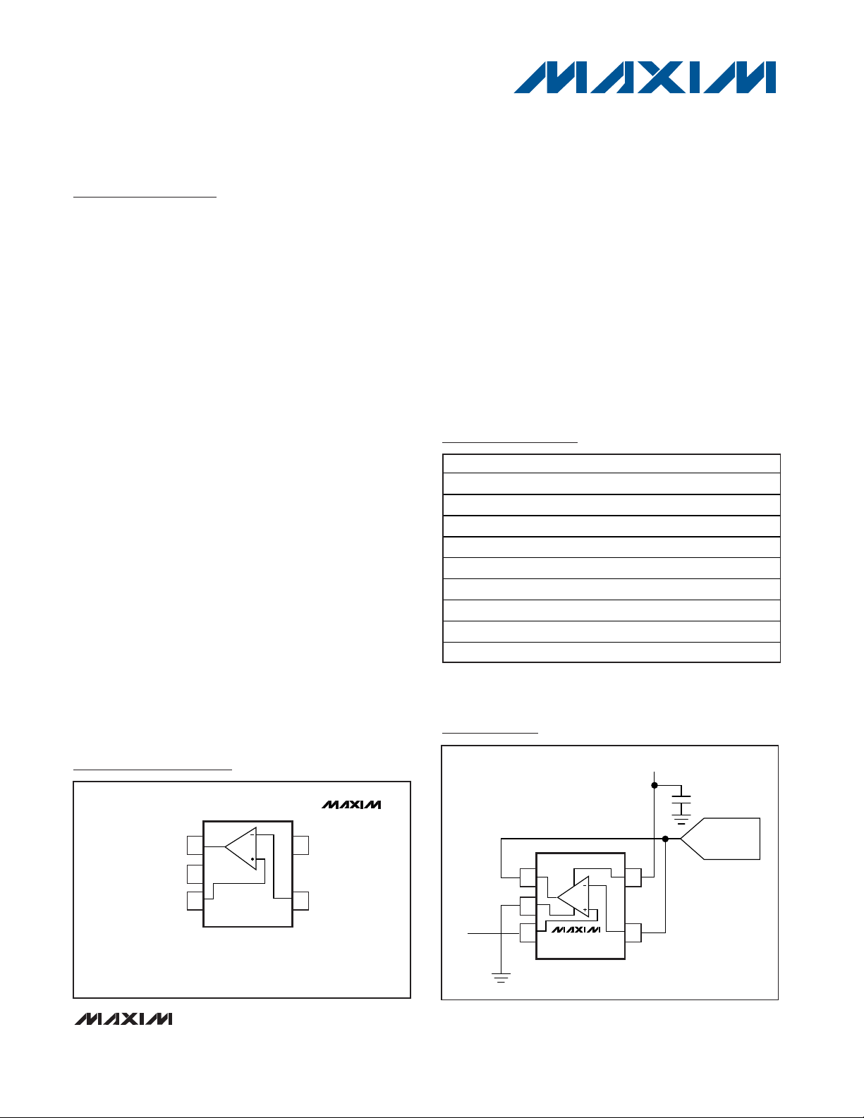
MAX4434
MAX4435
SOT23
TOP VIEW
2
34
V
EE
Pin Configurations
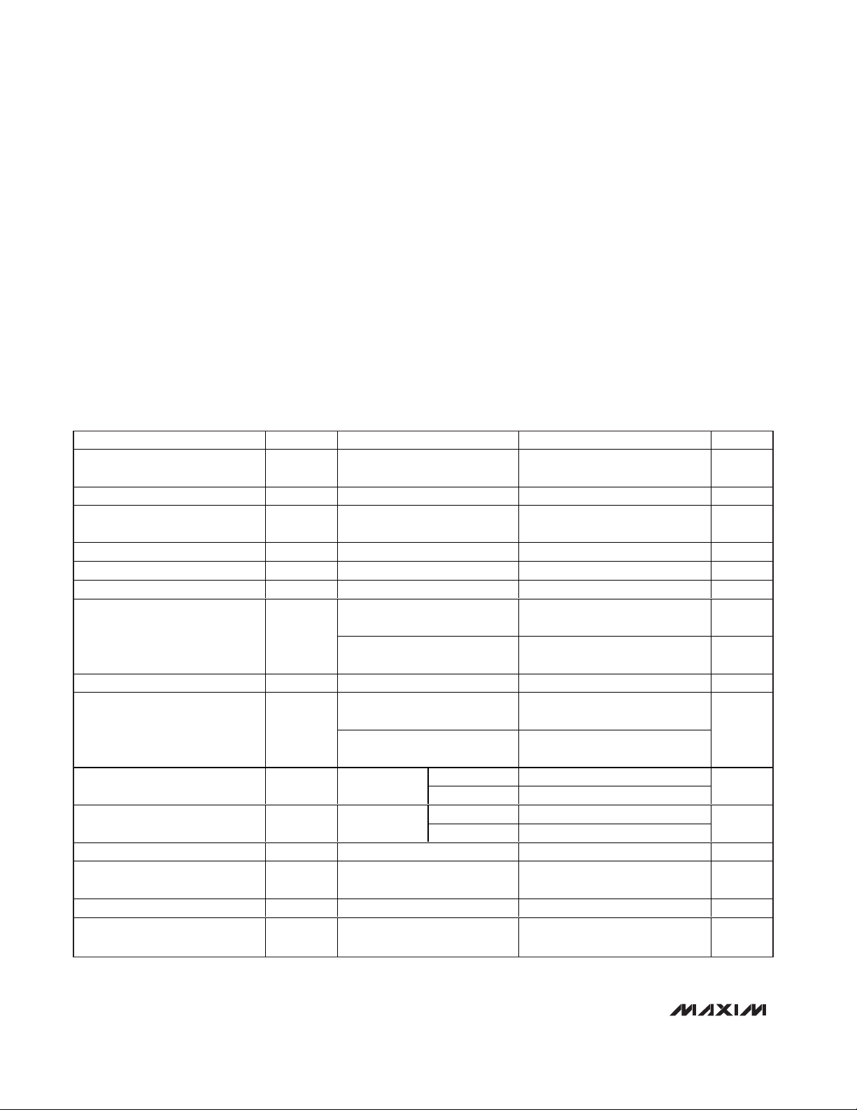
Typical Operating Circuit
IN
15
V
CC
2
34
C
1
HIGH-SPEED
14-/16-BIT ADC
MAX4434
MAX4435
Pin Configurations continued at end of data sheet.
PART TEMP RANGE
PIN-PACKAGE
MAX4434EUK-T -40°C to +85°C 5 SOT23
MAX4434ESA -40°C to +85°C 8 SO
MAX4434EUK/V+T
-40°C to +85°C 5 SOT23
MAX4435EUK-T -40°C to +85°C 5 SOT23
MAX4435ESA -40°C to +85°C 8 SO
MAX4436EUA -40°C to +85°C 8 µMAX
MAX4436ESA -40°C to +85°C 8 SO
MAX4437EUA
-40°C to +85°C 8 µMAX
MAX4437ESA -40°C to +85°C 8 SO
+Denotes a lead(Pb)-free/RoHS-compliant package.
µMAX is a registered trademark of Maxim Integrated Products, Inc.
For pricing, delivery, and ordering information, please contact Maxim Direct at 1-888-629-4642,
or visit Maxim's website at www.maxim-ic.com.
Page 2
MAX4434–MAX4437
Single-Supply, 150MHz, 16-Bit Accurate,
Ultra-Low Distortion Op Amps
2 _______________________________________________________________________________________
ABSOLUTE MAXIMUM RATINGS
DC ELECTRICAL CHARACTERISTICS
(VCC= +5V, VEE= 0, RL= ∞ to VCC/2, TA= T
MIN
to T
MAX
, unless otherwise noted. Typical values are at TA= +25°C.) (Note 2)
Stresses beyond those listed under “Absolute Maximum Ratings” may cause permanent damage to the device. These are stress ratings only, and functional
operation of the device at these or any other conditions beyond those indicated in the operational sections of the specifications is not implied. Exposure to
absolute maximum rating conditions for extended periods may affect device reliability.
Supply Voltage (VCC- VEE) ...................................................+6V
Differential Input Voltage .......................................................+2V
Input Voltage Range ........................(V
CC
+ 0.3V) to (VEE- 0.3V)
Current into Any Input Pin.................................................±25mA
Output Short-Circuit Duration to V
CC
or VEE...................(Note 1)
Continuous Power Dissipation (T
A
= +70°C)
5-Pin SOT23 (derate 7.1mW/°C above +70°C) ..........571mW
8-Pin SO (derate 5.88mW/°C above +70°C)...............471mW
8-Pin µMAX (derate 4.5mW/°C above +70°C) ........... 330mW
Operating Temperature Range ...........................-40°C to +85°C
Junction Temperature......................................................+150°C
Storage Temperature Range .............................-65°C to +150°C
Lead Temperature (soldering, 10s) .................................+300°C
Note 1: The MAX4434–MAX4437 are not protected for output short-circuit conditions.
PARAMETER
SYMBOL
CONDITIONS MIN TYP MAX
UNITS
Input Common-Mode Voltage
Range
V
CM
Guaranteed by CMRR test V
EE
V
Input Offset Voltage V
OS
1 3.5 mV
Input Offset Voltage
Temperature Coefficient
TCV
OS
4 µV/°C
Input Offset Voltage Matching MAX4436/MAX4437 0.25 mV
Input Bias Current I
B
14 22 µA
Input Offset Current I
OS
15µA
Differential Mode
-10mV ≤ V
IN
≤ +10mV
1kΩ
Input Resistance R
IN
Common Mode
0 ≤ V
CM
≤ (V
CC
- 1V)
1.7 MΩ
Common-Mode Rejection Ratio CMRR VEE ≤ V
CM
≤ (V
CC
- 1V) 75 100 dB
(VEE + 0.25) ≤ V
OUT
≤ (V
CC
-
0.25), R
L
= 10kΩ
100 115
Open-Loop Gain A
VOL
(V
EE
+ 0.5) ≤ V
OUT
≤ (V
CC
-
0.5), R
L
= 500Ω
96 110
dB
VCC - V
OH
65 200
Output Voltage Swing V
OUT
RL = 10kΩ
V
OL
- V
EE
15 70
mV
Sinking 40 65
Output Current I
OUT
RL = 20Ω to
Ground
Sourcing 35 60
mA
Output Short-Circuit Current I
SC
Sinking or sourcing ±70 mA
DC Power-Supply Rejection
Ratio
PSRR V
CC
= +4.5V to +5.5V 85 110 dB
Operating Supply Voltage
V
S
Guaranteed by PSRR test +4.5 +5.5 V
Quiescent Supply Current
(Per Amplifier)
I
S
15 18 mA
Note 2: All devices are 100% production tested at +25°C. Specifications over temperature limits are guaranteed by design.
V
- 1
CC
Page 3
MAX4434–MAX4437
Single-Supply, 150MHz, 16-Bit Accurate,
Ultra-Low Distortion Op Amps
_______________________________________________________________________________________ 3
AC ELECTRICAL CHARACTERISTICS
(V
CC
= +5V, VEE= 0, VCM= VCC/2, RL= 500Ω, A
VCL
= +1, and TA= +25°C, unless otherwise noted.)
PARAMETER SYMBOL CONDITIONS
TYP
UNITS
V
OUT
= 20mVp-p
MAX4434/MAX4436
150
Small-Signal -3dB
Bandwidth
BW
SS
V
OUT
= 20mVp-p
MAX4435/MAX4437 (A
VCL
= +5)
150
MHz
V
OUT
= 2Vp-p
MAX4434/MAX4436
28
Large-Signal -3dB
Bandwidth
BW
LS
V
OUT
= 4Vp-p
MAX4435/MAX4437 (A
VCL
= +5)
25
MHz
V
OUT
= 20mVp-p
MAX4434/MAX4436
80
Small-Signal 0.1dB
Gain Flatness
V
OUT
= 20mVp-p
MAX4435/MAX4437 (A
VCL
= +5)
80
MHz
V
OUT
= 2Vp-p
MAX4434/MAX4436
15
Large-Signal 0.1dB
Gain Flatness
V
OUT
= 4Vp-p
MAX4435/MAX4437 (A
VCL
= +5)
20
MHz
V
OUT
= 2V step
MAX4434/MAX4436
133
Slew Rate SR
V
OUT
= 4V step
MAX4435/MAX4437 (A
VCL
= +5)
388
V/µs
V
OUT
= 2V step
MAX4434/MAX4436
17
Rise/Fall Time tR, t
F
V
OUT
= 4V step
MAX4435/MAX4437 (A
VCL
= +5)
10
ns
V
OUT
= 1.5V to 3.5V step
MAX4434/MAX4436
35
V
OUT
= 1.5V to 3.5V step
MAX4435/MAX4437 (A
VCL
= +5)
23
Settling Time to 16-Bit
(0.0015%)
V
OUT
= 1V to 4V step
MAX4434/MAX4436
42
ns
Output “Glitch” Settling
to 16-Bit (0.0015%)
5pF load, C
L
charged from 1V to 4V 41 ns
Output Overload
Recovery Time
50% overdrive, settling to 10% accuracy 100 ns
AC Common-Mode
Rejection Ratio
CMRR f
C
= 100kHz -92 dB
BW
0.1dBSS
BW
0.1dBLS
t
S 0.0015%
MIN
MAX
Page 4
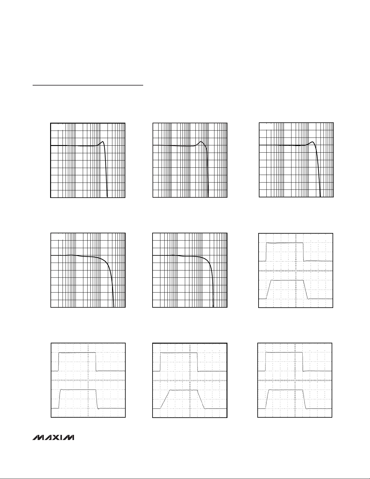
Typical Operating Characteristics
(V
CC
= +5V, VEE= 0, RL= 500Ω, CL= 0, TA= +25°C, unless otherwise noted.)
MAX4434–MAX4437
Single-Supply, 150MHz, 16-Bit Accurate,
Ultra-Low Distortion Op Amps
4 _______________________________________________________________________________________
-7
-4
-5
-6
-3
-2
-1
0
1
2
3
100k 1M 10M 100M 1G
MAX4434/MAX4436
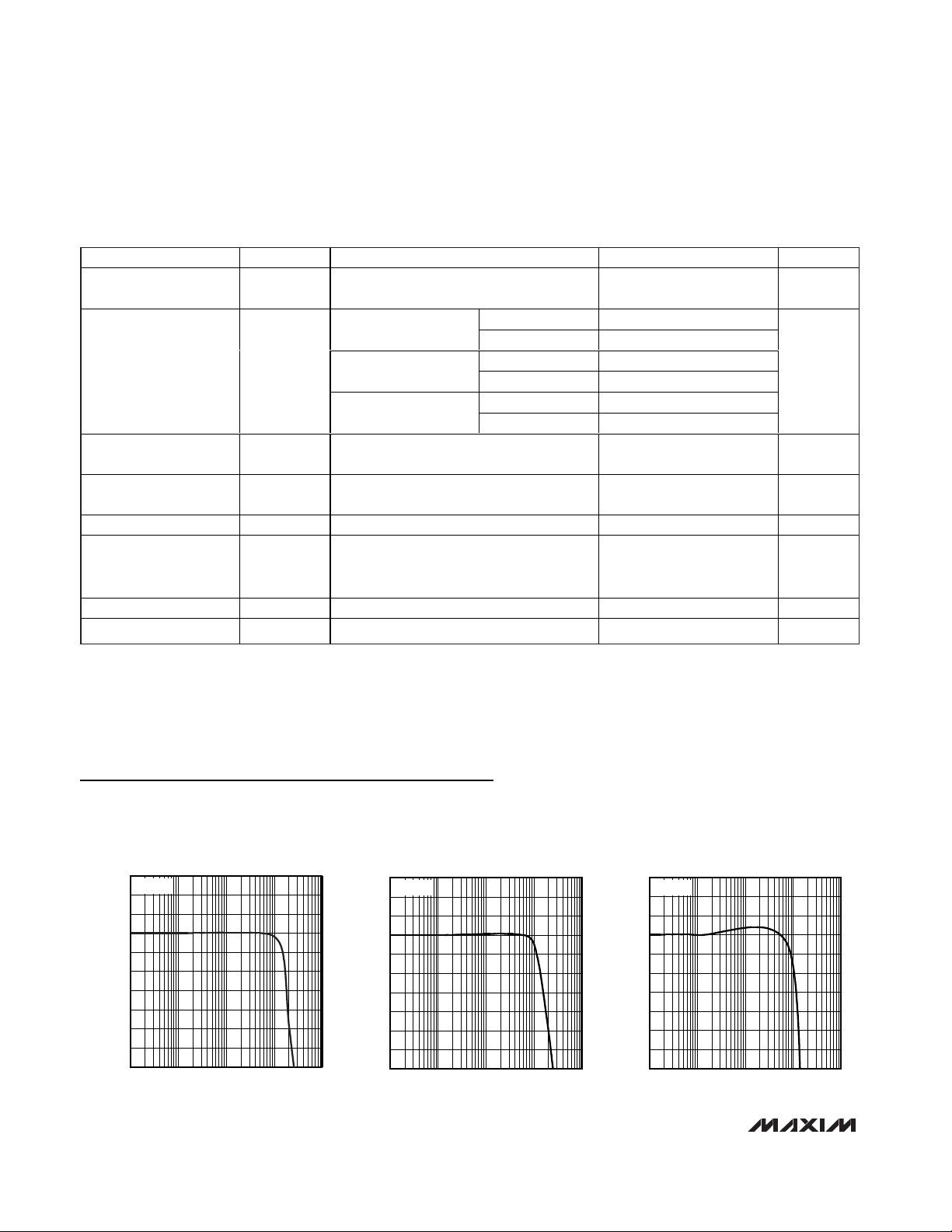
SMALL-SIGNAL GAIN vs. FREQUENCY
(A
VCL
= +1V/V)
MAX4434-37 toc01
FREQUENCY (Hz)
GAIN (dB)
20mVp-p
-7
-4
-5
-6
-3
-2
-1
0
1
2
3
100k 1M 10M 100M 1G
MAX4435/MAX4437
SMALL-SIGNAL GAIN vs. FREQUENCY
(A
VCL
= +5V/V)
MAX4434-37 toc02
FREQUENCY (Hz)
GAIN (dB)
20mVp-p
-0.7
-0.4
-0.5
-0.6
-0.3
-0.2
-0.1
0
0.1
0.2
0.3
100k 1M 10M 100M 1G
MAX4434/MAX4436
GAIN FLATNESS vs. FREQUENCY
(A
VCL
= +1V/V)
MAX4434-37 toc03
FREQUENCY (Hz)
GAIN (dB)
20mVp-p
PARAMETER SYMBOL CONDITIONS
MIN
TYP
MAX
UNITS
AC Power-Supply
Rejection Ratio
PSRR f
C
= 100kHz -101 dB
fC = 100kHz -97
V
OUT
= 2Vp-p
centered at V
CC
/2
f
C
= 1MHz -98
fC = 100kHz -130
V
OUT
= 3Vp-p
centered at V
CC
/2
f
C
= 1MHz -99
fC = 100kHz -112
Spurious-Free Dynamic
Range
SFDR
V
OUT
= 4Vp-p
centered at V
CC
/2
f
C
= 1MHz -97
dBc
Input Noise Voltage
Density
e
n
f
C
= 100kHz 2.2 nV/√Hz
Input Noise Current
Density
i
n
f
C
= 100kHz 2.0 pA/√Hz
Input Capacitance C
IN
2.3 pF
Maximum Capacitive
Load Without Sustained
Oscillations
30 pF
Output Impedance Z
OUT
fC = 1MHz 0.05 Ω
Crosstalk fC = 1MHz, MAX4436/MAX4437 -80 dB
AC ELECTRICAL CHARACTERISTICS (continued)
(V
CC
= +5V, VEE= 0, VCM= VCC/2, RL= 500Ω, A
VCL
= +1, and TA= +25°C, unless otherwise noted.)
Page 5
MAX4434–MAX4437
Single-Supply, 150MHz, 16-Bit Accurate,
Ultra-Low Distortion Op Amps
_______________________________________________________________________________________ 5
-0.7
-0.4
-0.5
-0.6
-0.3
-0.2
-0.1
0
0.1
0.2
0.3
100k 1M 10M 100M
MAX4434/MAX4436
GAIN FLATNESS vs. FREQUENCY
(A
VCL
= +1V/V)
MAX4434-37 toc04
FREQUENCY (Hz)
GAIN (dB)
2Vp-p
10M
MAX4435/MAX4437
GAIN FLATNESS vs. FREQUENCY
(A
VCL
= +5V/V)
0.3
-0.1
MAX4434-37 toc05
-0.3
-0.4
-0.5
-0.6
-0.7
-0.2
0.2
0.1
0
100k
1M 100M
1G
FREQUENCY (Hz)
GAIN (dB)
-0.7
-0.4
-0.5
-0.6
-0.3
-0.2
-0.1
0
0.1
0.2
0.3
100k 1M 10M 100M
MAX4435/MAX4437
GAIN FLATNESS vs. FREQUENCY
(A
VCL
= +5V/V)
MAX4434-37 toc06
FREQUENCY (Hz)
GAIN (dB)
4Vp-p
MAX4434/MAX4436
LARGE-SIGNAL GAIN vs. FREQUENCY
(A
VCL
= +1V/V)
3
-1
MAX4434-37 toc07
-3
-4
-5
-6
-7
-2
2
1
0
100k
1M 10M
100M
FREQUENCY (Hz)
GAIN (dB)
2Vp-p
-7
-4
-5
-6
-3
-2
-1
0
1
2
3
100k 1M 10M 100M
MAX4435/MAX4437
LARGE-SIGNAL GAIN vs. FREQUENCY
(A
VCL
= +5V/V)
MAX4434-37 toc08
FREQUENCY (Hz)
GAIN (dB)
MAX4434/MAX4436
SMALL-SIGNAL PULSE RESPONSE
MAX4434-47 toc09
INPUT
50mV/div
OUTPUT
50mV/div
20ns/div
A
VCL
= +1V/V
MAX4435/MAX4437
SMALL-SIGNAL PULSE RESPONSE
MAX4434-47 toc10
INPUT
10mV/div
OUTPUT
50mV/div
20ns/div
A
VCL
= +5V/V
MAX4434/MAX4436
LARGE-SIGNAL PULSE RESPONSE
MAX4434-47 toc11
INPUT
1V/div
OUTPUT
1V/div
20ns/div
A
VCL
= +1V/V
MAX4435/MAX4437
LARGE-SIGNAL PULSE RESPONSE
MAX4434-47 toc12
INPUT
200mV/div
OUTPUT
1V/div
20ns/div
A
VCL
= +5V/V
Typical Operating Characteristics (continued)
(V
CC
= +5V, VEE= 0, RL= 500Ω, CL= 0, TA= +25°C, unless otherwise noted.)
Page 6

MAX4434–MAX4437
Single-Supply, 150MHz, 16-Bit Accurate,
Ultra-Low Distortion Op Amps
6 _______________________________________________________________________________________
MAX4435/MAX4437
SMALL-SIGNAL PULSE RESPONSE
MAX4434-47 toc14
INPUT
10mV/div
OUTPUT
50mV/div
20ns/div
AV = +5V/V
C
L
= 15pF
MAX4434/MAX4436
SMALL-SIGNAL PULSE RESPONSE
MAX4434-47 toc13
INPUT
50mV/div
OUTPUT
50mV/div
20ns/div
A
VCL
= +1V/V
C
L
= 15pF
MAX4434/MAX4436
LARGE-SIGNAL PULSE RESPONSE
MAX4434-47 toc15
INPUT
1V/div
OUTPUT
1V/div
20ns/div
A
VCL
= +1V/V
C
L
= 30pF
MAX4435/MAX4437
LARGE-SIGNAL PULSE RESPONSE
MAX4434-47 toc16
INPUT
200mV/div
OUTPUT
1V/div
20ns/div
A
VCL
= +5V/V
C
L
= 30pF
-110
-90
-50
-70
-30
-10
POWER-SUPPLY REJECTION RATIO
vs. FREQUENCY
MAX4434-37 toc17
FREQUENCY (MHz)
POWER-SUPPLY REJECTION RATIO (dB)
0.1 101100
-100
-70
-80
-90
-60
-50
-40
-30
-20
-10
0
0.1 101 100
COMMON-MODE REJECTION RATIO
vs. FREQUENCY
MAX4434-37 toc18
FREQUENCY (MHz)
COMMON-MODE REJECTION RATIO (dB)
0
4
2
8
6
10
12
0 10050 150 200
OUTPUT ISOLATION RESISTANCE
vs. CAPACITIVE LOAD
MAX4434-37 toc19
CAPACITIVE LOAD (pF)
OUTPUT ISOLATION RESISTANCE (Ω)
MAX4434/MAX4436
MAX4435/MAX4437
100
10
1
0.1
0.01
0.1 101 100 1000
CLOSED-LOOP OUTPUT IMPEDANCE
vs. FREQUENCY
MAX4434-37 toc20
FREQUENCY (MHz)
OUTPUT IMPEDANCE (Ω)
-60
-30
-40
-50
-20
-10
0
10
20
30
40
50
60
70
-270
-135
-180
-225
-90
-45
0
45
90
135
180
225
270
315
GAIN AND PHASE vs. FREQUENCY
MAX4434-37 toc21
FREQUENCY (Hz)
GAIN (dB)
PHASE (degrees)
10k 1M100k 10M 100M 1G
GAIN
PHASE
A
VCL
= 1000V/V
Typical Operating Characteristics (continued)
(V
CC
= +5V, VEE= 0, RL= 500Ω, CL= 0, TA= +25°C, unless otherwise noted.)
Page 7

-110
-100
-90
-80
-70
-60
-50
-40
-30
-20
-10
0
HARMONIC DISTORTION
vs. RESISTIVE LOAD
MAX4434-37 toc24
RESISTIVE LOAD (Ω)
HARMONIC DISTORTION (dB)
0 1000500 1500 2000 2500
V
OUT
= 1Vp-p
f = 500kHz
2ND HARMONIC
3RD HARMONIC
MAX4434–MAX4437
Single-Supply, 150MHz, 16-Bit Accurate,
Ultra-Low Distortion Op Amps
_______________________________________________________________________________________ 7
-110
-90
-100
-70
-80
-60
-50
0.1110
HARMONIC DISTORTION
vs. FREQUENCY
MAX4434-37 toc22
FREQUENCY (MHz)
HARMONIC DISTORTION (dB)
V
OUT
= 2Vp-p
2ND HARMONIC
3RD HARMONIC
-130
-110
-100
-120
-80
-90
-50
-60
-70
-40
HARMONIC DISTORTION
vs. OUTPUT SWING
MAX4434-37 toc23
OUTPUT SWING (Vp-p)
HARMONIC DISTORTION (dB)
0
1.0
0.5
2.0
1.5
2.5
4.0
f = 500kHz
2ND HARMONIC
3RD HARMONIC
3.0
3.5
100
10
1
11k10 100 10k 100k 1M
INPUT VOLTAGE NOISE
vs. FREQUENCY
MAX4434-37 toc25
FREQUENCY (Hz)
VOLTAGE NOISE (nV/√Hz)
100
10
1
11k10 100 10k 100k 1M
INPUT CURRENT NOISE DENSITY
vs. FREQUENCY
MAX4434-37 toc26
FREQUENCY (Hz)
CURRENT NOISE DENSITY (pA/√Hz)
-120
-80
-100
-40
-60
-20
0
0.1 101 100 1000
MAX4436/MAX4437
CROSSTALK vs. FREQUENCY
MAX4434-37 toc27
FREQUENCY (MHz)
GAIN (dB)
10
12
11
14
13
15
16
QUIESCENT CURRENT PER AMPLIFIER
vs. TEMPERATURE
MAX4434-37 toc28
TEMPERATURE (°C)
QUIESCENT CURRENT (mA)
-25-50 0 25 50 75 100
5
8
7
6
9
10
11
12
13
14
15
-50 0-25 255075100
BIAS CURRENT
vs. TEMPERATURE
MAX4434-37 toc29
TEMPERATURE (°C)
BIAS CURRENT (μA)
-1.0
-0.4
-0.6
-0.8
-0.2
0
0.2
0.4
0.6
0.8
1.0
-50 0-25 25 50 75 100
OFFSET VOLTAGE
vs. TEMPERATURE
MAX4434-37 toc30
TEMPERATURE (°C)
OFFSET VOLTAGE (mV)
Typical Operating Characteristics (continued)
(V
CC
= +5V, VEE= 0, RL= 500Ω, CL= 0, TA= +25°C, unless otherwise noted.)
Page 8

PIN
MAX4436/MAX4437
SO/µMAX
NAME
FUNCTION
1 OUTA Amplifier A Output
2 INA- Amplifier A Inverting Input
3 INA+ Amplifier A Noninverting Input
4V
EE
Ground
5 INB+ Amplifier A Noninverting Input
6 INB- Amplifier A Inverting Input
7 OUTB Amplifier A Output
8V
CC
Positive Power Supply
Pin Description
MAX4434–MAX4437
Single-Supply, 150MHz, 16-Bit Accurate,
Ultra-Low Distortion Op Amps
8 _______________________________________________________________________________________
0
30
90
60
120
150
-50 0-25 255075100
VOLTAGE SWING
vs. TEMPERATURE
MAX4434-37 toc31
TEMPERATURE (°C)
VOLTAGE SWING (mV)
FROM POSITIVE
FROM NEGATIVE
0
20
60
40
80
100
-50 0-25 25 50 75 100
VOLTAGE SWING
vs. TEMPERATURE
MAX4434-37 toc32
TEMPERATURE (°C)
VOLTAGE SWING (mV)
FROM POSITIVE RAIL
FROM NEGATIVE RAIL
RL = 10k
Ω
Typical Operating Characteristics (continued)
(V
CC
= +5V, VEE= 0, RL= 500Ω, CL= 0, TA= +25°C, unless otherwise noted.)
PIN
MAX4434/MAX4435
NAME FUNCTION
SOT23 SO
1 6 OUT Output
24V
EE
Ground
3 3 IN+ Noninverting Input
4 2 IN- Inverting Input
57V
CC
Positive Power Supply
— 1, 5, 8 N.C. No Connection. Not internally connected.
Page 9

MAX4434–MAX4437
Single-Supply, 150MHz, 16-Bit Accurate,
Ultra-Low Distortion Op Amps
_______________________________________________________________________________________ 9
Detailed Description
The MAX4434–MAX4437 are wide-bandwidth, ultra-lowdistortion, voltage-feedback amplifiers. The MAX4434/
MAX4436 are internally compensated for unity gain.
The MAX4435/MAX4437 are internally compensated for
gains of +5V/V or greater.
These amplifiers have ultra-fast 35ns (MAX4434/
MAX4436) 16-bit settling times, -97dB SFDR at 1MHz,
and 4Vp-p output swing with minimum 115dB openloop gain.
High-Speed ADC Input Driver Application
The MAX4434–MAX4437 op amps are ideal for driving
high-speed 14- to 16-bit ADCs. In most cases, these
ADCs operate with a charge balance scheme, with
capacitive loads internally switched on and off from the
input. The driver used must withstand these changing
capacitive loads while holding the signal amplitude stability consistent with the ADC’s resolution and, at the
same time, have a frequency response compatible with
the sampling speed of the ADC (Figure 1).
Inverting and Noninverting Configurations
The circuits typically used for the inverting and noninverting configurations of the MAX4434–MAX4437 are
shown in Figures 2a and 2b. The minimum unconditionally stable gain values are 1 for the MAX4434/MAX4436
and 5 for the MAX4435/MAX4437. Use care in selecting
the value for the resistor marked R
S
in both circuits. From
dynamic stability considerations (based on the part’s frequency response and the input capacitance of the
MAX4434–MAX4437), the maximum recommended
value for RSis 500Ω. In general, lower RSvalues will
yield a higher bandwidth and better dynamic stability, at
the cost of higher power consumption, higher power dissipation in the IC, and reduced output drive availability.
For a minimum RS value, take into consideration that the
current indicated as IFis supplied by the output stage
and must be discounted from the maximum output current to calculate the maximum current available to the
load. IFcan be found using the following equation:
IF= V
IN(MAX)
/ R
S
If DC thermal stability is an important design concern,
the Thevenin resistance seen by both inputs at DC
must be balanced. This includes the resistance of the
signal source and termination resistors if the amplifier
signal input is fed from a transmission line. The capacitance associated with the feedback resistors must also
be considered as a possible limitation to the available
bandwidth or to the dynamic stability. Only resistors
with small parallel capacitance specifications should
be considered.
Applications Information
Layout and Power-Supply Bypassing
The MAX4434–MAX4437 have wide bandwidth and
consequently require careful board layout. To realize
the full AC performance of these high-speed amplifiers,
pay careful attention to power-supply bypassing and
board layout. The PC board should have a large lowimpedance ground plane that is as free of voids as
possible. Do not use commercial breadboards. Keep
signal lines as short and straight as possible. Observe
high-frequency bypassing techniques to maintain the
amplifier’s accuracy and stability. In general, use sur-
V
CC
V
EE
HIGH-SPEED
14/16-BIT ADC
Figure 1. Typical Application Circuit
V
OUT
V
IN
R
S
R
F
I
F
R
F
R
S
V
OUT
V
IN
=A = 1 +
Figure 2a. Noninverting Configuration
- R
F
R
S
V
OUT
V
IN
V
OUT
V
IN
R
B
R
F
R
S
I
F
= A =
Figure 2b. Inverting Configuration
Page 10

MAX4434–MAX4437
Single-Supply, 150MHz, 16-Bit Accurate,
Ultra-Low Distortion Op Amps
10 ______________________________________________________________________________________
face-mount components since they have shorter bodies
and lower parasitic reactance. This will result in
improved performance over through-hole components.
The bypass capacitors should include 1nF and/or
0.1µF surface-mount ceramic capacitors between V
CC
and the ground plane, located as close to the package
as possible. Place a 10µF tantalum capacitor at the
power supply’s point of entry to the PC board to ensure
the integrity of the incoming supplies. Input termination
resistors and output back-termination resistors, if used,
should be surface-mount types and should be placed
as close to the IC pins as possible.
Driving Capacitive Loads
The MAX4434–MAX4437 can drive capacitive loads.
However, excessive capacitive loads may cause ringing or instability at the output as phase margin is
reduced. Adding a small isolation resistor in series with
the output capacitive load helps reduce the ringing but
slightly increases gain error (see Typical Operating
Characteristics and Figure 3).
MAX4434MAX4437
V
OUT
V
IN
R
ISO
C
L
R
L
Figure 3. Capacitive-Load Driving Circuit
Selector Guide
PART
AMPS
MIN GAIN
(V/V)
BW
(MHz)
SETTLING
TIME TO
0.0015%
(ns)
MAX4434
1+1
150
35
MAX4435
1+5
150
23
MAX4436
2+1
150
35
MAX4437
2+5
150
23
Pin Configurations (continued)
TOP VIEW
1
2
3
4
8
7
6
5
V
CC
OUTB
INB-
INB+V
EE
INA+
INA-
OUTA
MAX4436
MAX4437
μMAX/SO
1
2
3
4
8
7
6
5
N.C.
V
CC
OUT
N.C.V
EE
IN+
IN-
N.C.
SO
MAX4434
MAX4435
Chip Information
MAX4434/MAX4435 TRANSISTOR COUNT: 141
MAX4436/MAX4437 TRANSISTOR COUNT: 318
STABLE
Page 11

MAX4434–MAX4437
Single-Supply, 150MHz, 16-Bit Accurate,
Ultra-Low Distortion Op Amps
______________________________________________________________________________________ 11
Package Information
(For the latest package outline information and land patterns, go to www.maxim-ic.com/packages.)
PACKAGE TYPE PACKAGE CODE DOCUMENT NO.
5 SOT23 U5-1 21-0057
8 SO S8-2 21-0036
8 µMAX U8-1 21-0041
SOT-23 5L .EPS
Page 12

MAX4434–MAX4437
Single-Supply, 150MHz, 16-Bit Accurate,
Ultra-Low Distortion Op Amps
12 ______________________________________________________________________________________
Package Information (continued)
(For the latest package outline information and land patterns, go to www.maxim-ic.com/packages.)
α
8LUMAXD.EPS
α
Page 13

MAX4434–MAX4437
Single-Supply, 150MHz, 16-Bit Accurate,
Ultra-Low Distortion Op Amps
______________________________________________________________________________________ 13
Package Information (continued)
(For the latest package outline information and land patterns, go to www.maxim-ic.com/packages.)
SOICN .EPS
PACKAGE OUTLINE, .150" SOIC
1
1
21-0041
B
REV.DOCUMENT CONTROL NO.APPROVAL
PROPRIETARY INFORMATION
TITLE:
TOP VIEW
FRONT VIEW
MAX
0.010
0.069
0.019
0.157
0.010
INCHES
0.150
0.007
E
C
DIM
0.014
0.004
B
A1
MIN
0.053A
0.19
3.80 4.00
0.25
MILLIMETERS
0.10
0.35
1.35
MIN
0.49
0.25
MAX
1.75
0.050
0.016L
0.40 1.27
0.3940.386D
D
MINDIM
D
INCHES
MAX
9.80 10.00
MILLIMETERS
MIN
MAX
16
AC
0.337 0.344 AB8.758.55 14
0.189 0.197 AA5.004.80 8
N MS012
N
SIDE VIEW
H 0.2440.228 5.80 6.20
e 0.050 BSC 1.27 BSC
C
HE
e
B
A1
A
D
0∞-8∞
L
1
VARIATIONS:
Page 14

MAX4434–MAX4437
Single-Supply, 150MHz, 16-Bit Accurate,
Ultra-Low Distortion Op Amps
Maxim cannot assume responsibility for use of any circuitry other than circuitry entirely embodied in a Maxim product. No circuit patent licenses are
implied. Maxim reserves the right to change the circuitry and specifications without notice at any time.
14 ____________________Maxim Integrated Products, 120 San Gabriel Drive, Sunnyvale, CA 94086 408-737-7600
© 2008 Maxim Integrated Products is a registered trademark of Maxim Integrated Products, Inc.
Revision History
REVISION
NUMBER
REVISION
DATE
DESCRIPTION
PAGES
CHANGED
0 10/01 Initial release —
1 12/08 Added automotive part number 1
 Loading...