

Page 1
EVALUATION KIT AVAILABLE
19-6157; Rev 1; 4/12
MAX44280
1.8V, 50MHz, Low-Offset,
Low-Power, Rail-to-Rail I/O Op Amp
General Description
The MAX44280 offers a unique combination of high
speed, precision, low noise, and low-voltage operation
making it ideally suited for a large number of signal processing functions such as filtering and amplification of
signals in portable and industrial equipment.
The amplifier features an input offset of less than 50FV
and a high-gain bandwidth product of 50MHz while
maintaining a low 1.8V supply rail. The device is internally
compensated for gains of 5V/V or greater. The device’s
rail-to-rail input/outputs and low noise guarantee maximum dynamic range in demanding applications such
as 12- to 16-bit SAR ADC drivers. Unlike traditional
rail-to-rail input structures, input crossover distortion is
absent due to an optimized input stage with an ultra-quiet
charge pump.
The MAX44280 includes a fast-power-on shutdown mode
for further power savings.
The MAX44280 operates from a supply range of 1.8V to
5.5V over the -40NC to +125NC temperature range and
can operate down to 1.7V over the 0NC to +70NC temperature range. The MAX44280 is available in a small,
6-pin SC70 package and is also available in a 1mm x
1.5mm thin µDFN (ultra-thin LGA) package.
Ordering Information appears at end of data sheet.
Features
S Low 1.8V Supply Rail Over the -40°C to +125°C
Range
S 1.7V Supply Rail Over the 0°C to +70°C Range
S 50MHz Bandwidth
S Low 12.7nV/√Hz Input Voltage-Noise Density
S Low 1.2fA/√Hz Input Current-Noise Density
S Low 50µV (max) VOS at +25°C
S 500fA Low Input Bias Current
S 750µA Quiescent Current per Amplifier
S < 1µA Supply Current in Shutdown
S Small, 2mm x 2mm SC70 and 1mm x 1.5mm Thin
µDFN Packages
S Low 110dB Total Harmonic Distortion
S 5V/V Minimum Stable Gain
Applications
Notebooks
3G/4G Handsets
Portable Media Players
Portable Medical Instruments
Battery-Operated Devices
Analog-to-Digital Converter Buffers
Transimpedance Amplifiers
General-Purpose Signal Processing
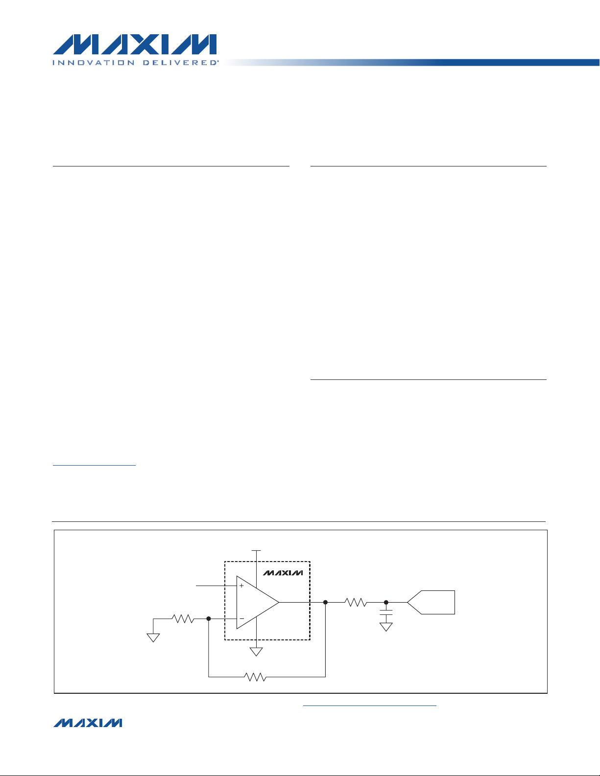
Typical Application Circuit
+3.3V
24kI
MAX44280
10kI
3.3nF
ADC
MAX11645
V
SIG
2.4kI
For related parts and recommended products to use with this part, refer to: www.maxim-ic.com/MAX44280.related
����������������������������������������������������������������� Maxim Integrated Products 1
For pricing, delivery, and ordering information, please contact Maxim Direct at 1-888-629-4642,
or visit Maxim’s website at www.maxim-ic.com.
Page 2
MAX44280
1.8V, 50MHz, Low-Offset,
Low-Power, Rail-to-Rail I/O Op Amp
ABSOLUTE MAXIMUM RATINGS
IN+, IN-, OUT .................................(VSS - 0.3V) to (VDD + 0.3V)
V
to VSS ............................................................... -0.3V to +6V
DD
SHDN .......................................................................-0.3V to +6V
Output to Short-Circuit Ground Duration .............................. 10s
Continuous Input Current into Any Pin ............................ Q20mA
Continuous Power Dissipation (TA = +70NC)
SC70 (derate 3.1mW/NC above +70NC) ......................245mW
Stresses beyond those listed under “Absolute Maximum Ratings” may cause permanent damage to the device. These are stress ratings only, and functional operation of the device at these or any other conditions beyond those indicated in the operational sections of the specifications is not implied. Exposure to absolute
maximum rating conditions for extended periods may affect device reliability.
PACKAGE THERMAL CHARACTERISTICS (Note 1)
SC70
Junction-to-Ambient Thermal Resistance (BJA) .... 326.5NC/W
Junction-to-Case Thermal Resistance (BJC) .............115NC/W
Note 1: Package thermal resistances were obtained using the method described in JEDEC specification JESD51-7, using a four-
layer board. For detailed information on package thermal considerations, refer to www.maxim-ic.com/thermal-tutorial.
Thin µDFN (Ultra-Thin LGA)
(derate 2.1mW/NC above +70NC) .............................110.2mW
Operating Temperature Range ........................ -40NC to +125NC
Junction Temperature .....................................................+150NC
Lead Temperature (soldering, 10s) ................................+300NC
Soldering Temperature (reflow) ......................................+260NC
Thin µDFN (Ultra-Thin LGA)
Junction-to-Ambient Thermal Resistance (BJA) ....... 470NC/W
Junction-to-Case Thermal Resistance (BJC) ............ 120NC/W
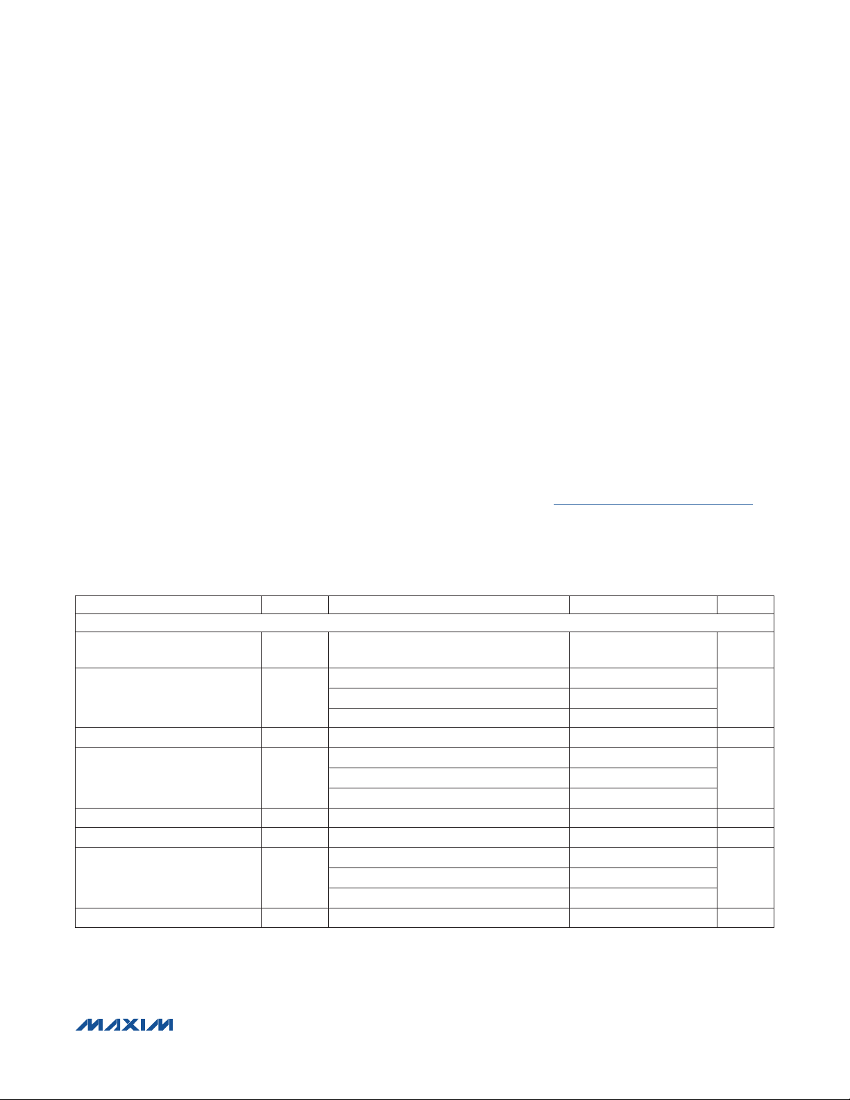
ELECTRICAL CHARACTERISTICS
(VDD = 3.3V, VSS = 0V, V
TA = +25NC, unless otherwise noted.) (Note 2)
PARAMETER SYMBOL CONDITIONS MIN TYP MAX UNITS
DC CHARACTERISTICS
Input Voltage Range V
Input Offset Voltage V
Input Offset Voltage Drift VOS - TC 0.8 5
Input Bias Current I
Input Capacitance C
Common-Mode Rejection Ratio CMRR VCM = -0.1V to (VDD + 0.1V) 75 90 dB
Open-Loop Gain A
Output Short-Circuit Current I
IN+
= V
= VDD/2, RL = 10kI to VDD/2, V
IN-
IN+ VIN-
OS
B
IN
OL
SC
Guaranteed by CMRR test -0.1
TA = +25NC
TA = -40°C to +125°C after calibration
TA = -40°C to +125°C
TA = +25NC
TA = -40NC to +85NC
TA = -40NC to +125NC
0.4V P V
0.4V P V
0.4V P V
To VDD or V
P VDD - 0.4V, R
OUT
P VDD - 0.4V, R
OUT
P VDD - 0.4V, R
OUT
SS
= VDD, TA = -40NC to +125NC. Typical values are at
SHDN
VDD
+ 0.1
10 50
100
500
0.01 0.5
10
100
0.4 pF
OUT
OUT
OUT
= 10kI
= 600I
= 32I
100 115
91 100
80
85 mA
V
FV
FV/NC
pA
dB
����������������������������������������������������������������� Maxim Integrated Products 2
Page 3
MAX44280
1.8V, 50MHz, Low-Offset,
Low-Power, Rail-to-Rail I/O Op Amp
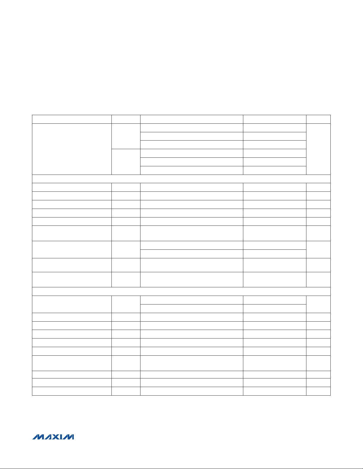
ELECTRICAL CHARACTERISTICS (continued)
(VDD = 3.3V, VSS = 0V, V
TA = +25NC, unless otherwise noted.) (Note 2)
PARAMETER SYMBOL CONDITIONS MIN TYP MAX UNITS
Output Voltage Swing
AC CHARACTERISTICS
Input Voltage-Noise Density e
Input Current-Noise Density i
Gain-Bandwidth Product GBWP 50 MHz
Minimum Stable Gain A
Slew Rate SR 30
Settling Time
Capacitive Load C
Total Harmonic Distortion THD
Output Transient Recovery Time
POWER-SUPPLY CHARACTERISTICS
Power-Supply Range V
Power-Supply Rejection Ratio PSRR VCM = VDD/2 82 95 dB
Quiescent Current I
Shutdown Supply Current
Shutdown Input Low V
Shutdown Input High V
Output Leakage Current in
Shutdown
Shutdown Input Bias Current IIL/I
Shutdown Turn-On Time
Turn-On Time t
Note 2: All devices are 100% production tested at TA = +25NC. Temperature limits are guaranteed by design.
IN+
= V
= VDD/2, RL = 10kI to VDD/2, V
IN-
R
= 10kI
VOL -
V
SS
VDD -
V
OH
n
n
MIN
LOAD
DD
DD
I
SHDN
IL
IH
I
SHDN
t
SHDN
ON
IH
OUT
R
= 600I
OUT
R
= 32I
OUT
R
= 10kI
OUT
R
= 600I
OUT
R
= 32I
OUT
f = 10kHz 12.7
f = 10kHz 1.2
V
= 2V
OUT
CL = 30pF (load), settle to 0.01%
No sustained oscillation, 5V/V 80
No sustained oscillation, 10V/V 500
f = 10kHz, VO = 2V
R
= 10kI
OUT
DV
OUT
RS = 20Ω, CL = 1nF (load)
Guaranteed by PSRR 1.8 5.5
TA = 0NC to +70NC
= VDD, TA = -40NC to +125NC. Typical values are at
SHDN
, VDD = 3.3V, AV = 5V/V,
P-P
, AV = 5V/V,
P-P
= 0.2V, VDD = 3.3V, AV = 5V/V;
20
50
400 700
10
40
400 800
nV/√Hz
fA/√Hz
5 V/V
0.6 µs
-110 dB
1 µs
1.7 5.5
750 1200 µA
1 µA
0.7 V
1.3 V
100 pA
1 µA
15 µs
10 ms
mV
V/Fs
pF
V
����������������������������������������������������������������� Maxim Integrated Products 3
Page 4
MAX44280
1.8V, 50MHz, Low-Offset,
Low-Power, Rail-to-Rail I/O Op Amp
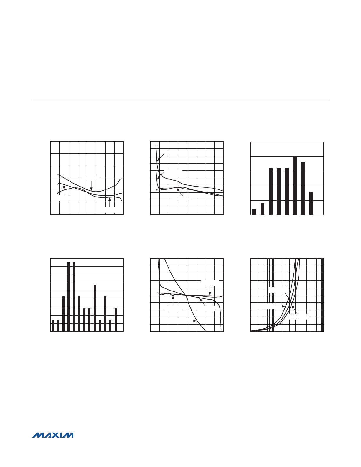
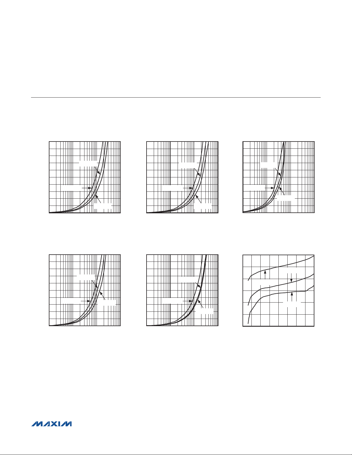
Typical Operating Characteristics
(VDD = 3.3V, VSS = 0V, V
IN+
= V
= VDD/2, RL = 10kI to VDD/2, V
IN-
= VDD, TA = -40NC to +125NC. Typical values are at
SHDN
TA = +25NC, unless otherwise noted. All devices are 100% production tested at TA = +25NC. Temperature limits are guaranteed by design.)
INPUT OFFSET VOLTAGE
vs. COMMON-MODE VOLTAGE
60
40
20
0
-20
INPUT OFFSET VOLTAGE (µV)
TA = +25°C
-40
-60
-0.5 3.5
COMMON-MODE VOLTAGE (V)
TA = -40°C
TA = +125°C
100
80
MAX44280 toc01
60
40
20
0
-20
-40
INPUT OFFSET VOLTAGE (µV)
-60
-80
3.02.52.01.51.00.50
-100
INPUT OFFSET VOLTAGE
vs. SUPPLY VOLTAGE
TA = -40°C
TA = +25°C
TA = +125°C
1.5 5.5
SUPPLY VOLTAGE (V)
5.04.53.5 4.02.5 3.02.0
25
MAX44280 toc02
20
15
10
PERCENT OCCURRENCE (%)
5
0
-15 -10 -5 051015 20 25
INPUT VOS HISTOGRAM
INPUT OFFSET VOLTAGE (µV)
OUTPUT VOLTAGE LOW
INPUT OFFSET DRIFT HISTOGRAM
18
16
14
12
10
8
6
PERCENT OCCURRENCE (%)
4
2
0
-2
-1.5
-1.8
-1.3-1-0.8
INPUT OFFSET DRIFT (µV/°C)
-0.5
-0.300.25
0.50
0.75
1.00
1.25
100
80
MAX44280 toc04
60
40
20
0
-20
-40
INPUT BIAS CURRENT (pA)
-60
-80
-100
-0.5 3.5
INPUT BIAS CURRENT
vs. COMMON-MODE VOLTAGE
TA = +25°C
TA = +85°CTA = -40°C
TA = +125°C
COMMON-MODE VOLTAGE (V)
200
180
MAX44280 toc05
160
140
120
100
80
60
OUTPUT VOLTAGE LOW (mV)
40
20
3.02.51.5 2.00.5 1.00
vs. OUTPUT SINK CURRENT
(VOL - VEE, VCC = 1.8V)
TA = +25°C
TA = +125°C
TA = -40°C
0
0.1 100
OUTPUT SINK CURRENT (mA)
101
MAX44280 toc03
MAX44280 toc06
����������������������������������������������������������������� Maxim Integrated Products 4
Page 5
MAX44280
1.8V, 50MHz, Low-Offset,
Low-Power, Rail-to-Rail I/O Op Amp
Typical Operating Characteristics (continued)
(VDD = 3.3V, VSS = 0V, V
IN+
= V
= VDD/2, RL = 10kI to VDD/2, V
IN-
= VDD, TA = -40NC to +125NC. Typical values are at
SHDN
TA = +25NC, unless otherwise noted. All devices are 100% production tested at TA = +25NC. Temperature limits are guaranteed by design.)
OUTPUT VOLTAGE LOW
vs. OUTPUT SINK CURRENT
(VOL - VEE, VCC = 3.3V)
200
180
160
140
120
100
80
60
OUTPUT VOLTAGE LOW (mV)
40
20
0
0.1 100
TA = +25°C
TA = +125°C
TA = -40°C
101
OUTPUT SINK CURRENT (mA)
OUTPUT VOLTAGE HIGH
vs. OUTPUT SOURCE CURRENT
(VCC - VOH, VCC = 3.3V)
200
180
160
140
120
100
80
60
OUTPUT VOLTAGE HIGH (mV)
40
20
0
0.1 100
OUTPUT SOURCE CURRENT (mA)
TA = +25°C
TA = +125°C
101
TA = -40°C
200
180
MAX44280 toc07
160
140
120
100
80
60
OUTPUT VOLTAGE LOW (mV)
40
20
0
200
180
MAX44280 toc10
160
140
120
100
80
60
OUTPUT VOLTAGE HIGH (mV)
40
20
0
OUTPUT VOLTAGE LOW
vs. OUTPUT SINK CURRENT
(VOL - VEE, VCC = 5V)
TA = +25°C
TA = +125°C
TA = -40°C
0.1 100
OUTPUT SINK CURRENT (mA)
101
OUTPUT VOLTAGE HIGH
vs. OUTPUT SOURCE CURRENT
(VCC - VOH, VCC = 5V)
TA = +25°C
TA = +125°C
TA = -40°C
0.1 100
OUTPUT SOURCE CURRENT (mA)
101
200
180
160
MAX44280 toc08
140
120
100
80
TA = +125°C
60
OUTPUT VOLTAGE HIGH (mV)
40
20
0
0.1 100
SUPPLY CURRENT vs. SUPPLY VOLTAGE
900
850
MAX44280 toc11
800
750
700
SUPPLY CURRENT (µA)
650
600
1.5 5.5
OUTPUT VOLTAGE HIGH
vs. OUTPUT SOURCE CURRENT
(VCC - VOH, VCC = 1.8V)
TA = +25°C
TA = -40°C
101
OUTPUT SOURCE CURRENT (mA)
TA = +25°C
TA = +125°C
TA = -40°C
5.04.54.03.53.02.52.0
SUPPLY VOLTAGE (V)
MAX44280 toc09
MAX44280 toc12
����������������������������������������������������������������� Maxim Integrated Products 5
Page 6

MAX44280
1.8V, 50MHz, Low-Offset,
Low-Power, Rail-to-Rail I/O Op Amp
Typical Operating Characteristics (continued)
(VDD = 3.3V, VSS = 0V, V
IN+
= V
= VDD/2, RL = 10kI to VDD/2, V
IN-
= VDD, TA = -40NC to +125NC. Typical values are at
SHDN
TA = +25NC, unless otherwise noted. All devices are 100% production tested at TA = +25NC. Temperature limits are guaranteed by design.)
SHUTDOWN SUPPLY CURRENT
vs. SUPPLY VOLTAGE
(V
= VEE)
1.0
0.9
0.8
0.7
0.6
0.5
0.4
0.3
0.2
SHUTDOWN SUPPLY CURRENT (µA)
0.1
0
SHDN
TA = +125°C
TA = -40°C
TA = +25°C
SUPPLY VOLTAGE (V)
POWER-SUPPLY REJECTION RATIO
vs. FREQUENCY
0
-20
-40
-60
PSRR (dB)
-80
-100
-120
0.01 100k
FREQUENCY (kHz)
5.04.54.03.53.02.52.01.5 5.5
10k1k1001010.1
140
120
MAX44280 toc13
100
80
60
OPEN-LOOP GAIN (dB)
40
20
-90
MAX44280 toc16
-92
-94
-96
REJECTION RATIO (dB)
-98
-100
OPEN-LOOP GAIN vs. FREQUENCY
0
0.01 100k
FREQUENCY (kHz)
10k1k1001010.1
DC CMRR AND PSRR
vs. TEMPERATURE
DC CMRR
DC PSRR
-50 125
TEMPERATURE (°C)
1007550250-25
MAX44280 toc14
MAX44280 toc17
COMMON-MODE REJECTION RATIO
vs. FREQUENCY
0
-20
-40
-60
CMRR (dB)
-80
-100
-120
FREQUENCY (kHz)
INPUT VOLTAGE-NOISE DENSITY
vs. FREQUENCY
500
450
400
350
300
250
200
150
100
50
INPUT-VOLTAGE NOISE DENSITY (nV/√Hz)
0
0.01 10k
FREQUENCY (kHz)
10k1k10010100.01 100k
1k1001010.1
MAX44280 toc15
MAX44280 toc18
����������������������������������������������������������������� Maxim Integrated Products 6
Page 7

MAX44280
11
1.8V, 50MHz, Low-Offset,
Low-Power, Rail-to-Rail I/O Op Amp
Typical Operating Characteristics (continued)
(VDD = 3.3V, VSS = 0V, V
IN+
= V
= VDD/2, RL = 10kI to VDD/2, V
IN-
= VDD, TA = -40NC to +125NC. Typical values are at
SHDN
TA = +25NC, unless otherwise noted. All devices are 100% production tested at TA = +25NC. Temperature limits are guaranteed by design.)
0.1Hz TO 10Hz OUTPUT-VOLTAGE NOISE
0.5µV/div
4s/div
MAX44280 toc19
TOTAL HARMONIC DISTORTION vs. FREQUENCY
= 2V
(V
-80
-85
-90
-95
-100
-105
-110
TOTAL HARMONIC DISTORTION (dB)
-115
-120
OUT
VCC = 3.3V
VCC = 5.5V
FREQUENCY (Hz)
P-P
)
100k10k10 100 1k
MAX44280 toc22
G
INPUT CURRENT-NOISE DENSITY
vs. FREQUENCY
5.0
4.5
4.0
3.5
3.0
2.5
2.0
1.5
1.0
INPUT-CURRENT NOISE DENSITY (fA/√Hz)
0.5
0
10 100k
FREQUENCY (Hz)
SMALL-SIGNAL TRANSIENT RESPONSE
= 5V/V, RF = 4kI, RG = 1kI)
(A
V
INPUT
20mV/div
VCC/2
OUTPUT
50mV/div
V
/2
CC
100ns/div
10k1000100
MAX44280 toc23
TOTAL HARMONIC DISTORTION vs. INPUT AMPLITUDE
= 5.5V, AV = 5V/V)
CC
OUTPUT AMPLITUDE (V)
4.54.00.5 1.0 1.5 2.5 3.02.0 3.5
MAX44280 toc20
(f = 10kHz, V
-80
-85
-90
-95
-100
THD (dB)
-105
-110
-115
-120
0 5.0
LARGE-SIGNAL TRANSIENT RESPONSE
= 5V/V, RF = 4kI, RG = 1kI)
(A
V
INPUT
100mV/div
OUTPUT
500mV/div
100ns/div
MAX44280 toc24
MAX44280 toc21
����������������������������������������������������������������� Maxim Integrated Products 7
Page 8
MAX44280
1.8V, 50MHz, Low-Offset,
Low-Power, Rail-to-Rail I/O Op Amp
Typical Operating Characteristics (continued)
(VDD = 3.3V, VSS = 0V, V
IN+
= V
= VDD/2, RL = 10kI to VDD/2, V
IN-
= VDD, TA = -40NC to +125NC. Typical values are at
SHDN
TA = +25NC, unless otherwise noted. All devices are 100% production tested at TA = +25NC. Temperature limits are guaranteed by design.)
PERCENT OVERSHOOT vs.
V
GND
CC
= 100mV
IN
10k1k
RESISTIVE LOAD (V
14
12
10
8
6
OVERSHOOT (%)
4
2
0
100 100k
RESISTANCE (I)
2V/div
)
P-P
MAX44280 toc25
POWER-UP TIME
STABILITY vs. CAPACITIVE LOAD AND
ISOLATION RESISTANCE
(R
IN SERIES C
60
50
40
30
20
ISOLATION RESISTANCE (Ω)
10
0
0 4000
MAX44280 toc28
LOAD
STABLE
UNSTABLE
GAIN = 10V/V
STABLE
UNSTABLE
CAPACITIVE LOAD (pF)
GAIN = 5V/V
LOAD
2V/div
)
100,000
MAX44280 toc26
10,000
1000
100
RESISTIVE LOAD (Ω)
10
350030002500200015001000500
TURN-ON TIME FROM SHUTDOWN
SHDN
V
SS
CAPACITIVE AND RESISTIVE LOAD
1
100 10,000
STABILITY vs.
(R
LOAD
UNSTABLE
STABLE
GAIN = 5V/V
CAPACITIVE LOAD (pF)
MAX44280 toc29
|| C
LOAD
GAIN = 10V/V
1000
)
UNSTABLE
STABLE
MAX44280 toc27
OUTPUT
500mV/div
GND
4ms/div
OUTPUT
500mV/div
V
SS
10µs/div
����������������������������������������������������������������� Maxim Integrated Products 8
Page 9

MAX44280
1.8V, 50MHz, Low-Offset,
Low-Power, Rail-to-Rail I/O Op Amp
Pin Configurations
TOP VIEW
+
IN+
1
VSS2
IN-
3
PIN NAME FUNCTION
1 IN+ Positive Input
2 V
3 IN- Negative Input
4 OUT Output
5
6 V
SS
SHDN
DD
MAX44280
SC70
Negative Power Supply. Bypass with a 0.1FF capacitor to ground.
Active-Low Shutdown
Positive Power Supply. Bypass with a 0.1FF capacitor to ground.
V
6
DD
5
SHDN
4
OUT
+
V
DD
654
MAX44280
123
IN+
(Ultra-Thin LGA)
SS
THIN µDFN
OUTSHDN
IN-V
Pin Description
����������������������������������������������������������������� Maxim Integrated Products 9
Page 10
MAX44280
1.8V, 50MHz, Low-Offset,
Low-Power, Rail-to-Rail I/O Op Amp
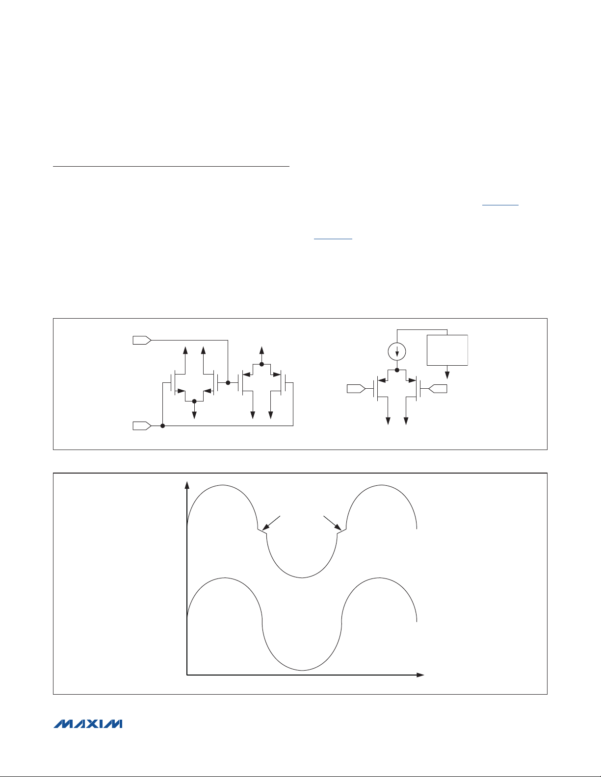
Detailed Description
The MAX44280 is a high-speed low-power op amp ideal
for signal processing applications due to the device’s
high precision and low-noise CMOS inputs. The device
self-calibrates on power-up to eliminate effects of temperature and power-supply variation.
The MAX44280 also features a low-power shutdown
mode that greatly reduces quiescent current while the
device is not operational and recovers in 30µs.
STANDARD INPUT STRUCTURE
Crossover Distortion
This op amp features a low-noise integrated charge
pump that creates an internal voltage rail 1V above
V
which is used to power the input differential
DD,
pair of pMOS transistors as shown in Figure 1. Such
a unique architecture eliminates crossover distortion common in traditional CMOS input architecture
(Figure 2), especially when used in a noninverting
configuration, such as for Sallen-Key filters.
The charge pump’s operating frequency lies well above
the unity-gain frequency of the amplifier. Thanks to its highfrequency operation and ultra-quiet circuitry, the charge
pump generates little noise, does not require external
components, and is entirely transparent to the user.
INTERNAL
CHARGE
PUMP
MAX44280 INPUTS STRUCTURE
Figure 1. Comparing the Input Structure of the MAX44280 to Standard Op-Amp Inputs
CROSSOVER
DISTORTION
AMPLIFIER OUTPUT
Figure 2. Crossover Distortion of Typical Amplifiers
���������������������������������������������������������������� Maxim Integrated Products 10
MAX44280
TIME
Page 11

MAX44280
1.8V, 50MHz, Low-Offset,
Low-Power, Rail-to-Rail I/O Op Amp
Applications Information
Power-Up Autotrim
The IC features an automatic trim that self-calibrates
the VOS of this device to less than 50FV of input offset
voltage on power-up. This self-calibration feature allows
the device to eliminate input offset voltage effects due
to power supply and operating temperature variation
simply by cycling its power. The autotrim sequence takes
approximately 10ms to complete and is triggered by an
internal power-on-reset (POR) circuitry. During this time,
the inputs and outputs are put into high impedance and
left unconnected.
Shutdown Operation
The MAX44280 features an active-low shutdown mode
that puts both inputs and outputs into high impedance
and substantially lowers the quiescent current to less
than 1FA. Putting the output into high impedance allows
multiple outputs to be multiplexed onto a single output
line without the additional external buffers. The device
does not self-calibrate when exiting shutdown mode
and retains its power-up trim settings. The device also
recovers from shutdown in under 30Fs.
The shutdown logic levels of the device is independent
of supply, allowing the shutdown feature of the device to
operate off of a 1.8V or 3.3V microcontroller, regardless
of supply voltage.
Rail-to-Rail Input/Output
The input voltage range of the IC extends 100mV above
V
and below VSS. The wide input common-mode
DD
voltage range allows the op amp to be used as a buffer and as a differential amplifier in a wide-variety of
signal processing applications. Output voltage high/low
is designed to be only 50mV above VSS and below VDD
allowing maximum dynamic range in single-supply applications. The high output current and capacitance drive
capability of the device make it ideal as an ADC driver
and a line driver.
Input Bias Current
The IC features a high-impedance CMOS input stage
and a specialized ESD structure that allows low-input
bias current operation at low-input, common-mode voltages. Low-input bias current is useful when interfacing
with high-ohmic sensors. It is also beneficial for designing transimpedance amplifiers for photodiode sensors.
This makes the device ideal for ground-referenced medical and industrial sensor applications.
Active Filters
The MAX44280 is ideal for a wide variety of active filter
circuits that makes use of the wide bandwidth, rail-to-rail
input/output stages and high-impedance CMOS inputs.
Driver for Interfacing with
the MAX11645 ADC
The IC’s tiny size and low noise make it a good fit for driving 12- to 16-bit resolution ADCs in space-constrained
applications. The Typical Application Circuit shows the
MAX44280 amplifier output connected to a lowpass filter
driving the MAX11645 ADC. The MAX11645 is part of a
family of 3V and 5V, 12-bit and 10-bit, 2-channel ADCs.
The MAX11645 offers sample rates up to 94ksps and
measures two single-ended inputs or one differential
input. These ADCs dissipate 670FA at the maximum sampling rate, but just 6FA at 1ksps and 0.5FA in shutdown.
Offered in the ultra-tiny, 1.9mm x 2.2mm WLP and FMAX8 packages, the MAX11645 ADCs are an ideal fit to pair
with the MAX44280 amplifier in portable applications.
Where higher resolution is required, refer to the MAX1069
(14-bit) and MAX1169 (16-bit) ADC families.
���������������������������������������������������������������� Maxim Integrated Products 11
Page 12
MAX44280
1.8V, 50MHz, Low-Offset,
Low-Power, Rail-to-Rail I/O Op Amp
PROCESS: BiCMOS
Chip Information
Ordering Information
PART TEMP RANGE PIN-PACKAGE
MAX44280AXT+ -40NC to +125NC 6 SC70 +AED
MAX44280AYT+ -40NC to +125NC
+Denotes a lead(Pb)-free/RoHS-compliant package.
6 Thin FDFN
(Ultra-Thin LGA)
TOP
MARK
+AZ
���������������������������������������������������������������� Maxim Integrated Products 12
Page 13
MAX44280
1.8V, 50MHz, Low-Offset,
Low-Power, Rail-to-Rail I/O Op Amp
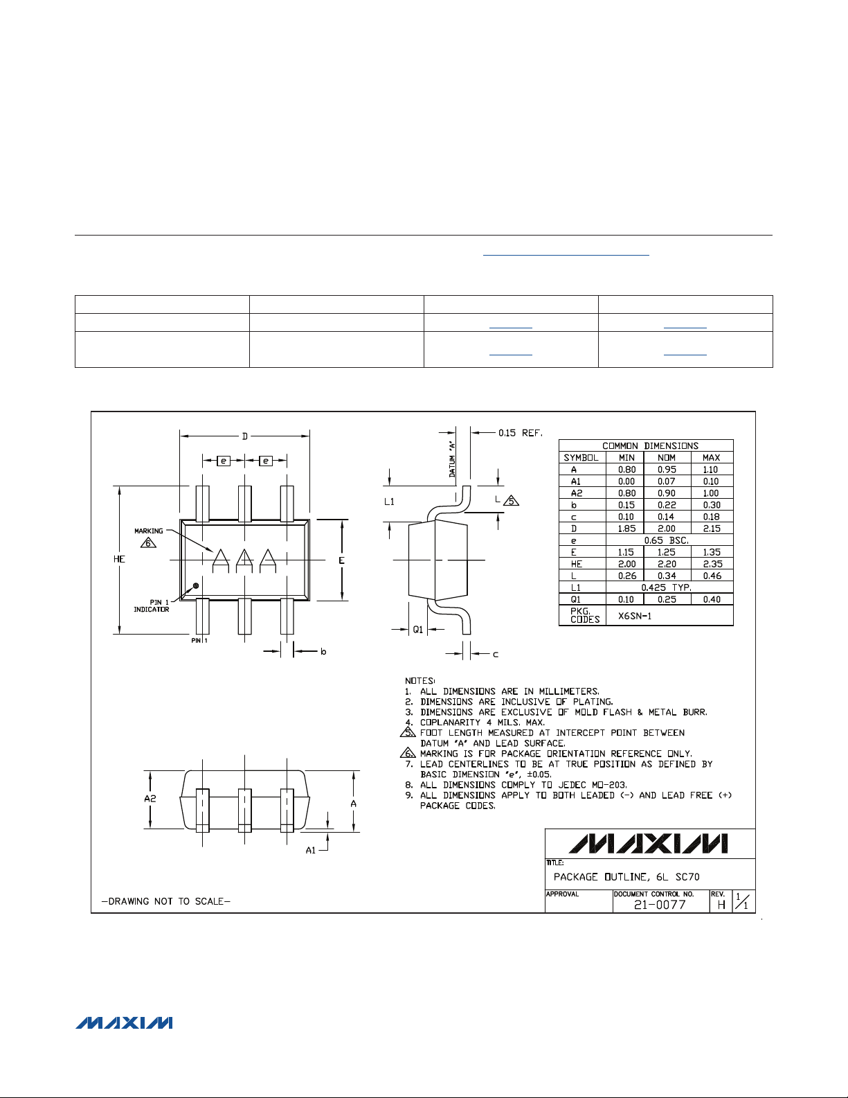
Package Information
For the latest package outline information and land patterns (footprints), go to www.maxim-ic.com/packages. Note that a “+”, “#”, or
“-” in the package code indicates RoHS status only. Package drawings may show a different suffix character, but the drawing pertains
to the package regardless of RoHS status.
PACKAGE TYPE PACKAGE CODE OUTLINE NO. LAND PATTERN NO.
6 SC70 X6SN+1
6 Thin FDFN
(Ultra-Thin LGA)
Y61A1+1
21-0077 90-0189
21-0190 90-0233
���������������������������������������������������������������� Maxim Integrated Products 13
Page 14

MAX44280
1.8V, 50MHz, Low-Offset,
Low-Power, Rail-to-Rail I/O Op Amp
Package Information (continued)
For the latest package outline information and land patterns (footprints), go to www.maxim-ic.com/packages. Note that a “+”, “#”, or
“-” in the package code indicates RoHS status only. Package drawings may show a different suffix character, but the drawing pertains
to the package regardless of RoHS status.
���������������������������������������������������������������� Maxim Integrated Products 14
Page 15

MAX44280
1.8V, 50MHz, Low-Offset,
Low-Power, Rail-to-Rail I/O Op Amp
Package Information (continued)
For the latest package outline information and land patterns (footprints), go to www.maxim-ic.com/packages. Note that a “+”, “#”, or
“-” in the package code indicates RoHS status only. Package drawings may show a different suffix character, but the drawing pertains
to the package regardless of RoHS status.
���������������������������������������������������������������� Maxim Integrated Products 15
Page 16

MAX44280
1.8V, 50MHz, Low-Offset,
Low-Power, Rail-to-Rail I/O Op Amp
Revision History
REVISION
NUMBER
0 12/11 Initial release —
1 4/12
REVISION
DATE
DESCRIPTION
Updated Package Thermal Characteristics, Electrical Characteristics, and Ordering
Information.
PAGES
CHANGED
2, 3, 12
Maxim cannot assume responsibility for use of any circuitry other than circuitry entirely embodied in a Maxim product. No circuit patent licenses are implied.
Maxim reserves the right to change the circuitry and specifications without notice at any time. The parametric values (min and max limits) shown in the Electrical
Characteristics table are guaranteed. Other parametric values quoted in this data sheet are provided for guidance.
Maxim Integrated Products, 120 San Gabriel Drive, Sunnyvale, CA 94086 408-737-7600 16
©
2012 Maxim Integrated Products Maxim is a registered trademark of Maxim Integrated Products, Inc.
 Loading...