

Page 1
EVALUATION KIT AVAILABLE
19-6144; Rev 0; 12/11
MAX44268
1.3mm x 1.3mm, Low-Power
Dual Comparator with Reference
General Description
The MAX44268 is an ultra-small and low-power dual
comparator ideal for battery-powered applications such
as cell phones, notebooks, and portable medical devices
that have extremely aggressive board space and power
constraints. The comparator is available in a miniature
1.3mm x 1.3mm, 9-bump WLP package, making it the
industry’s smallest dual comparator.
The IC can be powered from supply rails as low as 1.8V
and up to 5.5V. It also features a 1.236V ±1% reference
and a 0.7µA typical supply current per comparator. It has
a rail-to-rail input structure and a unique output stage that
limits supply current surges while switching. This design
also minimizes overall power consumption under dynamic conditions. The IC has open-drain outputs, making it
suitable for mixed voltage systems. The IC also features
internal filtering to provide high RF immunity. It operates
over a -40°C to +85°C temperature.
Applications
Smartphones
Notebooks
Two-Cell Battery-Powered Devices
Battery-Operated Sensors
Ultra-Low-Power Systems
Portable Medical Mobile Accessories
Features
S Ultra-Low Power Consumption
0.7µA per Comparator
S Ultra-Small 1.3mm x 1.3mm WLP Package
S Internal 1.236V ±1% Reference
S Guaranteed Operation Down to VCC = 1.8V
S Input Common-Mode Voltage Range Extends
200mV Beyond-the-Rails
S 6V Tolerant Inputs Independent of Supply
S Open-Drain Outputs
S Internal Filters Enhance RF Immunity
S Crowbar-Current-Free Switching
S Internal Hysteresis for Clean Switching
S No Output Phase Reversal for Overdriven Inputs
Ordering Information appears at end of data sheet.
For related parts and recommended products to use with this part,
refer to www.maxim-ic.com/MAX44268.related.
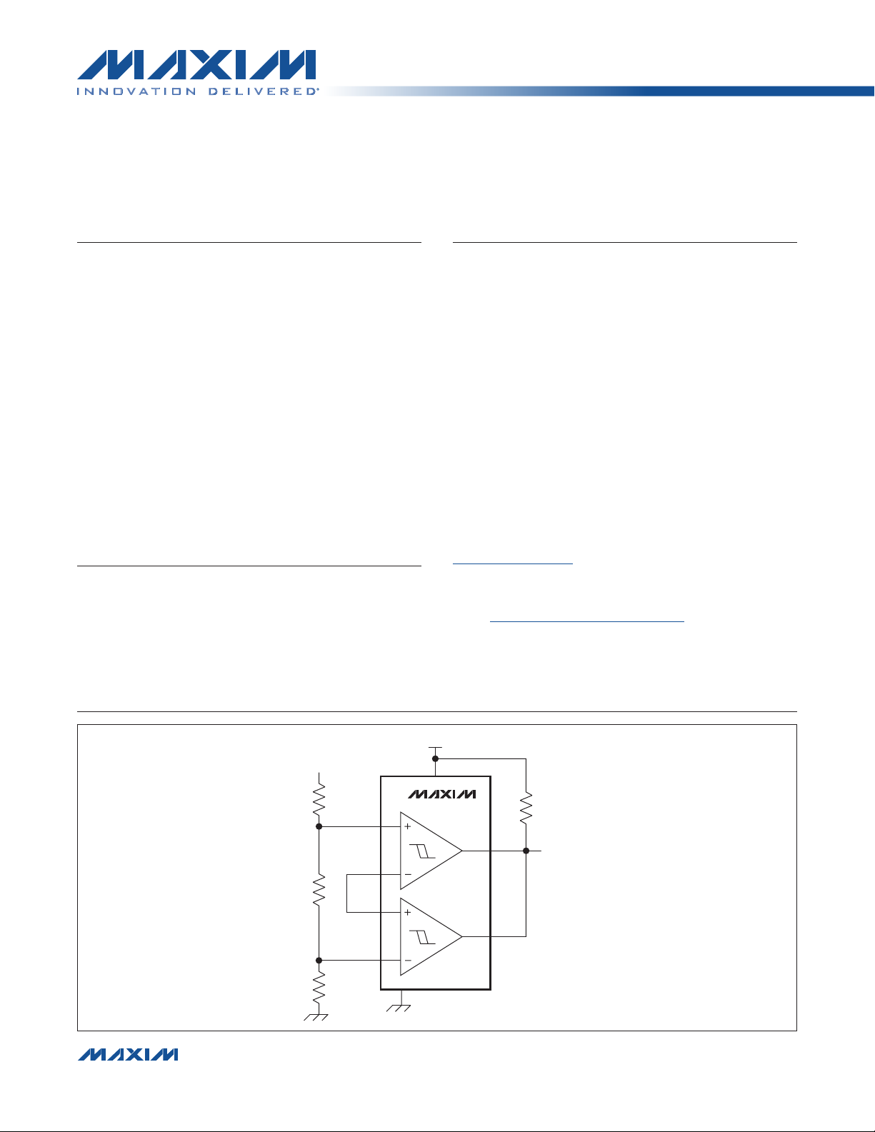
Typical Application Circuit
5V
V
IN
R3
INA+
REF/INA-
R2
INB+
INB-
R1
����������������������������������������������������������������� Maxim Integrated Products 1
MAX44268
GND
V
CC
OUTA
OUTB
POWERGOOD
For pricing, delivery, and ordering information, please contact Maxim Direct at 1-888-629-4642,
or visit Maxim’s website at www.maxim-ic.com.
Page 2
MAX44268
1.3mm x 1.3mm, Low-Power
Dual Comparator with Reference
ABSOLUTE MAXIMUM RATINGS
VCC to GND ............................................................. -0.3V to +6V
INA+, REF/INA-, INB+, INB- to GND ......................-0.3V to +6V
Output Voltage to GND (OUT_) ..............................-0.3V to +6V
Output Current (OUT_) .................................................... Q50mA
Output Short-Circuit Duration (OUT_) .......................Continuous
Continuous Power Dissipation (TA = +70NC)
WLP (derate 11.9mW/NC above TA = +70NC) .............952mW
PACKAGE THERMAL CHARACTERISTICS (Note 1)
WLP
Junction-to-Ambient Thermal Resistance (qJA) ..........84°C/W
Note 1: Package thermal resistances were obtained using the method described in JEDEC specification JESD51-7, using a four-
layer board. For detailed information on package thermal considerations, refer to www.maxim-ic.com/thermal-tutorial.
Stresses beyond those listed under “Absolute Maximum Ratings” may cause permanent damage to the device. These are stress ratings only, and functional operation of the device at these or any other conditions beyond those indicated in the operational sections of the specifications is not implied. Exposure to absolute
maximum rating conditions for extended periods may affect device reliability.
Continuous Input Current into Any Pin ............................ Q20mA
Operating Temperature Range .......................... -40NC to +85NC
Storage Temperature Range ............................ -65NC to +150NC
Junction Temperature .....................................................+150NC
Lead Temperature (soldering, 10s) ................................+300NC
Soldering Temperature (reflow) ......................................+260NC
ELECTRICAL CHARACTERISTICS
(VCC = 5V, V
unless otherwise noted.) (Note 2)
PARAMETER SYMBOL CONDITIONS MIN TYP MAX UNITS
DC CHARACTERISTICS
Input-Referred Hysteresis V
Input Offset Voltage V
Input Bias Current I
Output-Voltage Swing
Low
Input Voltage Range V
Output Short-Circuit
Current
Output Leakage Current I
GND
= 0V, V
IN-
= V
= 1.236V, R
IN+
HYS
OS
B
V
OL
CM
I
SC
LEAK
= 100kI to VCC, TA = -40NC to +85NC. Typical values are at TA = +25NC,
PULLUP
(V
- 0.2V) P VCM P (VCC + 0.2V) (Note 3)
GND
V
- 0.2V P VCM P
GND
VCC + 0.2V (Note 4)
TA = +25NC
TA = -40NC to +85NC
VCC = 1.8V,
I
= 1mA
SINK
VCC = 5V, I
6mA
Inferred from VOS test
Sinking, V
VCC = 5.5V, V
SINK
OUT
=
= V
OUT
TA = +25NC
-40NC P TA P +85NC
TA = +25NC
-40NC P TA P +85NC
TA = +25NC
-40NC P TA P +85NC
VCC = 1.8V 3
CC
VCC = 5V 30
= 5.5V 0.2 nA
V
GND
- 0.2V
4 6 mV
0.15 5
0.15
0.2
105 200
285 350
10
300
450
V
CC
+ 0.2V
mV
nA
mV
V
mA
����������������������������������������������������������������� Maxim Integrated Products 2
Page 3
MAX44268
1.3mm x 1.3mm, Low-Power
Dual Comparator with Reference
ELECTRICAL CHARACTERISTICS (continued)
(VCC = 5V, V
unless otherwise noted.) (Note 2)
PARAMETER SYMBOL CONDITIONS MIN TYP MAX UNITS
AC CHARACTERISTICS
Propagation Delay High
to Low (Note 5)
Propagation Delay Low to
High (Note 5)
Fall Time t
POWER SUPPLY
Supply Voltage Range V
Power-Supply Rejection
Ratio
Supply Current Per
Comparator
Power-Up Time t
Reference Voltage V
Reference Voltage
Temperature Coefficient
Reference Output Voltage
Noise
Reference Line
Regulation
Reference Load
Regulation
Note 2: All devices are 100% production tested at TA = +25NC. Temperature limits are guaranteed by design.
Note 3: Hysteresis is the input voltage difference between the two switching points.
Note 4: VOS is the average of the positive and negative trip points minus V
Note 5: Overdrive is defined as the voltage above or below the switching points.
GND
= 0V, V
IN-
= V
= 1.236V, R
IN+
Input overdrive = Q100mV, VCC = 5V
Input overdrive = Q100mV, VCC = 1.8V
t
PHL
t
PLH
F
CC
PSRR VCC = 1.8V to 5.5V 60 80 dB
I
CC
ON
REF
TC
VREF
e
N
δV
/δV
REF
δV
/δI
REF
Input overdrive = 100mV, VCC = 1.8V,
Comparator A
Input overdrive = Q20mV, VCC = 5V
Input overdrive = Q20mV, VCC = 1.8V
Input overdrive = Q100mV, VCC = 5V
Input overdrive = Q100mV, VCC = 1.8V
Input overdrive = Q20mV, VCC = 5V
Input overdrive = Q20mV, VCC = 1.8V
C
LOAD
Guaranteed from PSRR tests 1.8 5.5 V
VCC = 1.8V, TA = +25NC
VCC = 5V, -40NC P TA P +85NC
TA = +25NC, 1%
-40NC < TA < +85NC
TA = +25NC, 1%
10Hz to 1kHz, C
10Hz to 6kHz, C
CCVCC
0 < I
OUT
= 100kI to VCC, TA = -40NC to +85NC. Typical values are at TA = +25NC,
PULLUP
6
7
10
14
19
38
13
39
20
= 15pF 0.2
0.6 0.95
0.7 1.15
1 ms
1.224 1.236 1.248
1.205 1.267
40
= 1nF 75
REF
= 1nF 130
REF
= 1.8V to 5.5V 0.35 mV/V
< 100nA 0.05 mV/nA
OUT
.
REF
1.4
Fs
Fs
Fs
FAVCC = 5V, TA = +25NC
V
ppm/NC
FV
RMS
����������������������������������������������������������������� Maxim Integrated Products 3
Page 4
MAX44268
06
1.3mm x 1.3mm, Low-Power
Dual Comparator with Reference
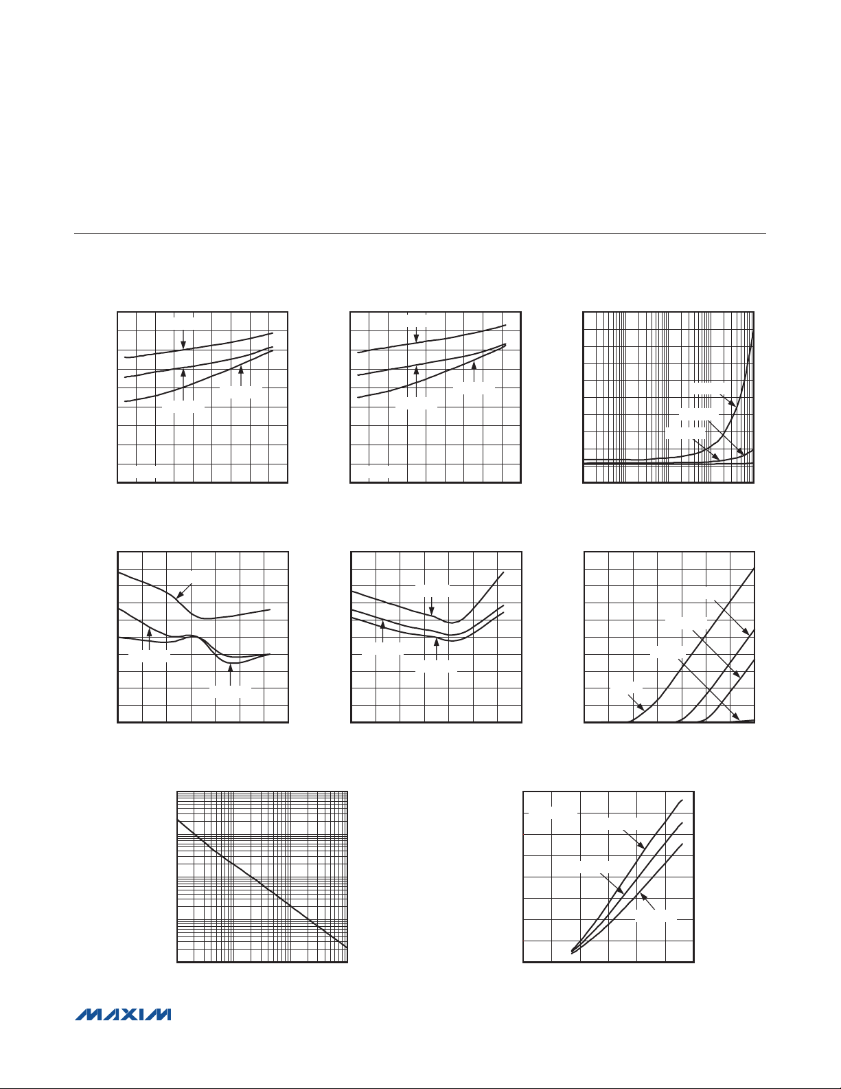
Typical Operating Characteristics
(VCC = 5V, V
GND
= 0V, V
IN-
= V
= 1.236V, R
IN+
= 100kΩ to VCC, TA = -40NC to +85NC. Typical values are at TA = +25NC, unless
PULLUP
otherwise noted. All devices are 100% production tested at TA = +25NC. Temperature limits are guaranteed by design.)
SUPPLY CURRENT vs. TRANSITION
SUPPLY CURRENT vs. SUPPLY VOLTAGE
1.8
1.6
1.4
1.2
1.0
0.8
0.6
SUPPLY CURRENT (µA)
0.4
0.2
0
1.5 6.0
V
= HIGH
OUT
TA = +85°C
TA = -40°C
TA = +25°C
SUPPLY VOLTAGE (V)
INPUT OFFSET VOLTAGE
vs. TEMPERATURE
0
-0.05
-0.10
-0.15
-0.20
-0.25
-0.30
VDD = 2.7V
-0.35
INPUT OFFSET VOLTAGE (mV)
-0.40
-0.45
-0.50
-40 100
VDD = 5V
VDD = 1.8V
TEMPERATURE (°C)
OUTPUT VOLTAGE LOW
vs. PULLUP RESISTANCE
10,000
)
EE
- V
1000
OL
100
10
OUTPUT VOLTAGE LOW (V
1
100 100k 54321
PULLUP RESISTANCE (I)
MAX44268 toc01
5.55.04.54.03.53.02.52.0
MAX44268 toc04
806020 400-20
10k1k
SUPPLY CURRENT vs. SUPPLY VOLTAGE
1.8
1.6
1.4
1.2
1.0
0.8
0.6
SUPPLY CURRENT (µA)
0.4
0.2
0
1.5 6.0
V
= LOW
OUT
TA = +85°C
TA = -40°C
TA = +25°C
SUPPLY VOLTAGE (V)
INPUT BIAS CURRENT
vs. TEMPERATURE
0.20
0.18
0.16
0.14
0.12
0.10
VDD = 2.7V
0.08
0.06
INPUT BIAS CURRENT (nA)
0.04
0.02
0
-40 100
MAX44268 toc07
VDD = 5V
VDD = 1.8V
TEMPERATURE (°C)
10
9
MAX44268 toc02
5.55.04.54.03.53.02.52.0
MAX44268 toc05
806020 400-20
8
7
6
5
4
SUPPLY CURRENT (µA)
3
2
1
0
1 10k
500
450
400
350
300
250
200
150
INPUT BIAS CURRENT (nA)
100
50
0
-1 6
SHORT-CIRCUIT CURRENT
vs. SUPPLY VOLTAGE
40
V
35
30
25
20
15
10
SHORT-CIRCUIT CURRENT (mA)
= LOW
OUT
TA = +25°C
5
0
SUPPLY VOLTAGE (V)
FREQUENCY (V
OVERDRIVE
VCC = 2.7V
VCC = 1.8V
INPUT FREQUENCY (Hz)
INPUT BIAS CURRENT
vs. COMMON-MODE VOLTAGE
VDD = 2.7V
VDD = 5V
VDD = 0V
INPUT COMMON-MODE VOLTAGE (V)
TA = -40°C
TA = +85°C
= 20mV)
VCC = 5V
1k10010
VDD = 1.8V
MAX44268 toc08
MAX44268 toc03
MAX44268 toc06
542 310
����������������������������������������������������������������� Maxim Integrated Products 4
Page 5
MAX44268
1.3mm x 1.3mm, Low-Power
Dual Comparator with Reference
Typical Operating Characteristics (continued)
(VCC = 5V, V
GND
= 0V, V
IN-
= V
= 1.236V, R
IN+
= 100kΩ to VCC, TA = -40NC to +85NC. Typical values are at TA = +25NC, unless
PULLUP
otherwise noted. All devices are 100% production tested at TA = +25NC. Temperature limits are guaranteed by design.)
PROPAGATION DELAY
INPUT OFFSET VOLTAGE HISTOGRAM
45
40
35
30
25
20
OCCURRENCE (%)
15
10
5
0
-2
INPUT OFFSET VOLTAGE (mV)
100
90
80
70
60
50
40
30
PROPAGATION DELAY (µs)
20
10
0
vs. INPUT OVERDRIVE (t
60
MAX44268 toc09
2.52.01.0 1.5-1.0 -0.5 0 0.5-1.5
PROPAGATION DELAY
vs. CAPACITIVE LOAD
t
PLH
t
PHL
CAPACITIVE LOAD (pF)
PROPAGATION DELAY
8006004002000 1000
PLH
LEAKAGE CURRENT vs. TEMPERATURE
0.50
0.45
0.40
0.35
0.30
0.25
VCC = 5V
0.20
0.15
0.10
OUTPUT LEAKAGE CURRENT (nA)
0.05
0
-50 110
MAX44268 toc12
VCC = 2.7V
TEMPERATURE (°C)
)
MAX44268 toc10
VCC = 1.8V
907030 50-10 10-30
PROPAGATION DELAY vs. TEMPERATURE
45
40
35
30
25
20
15
PROPAGATION DELAY (µs)
10
5
0
-40 100
12
vs. PULLUP RESISTANCE
120
100
80
60
40
PROPAGATION DELAY (µs)
20
0
(V
OVERDRIVE
= 100mV, VDD = 5V)
t
PLH
t
PHL
TEMPERATURE (°C)
PROPAGATION DELAY
vs. INPUT OVERDRIVE (t
100k
PULLUP RESISTANCE (I)
806020 400-20
)
PLH
t
PLH
t
PHL
1M10k1k
MAX44268 toc13
MAX44268 toc11
10M
50
TA = -40°C
40
30
20
PROPAGATION DELAY (µs)
10
0
0 1000
INPUT OVERDRIVE VOLTAGE (mV)
TA = +25°C
TA = +85°C
MAX44268 toc14
800600400200
10
8
6
4
PROPAGATION DELAY (µs)
2
0
TA = +85°C
0 1000
INPUT OVERDRIVE VOLTAGE (mV)
TA = -40°C
TA = +25°C
800600400200
����������������������������������������������������������������� Maxim Integrated Products 5
MAX44268 toc15
Page 6

MAX44268
1.3mm x 1.3mm, Low-Power
Dual Comparator with Reference
Typical Operating Characteristics (continued)
(VCC = 5V, V
GND
= 0V, V
IN-
= V
= 1.236V, R
IN+
= 100kΩ to VCC, TA = -40NC to +85NC. Typical values are at TA = +25NC, unless
PULLUP
otherwise noted. All devices are 100% production tested at TA = +25NC. Temperature limits are guaranteed by design.)
INPUT-REFERRED HYSTERESIS
vs. TEMPERATURE
4.5
4.0
3.5
3.0
2.5
2.0
1.5
1.0
INPUT-REFERRED HYSTERESIS (mV)
0.5
0
-40 100
TEMPERATURE (°C)
SMALL-SIGNAL TRANSIENT RESPONSE
50mV/div
SMALL-SIGNAL TRANSIENT RESPONSE
= 1.8V)
(V
CC
50mV/div
MAX44268 toc16
1V/div
806020 400-20
20µs/div
MAX44268 toc17
100mV/div
LARGE-SIGNAL TRANSIENT RESPONSE
= 5V)
(V
CC
MAX44268 toc19
200mV/div
LARGE-SIGNAL TRANSIENT RESPONSE
= 1.8V)
(V
CC
1V/div
20µs/div
= 5V)
(V
CC
MAX44268 toc20
MAX44268 toc18
2V/div
200mV/div
V
2V/div
V
OUT
2V/div
20µs/div
POWER-UP RESPONSE
V
IN
CC
800µs/div
MAX44268 toc21
2V/div
-0.3V TO +6V
V
OUT
NO OUTPUT PHASE REVERSAL
V
IN
20µs/div
MAX44268 toc22
20µs/div
����������������������������������������������������������������� Maxim Integrated Products 6
Page 7

MAX44268
1.3mm x 1.3mm, Low-Power
Dual Comparator with Reference
Typical Operating Characteristics (continued)
(VCC = 5V, V
GND
= 0V, V
IN-
= V
= 1.236V, R
IN+
= 100kΩ to VCC, TA = -40NC to +85NC. Typical values are at TA = +25NC, unless
PULLUP
otherwise noted. All devices are 100% production tested at TA = +25NC. Temperature limits are guaranteed by design.)
REF VOLTAGE vs. TEMPERATURE
1.240
1.239
1.238
1.237
1.236
1.235
1.234
REF VOLTAGE (V)
1.233
1.232
1.231
1.230
VCC = 1.8V
-60 100
TEMPERATURE (°C)
VCC = 2.7V
VCC = 5V
REF VOLTAGE vs. SUPPLY VOLTAGE
1.240
1.239
1.238
1.237
1.236
1.235
1.234
REF VOLTAGE (V)
1.233
1.232
1.231
1.230
1.5 5.5
SUPPLY VOLTAGE (V)
REF VOLTAGE vs. REF SOURCE CURRENT
AND TEMPERATURE
1.250
1.245
MAX44268 toc23
1.240
1.235
1.230
1.225
1.220
REF VOLTAGE (V)
1.215
1.210
1.205
806020 40-20 0-40
1.200
20 200
TA = +25°C
TA = +85°C
TA = -40°C
OUTPUT SOURCE CURRENT (nA)
MAX44268 toc24
180160120 14060 80 10040
REF VOLTAGE vs. REF SINK CURRENT
1.260
MAX44268 toc26
5.04.53.5 4.02.5 3.02.0
1.255
1.250
1.245
REF VOLTAGE (V)
1.240
1.235
1.230
REF VOLTAGE vs. REF SINK CURRENT
AND TEMPERATURE
1.280
1.275
1.270
1.265
1.260
1.255
1.250
REF VOLTAGE (V)
1.245
1.240
1.235
1.230
20 200
OUTPUT SINK CURRENT (nA)
VCC = 1.8V
VCC = 2.7V
VCC = 5V
OUTPUT SINK CURRENT (nA)
TA = +25°C
TA = +85°C
180160120 14060 80 1004020 200
TA = -40°C
MAX44268 toc25
180160120 14060 80 10040
MAX44268 toc27
REF VOLTAGE vs. REF SOURCE CURRENT
1.250
1.245
1.240
1.235
REF VOLTAGE (V)
1.230
1.225
1.220
VCC = 2.7V
VCC = 1.8V
VCC = 5V
OUTPUT SOURCE CURRENT (nA)
MAX44268 toc28
PERCENT OCCURRENCE (%)
180160120 14060 80 1004020 200
REF VOLTAGE DRIFT HISTOGRAM
18
16
14
12
10
8
6
4
2
0
1.230
1.232
1.234
1.231
1.233
1.235
REF VOLTAGE (V)
1.236 1.238 1.240
1.237
1.239
����������������������������������������������������������������� Maxim Integrated Products 7
MAX44268 toc29
Page 8

MAX44268
1.3mm x 1.3mm, Low-Power
Dual Comparator with Reference
Bump Configuration
TOP VIEW
MAX44268
1
+
REF/
A
INA-
B
GND N.C.
C
INB- INB+ OUTB
23
INA+ OUTA
V
CC
WLP
PIN NAME FUNCTION
A1 REF/INA- Reference Output/Comparator A Inverting Input
A2 INA+ Comparator A Noninverting Input
A3 OUTA Comparator A Output
B1 GND
B2 N.C. No Connection
B3 V
C1 INB- Comparator B Inverting Input
C2 INB+ Comparator B Noninverting Input
C3 OUTB Comparator B Output
CC
Negative Supply Voltage. Bypass to GND with a 1.0FF capacitor.
Positive Supply Voltage. Bypass to GND with a 1.0FF capacitor.
Bump Description
����������������������������������������������������������������� Maxim Integrated Products 8
Page 9

MAX44268
1.3mm x 1.3mm, Low-Power
Dual Comparator with Reference
Detailed Description
The MAX44268 is a general-purpose dual comparator for
battery-powered devices where area, power, and cost
constraints are crucial. The IC can operate with a low
1.8V supply rail typically consuming 0.7µA quiescent current per comparator. This makes it ideal for mobile and
very low-power applications. The IC’s common-mode
input voltage range extends 200mV beyond-the-rails. An
internal 4mV hysteresis ensures clean output switching,
even with slow-moving input signals.
Input Stage Structure
The input common-mode voltage range extends from
(V
- 0.2V) to (VCC + 0.2V). The comparator operates
GND
at any different input voltage within these limits with low
input bias current. Input bias current is typically 0.15nA if
the input voltage is between the supply rails. The device
also features a 1.236V reference voltage output on the
inverting input of comparator A.
The IC features a unique input ESD structure that can
handle voltages from -0.3V to +6V independent of supply
voltage. This allows for the device to be powered down
with a signal still present on the input without damaging the part. This feature is useful in applications where
one of the inputs has transient spikes that exceed the
supply rails.
No Output Phase Reversal
for Overdriven Inputs
The IC’s design is optimized to prevent output phase
reversal if both the inputs are within the input commonmode voltage range. If one of the inputs is outside the
input common-mode voltage range, then output phase
reversal does not occur as long as the other input is
kept within the valid input common-mode voltage range.
This behavior is shown in the No Output Phase Reversal
graph in the Typical Operating Characteristics section.
Open-Drain Output
The IC features an open-drain output, enabling greater
control of speed and power consumption in the circuit
design. The output logic level is also independent from
the input, allowing for simple level translation.
RF Immunity
The IC has very high RF immunity due to on-chip filtering
of RF sensitive nodes. This allows the IC to hold its output
state even in the presence of high amounts of RF noise.
This improved RF immunity makes the IC ideal for mobile
wireless devices.
Applications Information
Hysteresis
Many comparators oscillate in the linear region of operation because of noise or undesired parasitic feedback.
This tends to occur when the voltage on one input is
equal or very close to the voltage on the other input.
The hysteresis in a comparator creates two trip points:
one for the rising input voltage and one for the falling input
voltage (Figure 1). The difference between the trip points
is the hysteresis. When the comparator’s input voltages
are equal and the output trips, the hysteresis effectively
causes one comparator input to move quickly past the
other. This takes the input out of the region where oscillation occurs. This provides clean output transitions for
noisy, slow-moving input signals. The IC has an internal
hysteresis of 4mV. Additional hysteresis can be generated with three resistors using positive feedback (Figure 2).
IN+
IN-
V
HYST
OUT
Figure 1. Threshold Hysteresis Band (Not to Scale)
R2
V
IN
R4
Figure 2. Adding Hysteresis with External Resistors
THERSHOLDS
HYSTERESIS BAND
R3
V
REF
V
CC
MAX44268
GND
OUT
V
TH
V
TL
R1
����������������������������������������������������������������� Maxim Integrated Products 9
Page 10

MAX44268
1.3mm x 1.3mm, Low-Power
Dual Comparator with Reference
Use the following procedure to calculate resistor values.
1) Select R3. Input bias current at IN_+ is less than
15nA. To minimize errors caused by the input bias
current, the current through R3 should be at least
1.5µA. Current through R3 at the trip point is (V
V
)/R3. Considering the two possible output states
OUT
REF
-
in solving for R3 yields two formulas:
R3 = V
/IR3 and R3 = [(VCC - V
REF
)/IR3] - R1
REF
Use the smaller of the two resulting resistor values.
For example, for VCC = 5V, IR3 = -1.5µA, R1 =
200kI, and a V
= 1.236V, the two resistor values
REF
are 827kI and 1.5MI. Therefore, for R3 choose the
standard value of 825kI.
2) Choose the hysteresis band required (VHB). In this
example, the VHB = 50mV.
3) Calculate R2 according to the following equation:
V
= +
R2 (R1 R3 )
V
CC
HB
+
(V
REF
x R1) R 3
For this example, insert the value:
50mV
R2 (200k 0.825M ) 9.67k
= Ω+ Ω = Ω
5.3
For this example, choose standard value R2 = 9.76kI.
4) Choose the trip point for VIN rising (V
) in such a
THR
way that:
V
V V1
>+
THR REF
V
is the threshold voltage at which the com-
THR
parator switches its output from low to high, as V
HB
V
CC
IN
rises above the trip point. For this example, choose
V
= 3V.
THR
5) Calculate R4 as follows:
=
R4
V
THR
V
REF
= = Ω
R4 6.93k
3 11
1.236V x 9.76 9.76 825
1
11
--
x R2 R2 R3
1
--
For this example, choose a standard value of 6.98kI.
6) Verify the trip voltages and hysteresis as follows:
111
= ++
VV
THR REF
= ++
VV
THF REF
xR2
R2 R3 R4
111
x R2
R2 R1 R3 R4
R2
-x
R1 R3
+
+
V
CC
The hysteresis network in Figure 2 can be simplified if the
reference voltage is chosen to be at midrail and the trip
points of the comparator are chosen to be symmetrical
about the reference voltage. Use the circuit in Figure 3
if the reference voltage can be designed to be at the
center of the hysteresis band. For the symmetrical case,
follow the same steps outlined in the paragraph above
to calculate the resistor values except that in this case,
resistor R4 approaches infinity (open). So in the previous example, using comparator B with V
V
= 2.525V and V
THR
= 2.475V then using the above
THF
REF
= 2.5V, if
formulas, results in R1 = 200kI, R2 = 9.09kI, and R3 =
825kI, R4 = not installed.
Logic-Level Translator
Due to the open-drain output of the IC, the device can
translate between two different logic levels (Figure 4). If
the internal 4mV hysteresis is not sufficient, then external
resistors can be added to increase the hysteresis as
shown in Figure 2 and Figure 3.
V
CC
R3
REF
R1
is at
R2
V
IN
V
REF
Figure 3. Simplified External Hysteresis Network if V
the Center of the Hysteresis Band
MAX44268
OUT
GND
���������������������������������������������������������������� Maxim Integrated Products 10
Page 11

MAX44268
1.3mm x 1.3mm, Low-Power
Dual Comparator with Reference
Power-On-Reset Circuit
The IC can be used to make a power-on-reset circuit as
displayed in Figure 5. The negative input provides the
ratiometric reference with respect to the power supply
and is created by a simple resistive divider. Choose
reasonably large values to minimize the power consumption in the resistive divider. The positive input provides
the power-on delay time set by the time constant of the
RC circuit formed by R2 and C1. This simple circuit can
be used to power up the system in a known state after
ensuring that the power supply is stable. Diode D1 provides a rapid reset in the event of unexpected power loss.
If using comparator A, R3 and R4 are not populated and
REF settles in approximately 100µs.
Relaxation Oscillator
The IC can also be used to make a simple relaxation
oscillator (Figure 6) using comparator B. By adding the
RC circuit R5 and C1, a standard Schmidt Trigger circuit
referenced to a set voltage is converted into an astable
V
CC
V
PULL
MAX44268
V
IN
V
REF
R1
OUT
multivibrator. As shown in Figure 7, IN- is a sawtooth
waveform with capacitor C1 alternately charging and
discharging through resistor R5. The external hysteresis
network formed by R1 to R4 defines the trip voltages as:
R3 x R4
R2R3 R2R4 R3R4
++
R4R5(R1 R2 R3)
R1R 3 R 4
+
++
++ +
R2(R1R3 R3R5 R1R5)
V
T_FALL
V
T_RISE
V
=
CC
V
=
CC
R4R5 (R1 R2 R3) R1R3R4
+ ++
Using the basic time domain equations for the charging
and discharging of an RC circuit, the logic-high time,
logic-low time, and frequency can be calculated as:
V
t
LOW
R5C1 ln
=
T_FALL
V
T_RISE
Since the comparator’s output is open drain, it goes to
high impedance corresponding to logic-high. So, when
the output is at logic-high, the C1 capacitor charges
through the resistor network formed by R1 to R5. An
accurate calculation of t
would have involved
HIGH
applying thevenin’s theorem to compute the equivalent
thevenin voltage (V
THEVENIN
) and thevenin resistance
GND
Figure 4. Logic-Level Translator
V
CC
R2D1
R3
R4
C1
Figure 5. Power-On Reset Circuit
���������������������������������������������������������������� Maxim Integrated Products 11
V
CC
MAX44268
GND
RESET
V
CC
R3
V
CC
R2
R1
Figure 6. Relaxation Oscillator
R4
C1
MAX44268
OUT
GND
R5
R1
Page 12

MAX44268
11
+
1.3mm x 1.3mm, Low-Power
Dual Comparator with Reference
(R
THEVENIN
) in series with the capacitor C1. t
HIGH
can
then be computed using the basic time domain equations for the charging RC circuit as:
The t
V-
HIGH
V
HIGH
THEVENIN
R (R2 R4) R3 R1 R5
THEVENIN
THEVENIN
= ++
[ ]
V (R2 R4) R3
[ ]
CC
= +
(R2 R4) R3 R1 R2 R4
x
(R2 R4) R3 R1
calculation can be simplified by selecting the
R C1 ln
=
t
THEVENIN
V-
THEVENIN
+
++ +
R1
++
V
T_RISE
V
T_FALL
V x R4
CC
component values in such a way that R3 >> R1 and R5
>> R1. This ensures that the output of the comparator
goes close to VCC when at logic-high (that is, V
~ VCC and R
THEVENIN
~ R5). With this selection, t
THEVENIN
HIGH
can be approximated as:
V-
V
T_RISE
t
HIGH
R5C1 ln
=
CC
V-
V
CC
T_FALL
The frequency of the relaxation oscillator is:
Window Detector Circuit
The IC is ideal for window detectors (undervoltage/overvoltage detectors). Typical Application Circuit shows a
simple window detector circuit. By changing the values
of R1, R2, and R3 different voltage threshold values can
be chosen. For this example, assume a single-cell Li+
battery with a 2.9V end-of-life charge, a peak charge of
4.2V, and a nominal value of 3.6V. OUTA provides an
active-low undervoltage indication, and OUTB provides
an active-low overvoltage indication. The open-drain outputs of both the comparators are wired ORed to give an
active-high power-good signal.
The design procedure is as follows:
1) Select R1. The input bias current into INB- is less than
15nA, so the current through R1 should exceed 1.5µA
for the thresholds to be accurate. In this example,
choose R1 = 825kI (1.236V/1.5µA).
2) Calculate R2 + R3. The overvoltage threshold should
be 4.2V when VIN is rising. The design equation is as
follows:
V
+=
R2 R3 R1 x - 1
=
825 x -1
=1969k
OTH
V
REF
4.2
1.236
Ω
f
= =
tt
HIGH LOW
V
T_FALL
C1 WAVEFORM
V
T_RISE
OUT
WAVEFORM
Figure 7. Relaxation Oscillator Waveforms
R 5 C1 1n
���������������������������������������������������������������� Maxim Integrated Products 12
V
T_FALL
V
T_RISE
V -V
( )
CC T_RISE
V-
( )
V
T_FALL
CC
3) Calculate R2. The undervoltage threshold should be
2.9V when VIN is falling. The design equation is as
follows:
V
R2 (R1 R2 R3)x - R1
=++
825 1969 x 1.236/2.9 - 825
= +
( ) ( )
( )
370k
= Ω
REF
V
UTH
For this example, choose a 374kI standard value 1%
resistor.
4) Calculate R3:
R3 (R2 R3) - R2
= +
1969k - 374k
=ΩΩ
=1.595M
Ω
For this example, choose a 1.58MI standard value 1%
resistor.
Page 13

1.3mm x 1.3mm, Low-Power
Dual Comparator with Reference
Board Layout and Bypassing
Use 1.0FF bypass capacitors from VCC to GND. To maximize performance, minimize stray inductance by putting
this capacitor close to the VCC pin and reducing trace
lengths. Use 1nF bypass capacitors from REF/INA- to
GND as close as possible to the IC. Do not route noisy
traces near REF/INA-.
Jack Detect
The IC can be used to detect peripheral devices
connected to a circuit using comparator B. This includes
a simple jack-detect scheme for cell phone applications. Figure 8 shows how the device can be used in
conjunction with an external reference to detect an
accessory ID input. The open-drain output of
the devices allows the output logic level to be controlled independent of the peripheral device’s
making interfacing and controlling external devices
as simple as monitoring a few digital inputs on a
microcontroller or codec.
load,
V
CC
V
REF
V
200kI
CONNECTOR
ACCESSORY
ID
Figure 8. Jack Detector Circuit
MAX44268
MAX44268
CC
GND
OUT2
V
PULL
PROCESS: BiCMOS
Chip Information
Ordering Information
PART TEMP RANGE
MAX44268EWL+T
+Denotes a lead(Pb)-free/RoHS-compliant package.
T = Tape and reel.
-40NC to +85NC
PIN-
PACKAGE
9 WLP +AJK
TOP
MARK
���������������������������������������������������������������� Maxim Integrated Products 13
Page 14

MAX44268
1.3mm x 1.3mm, Low-Power
Dual Comparator with Reference
Package Information
For the latest package outline information and land patterns (footprints), go to www.maxim-ic.com/packages. Note that a “+”, “#”, or
“-” in the package code indicates RoHS status only. Package drawings may show a different suffix character, but the drawing pertains
to the package regardless of RoHS status.
PACKAGE TYPE PACKAGE CODE OUTLINE NO. LAND PATTERN NO.
9 WLP W91B1-6
21-0430
Refer to Application Note 1891
���������������������������������������������������������������� Maxim Integrated Products 14
Page 15

MAX44268
1.3mm x 1.3mm, Low-Power
Dual Comparator with Reference
Revision History
REVISION
NUMBER
0 12/11 Initial release —
REVISION
DATE
DESCRIPTION
PAGES
CHANGED
Maxim cannot assume responsibility for use of any circuitry other than circuitry entirely embodied in a Maxim product. No circuit patent licenses are implied.
Maxim reserves the right to change the circuitry and specifications without notice at any time. The parametric values (min and max limits) shown in the Electrical
Characteristics table are guaranteed. Other parametric values quoted in this data sheet are provided for guidance.
Maxim Integrated Products, 120 San Gabriel Drive, Sunnyvale, CA 94086 408-737-7600 15
©
2011 Maxim Integrated Products Maxim is a registered trademark of Maxim Integrated Products, Inc.
 Loading...