

19-1831; Rev 1; 1/09
Low-Cost, Low-Power, Ultra-Small, 3V/5V, 500MHz
Single-Supply Op Amps with Rail-to-Rail Outputs
General Description
The MAX4412 single and MAX4413 dual operational
amplifiers are unity-gain-stable devices that combine
high-speed performance, low supply current, and ultrasmall packaging. Both devices operate from a single
+2.7V to +5.5V supply, have rail-to-rail outputs, and
exhibit a common-mode input voltage range that
extends from 100mV below ground to within +1.5V of
the positive supply rail.
The MAX4412/MAX4413 achieve a 500MHz -3dB bandwidth and a 140V/µs slew rate while consuming only
1.7mA of supply current per amplifier. This makes the
MAX4412/MAX4413 ideal for low-power/low-voltage,
high-speed portable applications such as video, communications, and instrumentation.
For systems requiring tighter specifications, Maxim
offers the MAX4414–MAX4419 family of operational
amplifiers. The MAX4414–MAX4419 are laser trimmed
versions of the MAX4412/MAX4413 and include compensated and uncompensated devices.
The MAX4412 is available in ultra-small 5-pin SC70 and
SOT23 packages, while the MAX4413 is available in a
space-saving 8-pin SOT23.
________________________Applications
Battery-Powered Instruments
Portable Communications
Keyless Entry Systems
Cellular Telephones
Video Line Drivers
Baseband Applications
Features
♦ Ultra-Low 1.7mA Supply Current
♦ Low Cost
♦ Single +3V/+5V Operation
♦ High Speed
500MHz -3dB Bandwidth
50MHz 0.1dB Gain Flatness
140V/µs Slew Rate
♦ Rail-to-Rail Outputs
♦ Input Common-Mode Range Extends Beyond V
♦ Low Differential Gain/Phase: 0.01%/0.03°
♦ Low Distortion at 5MHz
-93dBc SFDR
0.003% Total Harmonic Distortion
♦ Ultra-Small SC70 and SOT23 Packages
Ordering Information
PART TEMP RANGE
MAX4412EXK-T -40°C to +85°C
MAX4412EUK-T -40°C to +85°C
MAX4413EKA-T -40°C to +85°C
-Denotes a package containing lead(Pb).
T = Tape and reel.
PIN-
PACKAGE
5 SC70
5 SOT23
8 SOT23
TOP
M ARK
ABH
ADOL
AADR
MAX4412/MAX4413
EE
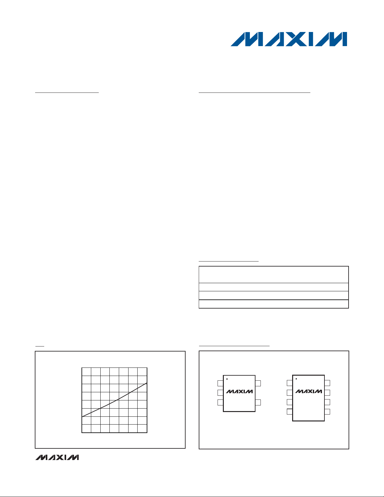
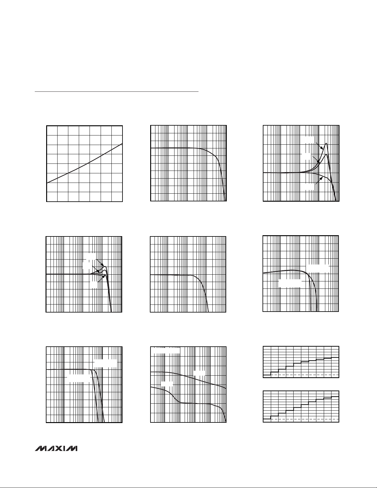
Typical Operating Characteristic
SUPPLY CURRENT vs.
SUPPLY VOLTAGE (PER AMPLIFER)
2.0
1.9
1.8
1.7
1.6
1.5
SUPPLY CURRENT (mA)
1.4
1.3
1.2
2.7 3.5 3.93.1
SUPPLY VOLTAGE (V)
________________________________________________________________
4.3
4.7 5.1 5.5
MAX4412 toc01
TOP VIEW
1
OUT
V
2
EE
IN+
MAX4412
34
SC70/SOT23
Pin Configurations
1
5 V
OUTA
CC
2
MAX4413
3
INA+
IN-
4
EE
SOT23
Maxim Integrated Products
87V
6
5
CC
OUTBINA-
INB-
INB+V
1
For pricing, delivery, and ordering information, please contact Maxim Direct at 1-888-629-4642,
or visit Maxim's website at www.maxim-ic.com.
MAX4412/MAX4413
Low-Cost, Low-Power, Ultra-Small, 3V/5V, 500MHz
Single-Supply Op Amps with Rail-to-Rail Outputs
2 _______________________________________________________________________________________
ABSOLUTE MAXIMUM RATINGS
DC ELECTRICAL CHARACTERISTICS
(VCC= +2.7V to +5.5V, VCM= VCC/2 - 0.75V, VEE= 0, RL= ∞ to VCC/2, V
OUT
= VCC/2, TA= T
MIN
to T
MAX
, unless otherwise noted.
Typical values are at T
A
= +25°C.) (Note 1)
Stresses beyond those listed under “Absolute Maximum Ratings” may cause permanent damage to the device. These are stress ratings only, and functional
operation of the device at these or any other conditions beyond those indicated in the operational sections of the specifications is not implied. Exposure to
absolute maximum rating conditions for extended periods may affect device reliability.
Supply Voltage (VCCto VEE)..................................................+6V
Differential Input Voltage ....................................................±2.5V
IN_-, IN_+, OUT_..............................(V
CC
+ 0.3V) to (VEE- 0.3V)
Current into Input Pins ......................................................±20mA
Output Short-Circuit Duration to V
CC
or VEE..............Continuous
Continuous Power Dissipation (T
A
= +70°C)
5-Pin SC70 (derate 3.1mW/°C above +70°C)..............247mW
5-Pin SOT23 (derate 7.1mW/°C above +70°C)............571mW
8-Pin SOT23 (derate 9.1mW/°C above +70°C)............727mW
Operating Temperature Range ...........................-40°C to +85°C
Junction Temperature......................................................+150°C
Storage Temperature Range .............................-65°C to +150°C
Lead Temperature (soldering, 10s) .................................+300°C
PARAMETER SYMBOL CONDITIONS MIN TYP MAX UNITS
Operating Supply Voltage Range V
Quiescent Supply Current
(per amplifier)
Input Common Mode Voltage
Range
Input Offset Voltage V
Input Offset Voltage Temperature
Coefficient
Input Offset Voltage Matching MAX4413 ±1mV
Input Bias Current I
Input Offset Current I
Input Resistance R
Common Mode Rejection Ratio CMRR VEE - 0.1V < VCM < VCC - 1.5V 60 94 dB
Open-Loop Gain A
TC
V
S
I
S
CM
OS
VOS
B
OS
IN
VOL
Guaranteed by PSRR test 2.7 5.5 V
VCC = +5V 1.7 3.5
VCC = +3V 1.5
Guaranteed by CMRR test
Differential mode,
-0.04V ≤ (V
Common mode,
V
EE
VCC = +5V
VCC = +3V
IN+
- 0.1V < VCM < VCC - 1.5V
- V
IN-)
+0.2V ≤ V
R
+0.4V ≤ V
R
+1V ≤ V
R
+0.2V ≤ V
R
+0.25V ≤ V
R
+0.5V ≤ V
R
≤ +0.04V
= 10kΩ
L
= 1kΩ
L
= 150Ω
L
= 10kΩ
L
= 1kΩ
L
= 150Ω
L
≤ +4.8V,
OUT
≤ +4.6V,
OUT
≤ +4V,
OUT
≤ +2.8V,
OUT
≤ +2.75V
OUT
≤ +2.5V,
OUT
V
EE
0.1
78 93
68 80
-
0.4 9 mV
1.6 4 μA
0.1 0.7 μA
VCC -
1.5
3 μV/°C
60 kΩ
16 MΩ
65
90
78
62
mA
V
dB
MAX4412/MAX4413
Low-Cost, Low-Power, Ultra-Small, 3V/5V, 500MHz
Single-Supply Op Amps with Rail-to-Rail Outputs
_______________________________________________________________________________________ 3
AC ELECTRICAL CHARACTERISTICS
(VCC= +5V, VEE= 0, VCM= +1.75V, RL= 1kΩ connected to VCC/2, CL= 5pF, A
VCL
= +1V/V, TA= +25°C, unless otherwise noted.)
DC ELECTRICAL CHARACTERISTICS (continued)
(VCC= +2.7V to +5.5V, VCM= VCC/2 - 0.75V, VEE= 0, RL= ∞ to VCC/2, V
OUT
= VCC/2, TA= T
MIN
to T
MAX
, unless otherwise noted.
Typical values are at T
A
= +25°C.) (Note 1)
PARAMETER SYMBOL CONDITIONS MIN TYP MAX UNITS
VCC = +5V
Output Voltage Swing V
OUT
VCC = +3V
Output Current I
Output Short-Circuit Current I
OUT
SC
RL = 20Ω connected to V
Sinking or sourcing ±85 mA
Power Supply Rejection Ratio PSRR VCC = +2.7V to +5.5V, VCM = 0, V
RL = 10kΩ
RL = 1kΩ
R
=
L
150Ω
RL = 10kΩ
RL = 1kΩ
R
=
L
150Ω
or V
C C
VCC - V
OH
- V
V
OL
EE
VCC - V
OH
- V
V
OL
EE
VCC - V
OH
V
- V
OL
EE
VCC - V
OH
- V
V
OL
EE
VCC - V
OH
- V
V
OL
EE
VCC - V
OH
V
- V
OL
EE
, V
= + 5V ±25 ±75 mA
E E
C C
= 2V 60 77 dB
OUT
0.085
0.015
0.105 0.275
0.035 0.125
0.385
0.150
0.06
0.01
0.075
0.025
0.275
0.070
V
Small Signal -3dB Bandwidth BW
Large Signal -3dB Bandwidth BW
Bandwidth for 0.1dB Flatness BW
Slew Rate SR V
Rise/Fall Time t
Settling Time to 0.1% t
Spurious-Free Dynamic Range SFDR
PARAMETER SYMBOL CONDITIONS MIN TYP MAX UNITS
V
SS
LS
0.1dB
t
R,
S 1%
F
= 100mV p - p 500 MHz
OU T
V
= 2Vp-p 30 MHz
OUT
V
= 100mVp-p 50
OUT
V
= 2Vp-p 16
OUT
= 2V step 140 V/µs
OUT
V
= 2V step, 10% to 90% 14 ns
OUT
V
= 2V step 100 ns
OUT
VCC = +5V, fC = 5MHz, V
= +3V, fC = 5MHz, V
V
CC
OUT
OUT
= 1Vp-p -84
= 1Vp-p -93
MHz
dBc
MAX4412/MAX4413
Low-Cost, Low-Power, Ultra-Small, 3V/5V, 500MHz
Single-Supply Op Amps with Rail-to-Rail Outputs
4 _______________________________________________________________________________________
Note 1: All devices are 100% production tested at TA= +25°C. Specifications over temperature are guaranteed by design.
Note 2: Guaranteed by design.
AC ELECTRICAL CHARACTERISTICS (continued)
(VCC= +5V, VEE= 0, VCM= +1.75V, RL= 1kΩ connected to VCC/2, CL= 5pF, A
VCL
= +1V/V, TA= +25°C, unless otherwise noted.)
2nd Harmonic Distortion
3rd Harmonic Distortion
Total Harmonic Distortion THD
Two-Tone, Third-Order
Intermodulation Distortion
Differential Gain Error DG RL = 150Ω, NTSC
Differential Phase Error DP RL = 150Ω, NTSC
Gain Matching MAX4413, V
Phase Matching MAX4413, V
Input Noise-Voltage Density e
Input Noise-Current Density I
Input Capacitance C
Output Impedance Z
Capacitive Load Drive No sustained oscillations 120 pF
Power-Up 1% Settling Time
(Note 2)
Crosstalk X
PARAMETER SYMBOL CONDITIONS MIN TYP MAX UNITS
IP3 f
n
n
IN
OUT
TALK
VCC = +5V, fC = 5MHz, V
V
= +3V, fC = 5MHz, V
CC
VCC = +5V, fC = 5MHz, V
V
= +3V, fC = 5MHz, V
CC
VCC = +5V, fC = 5MHz, V
V
= +3V, fC = 5MHz, V
CC
= 10MHz, f2 = 9.9MHz -67 dBc
1
= 100mVp-p, f ≤ 10MHz 0.1 dB
OUT
= 100mVp-p f ≤ 10MHz 0.1 d egr ees
OUT
f = 10kHz 13 nV/√Hz
f = 10kHz 0.7 p A/√ Hz
f = 1MHz 0.7 Ω
M AX4413, f = 10M H z, V
OUT
OUT
OUT
OUT
OUT
OUT
AV = +1V/V 0.03
= +2V/V 0.01
A
V
AV = +1V/V 0.13
= +2V/V 0.03
A
V
= 2V p -p -82 dB
OU T
= 1Vp-p -84
= 1Vp-p -93
= 1Vp-p -95
= 1Vp-p -95
= 1Vp-p 0.007
= 1Vp-p 0.003
1.8 pF
1.2 100 µs
dBc
dBc
%
%
d egr ees
MAX4412/MAX4413
Low-Cost, Low-Power, Ultra-Small, 3V/5V, 500MHz
Single-Supply Op Amps with Rail-to-Rail Outputs
_______________________________________________________________________________________
5
Typical Operating Characteristics
(VCC= +5V, VEE= 0, VCM= +1.75V, A
VCL
= +1V/V, RF= 24Ω, RL= 1kΩ to VCC/2, CL= 5pF, TA= +25°C, unless otherwise noted.)
SUPPLY CURRENT vs.
SUPPLY VOLTAGE (PER AMPLIFER)
2.0
1.9
1.8
1.7
1.6
1.5
SUPPLY CURRENT (mA)
1.4
1.3
1.2
2.7 3.5 3.93.1
SUPPLY VOLTAGE (V)
4.3
4.7 5.1 5.5
SMALL-SIGNAL GAIN WITH CAPACITIVE LOAD
and 22Ω ISOLATION RESISTOR vs. FREQUENCY
5
4
3
2
1
0
-1
-2
SMALL-SIGNAL GAIN (dB)
-3
-4
-5
100k 1M 10M 100M 1G
22pF
15pF
5pF
FREQUENCY (Hz)
SMALL-SIGNAL GAIN WITH CAPACATIVE LOAD
vs. FREQUENCY
10
8
6
4
2
0
SMALL-SIGNAL GAIN (dB)
-2
-4
-6
100k 1M 10M 100M 1G
FREQUENCY (Hz)
22pF
15pF
5pF
LARGE-SIGNAL GAIN FLATNESS
vs. FREQUENCY
0.5
0.4
0.3
0.2
0.1
0
-0.1
-0.2
LARGE-SIGNAL GAIN (dB)
-0.3
-0.4
-0.5
100k 1M 10M 100M 1G
V
= 2V
OUT
FREQUENCY (Hz)
V
OUT
P-P
3
2
MAX4412 toc01
MAX4412 toc04
1
0
-1
-2
-3
-4
SMALL-SIGNAL GAIN (dB)
-5
-6
-7
0.5
0.4
0.3
0.2
0.1
0
-0.1
GAIN FLATNESS (dB)
-0.2
-0.3
-0.4
-0.5
SMALL-SIGNAL GAIN vs. FREQUENCY
MAX4412 toc02
100k 1M 10M 100M 1G
FREQUENCY (Hz)
SMALL-SIGNAL
GAIN FLATNESS vs. FREQUENCY
MAX4412 toc05
100k 1M 10M 100M 1G
FREQUENCY (Hz)
= 1V
MAX4412 toc03
MAX4412 toc06
P-P
LARGE-SIGNAL GAIN vs. FREQUENCY
3
2
1
0
-1
-2
-3
-4
LARGE-SIGNAL GAIN (dB)
-5
-6
-7
100k 1M 10M 100M 1G
V
= 2V
OUT
FREQUENCY (Hz)
V
= 1V
OUT
P-P
GAIN AND PHASE vs. FREQUENCY
100
A
= +1000V/V
VCL
80
MAX4412 toc07
P-P
60
40
20
GAIN (dB)
0
-20
-40
-60
PHASE
10k 1M 1G
100K 100M10M
FREQUENCY (Hz)
GAIN
MAX4412 toc09
180
135
-45
-90
-135
-180
90
45
0
DIFFERENTIAL GAIN (%)
PHASE (deg)
DIFFERENTIAL PHASE (deg)
DIFFERENTIAL GAIN AND PHASE
0.04
0.03
0.02
0.01
0
0203010 40 50 60 70 80 90 100
IRE
0.15
0.10
0.05
0
0203010 40 50 60 70 80 90 100
IRE
MAX4412 toc10
MAX4412/MAX4413
Low-Cost, Low-Power, Ultra-Small, 3V/5V, 500MHz
Single-Supply Op Amps with Rail-to-Rail Outputs
6 _______________________________________________________________________________________
Typical Operating Characteristics (continued)
(VCC= +5V, VEE= 0, VCM= 1.75V, A
VCL
= +1V/V, RF= 24Ω, RL= 1kΩ to VCC/2, CL= 5pF, TA= +25°C, unless otherwise noted.)
0
-100
100k 1M 10M 100M 1G
MAX4413
CROSSTALK vs. FREQUENCY
-80
MAX4412 toc18
FREQUENCY (Hz)
CROSSTALK (dB)
-60
-40
-20
-30
-50
-70
-90
-10
0
300
200
100
400
500
600
100 1000
MAX4412 toc19
R
LOAD
(Ω)
BANDWIDTH (MHz)
MAX4412/MAX4413
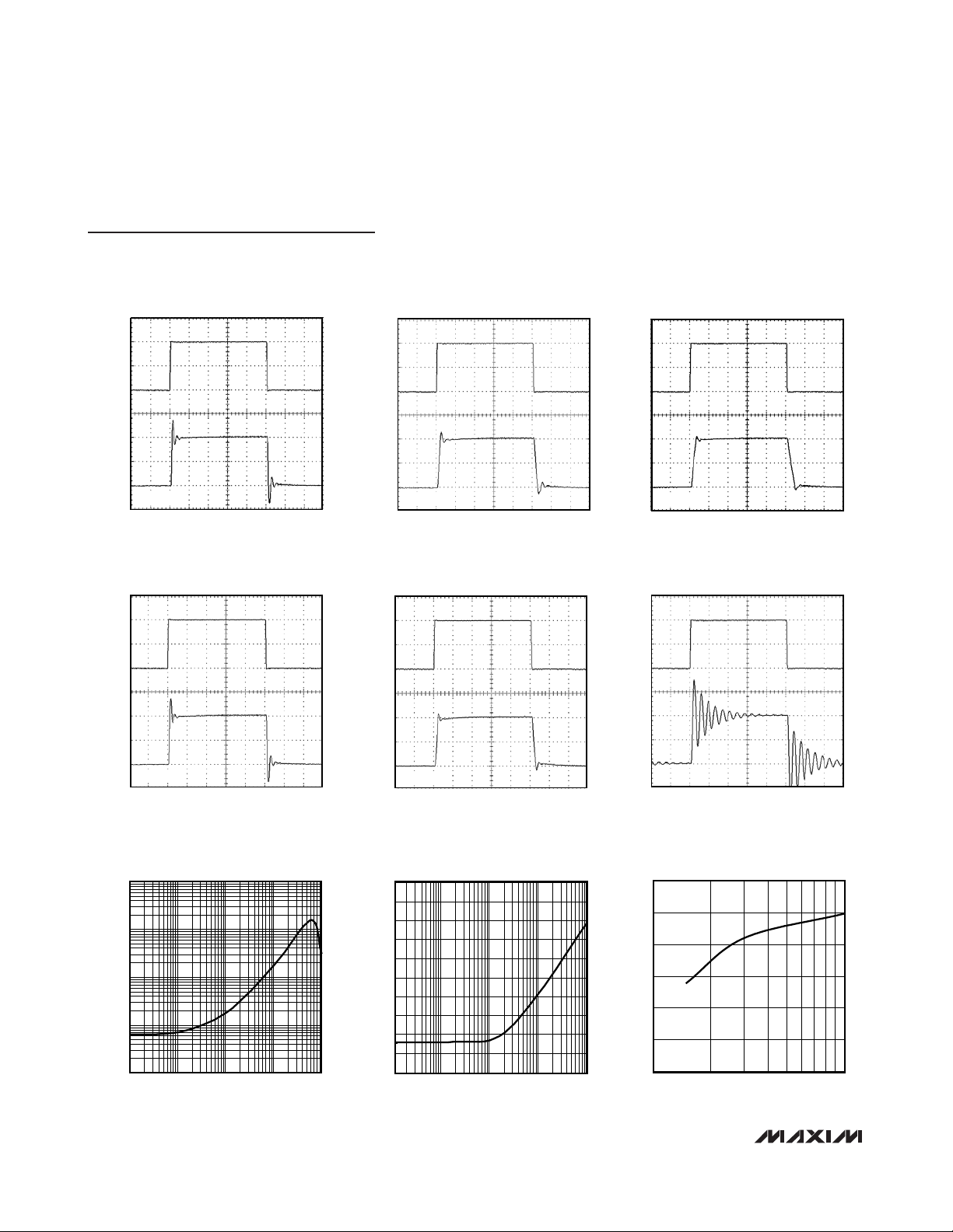
SMALL SIGNAL BANDWIDTH
vs. LOAD RESISTANCE
SMALL-SIGNAL PULSE RESPONSE
INPUT
50mV/div
OUTPUT
50mV/div
RL = 1kΩ
50ns/div
MAX4412 toc11
500mV/div
500mV/div
INPUT
OUTPUT
SMALL-SIGNAL PULSE RESPONSE
INPUT
50mV/div
OUTPUT
50mV/div
MAX4412 toc14
500mV/div
500mV/div
INPUT
OUTPUT
LARGE-SIGNAL PULSE RESPONSE
RL = 1kΩ
50ns/div
LARGE-SIGNAL PULSE RESPONSE
MAX4412 toc12
OUTPUT
MAX4412 toc15
0mV/div
OUTPUT
0mV/div
LARGE-SIGNAL PULSE RESPONSE
INPUT
1V/div
1V/div
RL = 1kΩ
SMALL-SIGNAL PULSE RESPONSE
(C
INPUT
50ns/div
= 15pF)
L
MAX4412 toc13
MAX4412 toc16
RL = 150Ω
MAX4412/MAX4413
CLOSED-LOOP OUTPUT IMPEDANCE
vs. FREQUENCY
1000
100
10
OUTPUT IMPEDANCE (Ω)
1
0.1
100k 1M 100M 1G
50ns/div
10M
FREQUENCY (Hz)
MAX4412 toc17
RL = 150Ω
50ns/div
50ns/div
Low-Cost, Low-Power, Ultra-Small, 3V/5V, 500MHz
Single-Supply Op Amps with Rail-to-Rail Outputs
Typical Operating Characteristics (continued)
(VCC= +5V, VEE= 0, VCM= 1.75V, A
= +1V/V, RF= 24Ω, RL= 1kΩ to VCC/2, CL= 5pF, TA= +25°C, unless otherwise noted.)
VCL
MAX4412/MAX4413
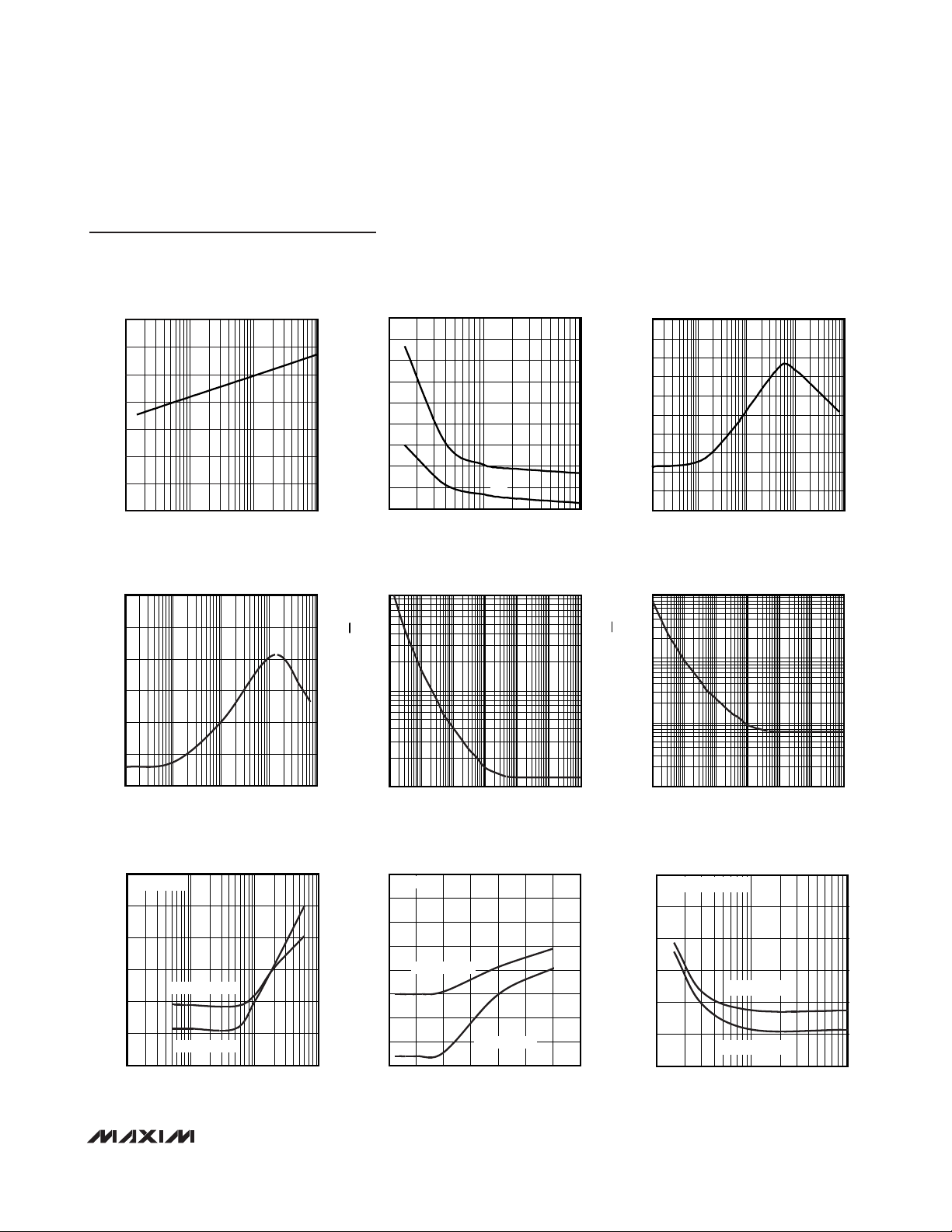
OPEN-LOOP GAIN vs. LOAD RESISTANCE
140
120
100
80
60
OPEN-LOOP GAIN (dB)
40
20
0
100 1k 10k 100k
R
(Ω)
LOAD
COMMON-MODE REJECTION vs.
FREQUENCY
-40
-50
-60
-70
CMR (dB)
-80
450
400
MAX4412 toc20
350
300
250
200
150
100
OUTPUT VOLTAGE SWING (mV)
50
0
100 1k 10k
1000
MAX4412 toc23
100
OUTPUT VOLTAGE SWING vs.
LOAD RESISTANCE
V
OH
V
OL
R
(Ω)
LOAD
VOLTAGE NOISE DENSITY vs.
FREQUENCY
MAX4412 toc21
MAX4412 toc24
POWER SUPPLY REJECTION
vs. FREQUENCY
0
-10
-20
-30
-40
-50
PSR (dB)
-60
-70
-80
-90
-100
100k 1M 10M 100M 1G
FREQUENCY (Hz)
CURRENT NOISE DENSITY vs.
FREQUENCY
100
10
1
MAX4412 toc22
MAX4412 toc25
-90
-100
100k 10M 100M1M 1G
FREQUENCY (Hz)
HARMONIC DISTORTION vs. FREQUENCY
0
V
= 1V
OUT
p-p
-20
-40
-60
DISTORTION (dBc)
-80
-100
-120
100K 1M 10M 100M
2nd HARMONIC
3rd HARMONIC
FREQUENCY (Hz)
________________________________________________________________________________________
MAX4412 toc26
VOLTAGE NOISE DENSITY nV/√Hz
10
1 1k 10k 100k10 100 1M
FREQUENCY (Hz)
HARMONIC DISTORTION vs.
OUTPUT VOLTAGE
-60
f = 5MHz
-65
-70
-75
0 1.0 1.50.5
2nd HARMONIC
3rd HARMONIC
2.0
OUTPUT VOLTAGE (V
-80
-85
DISTORTION (dBc)
-90
-95
-100
2.5 3.0
)
p-p
MAX4412 toc27
3.5
CURRENT NOISE DENSITY pA/√Hz
0
1 1k 10k 100k10 100 1M
FREQUENCY (Hz)
HARMONIC DISTORTION vs.
LOAD RESISTANCE
0
V
= 1V
, f = 5MHz
OUT
p-p
-20
-40
-60
DISTORTION (dBc)
-80
-100
-120
100 1K 10K
2nd HARMONIC
3rd HARMONIC
R
(Ω)
LOAD
MAX4412 toc28
7
MAX4412/MAX4413
Low-Cost, Low-Power, Ultra-Small, 3V/5V, 500MHz
Single-Supply Op Amps with Rail-to-Rail Outputs
8 _______________________________________________________________________________________
Typical Operating Characteristics (continued)
(VCC= +5V, VEE= 0, VCM= 1.75V, A
VCL
= +1V/V, RF= 24Ω, RL= 1kΩ to VCC/2, CL= 5pF, TA= +25°C, unless otherwise noted.)
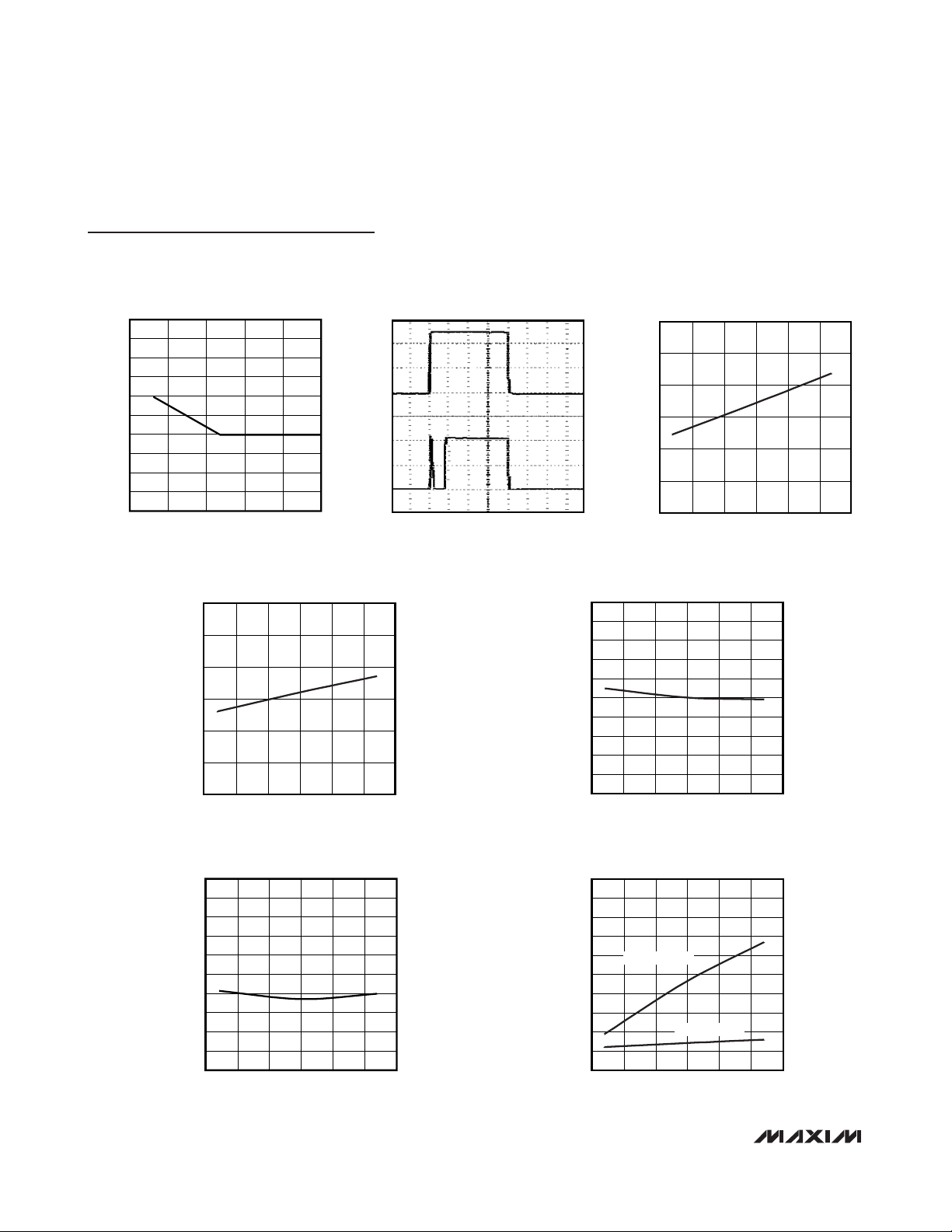
ISOLATION RESISTANCE vs.
CAPACITIVE LOAD
30
28
26
24
22
(Ω)
20
ISO
R
18
16
14
12
10
0 400200 600 800 1000
C
(pF)
LOAD
MAX4412 toc29
750mV/div
V
SUPPLY
2.0V/div
INPUT BIAS CURRENT vs.
TEMPERATURE
3.0
2.5
2.0
1.5
1.0
INPUT BIAS CURRENT (μA)
0.5
0
-50 0 25-25 50 75 100
TEMPERATURE (°C)
INPUT OFFSET VOLTAGE vs.
TEMPERATURE
1.0
0.9
0.8
0.7
0.6
0.5
0.4
0.3
INPUT OFFSET VOLTAGE (mV)
0.2
0.1
0
-50 0-25 25 50 75 100
TEMPERATURE (°C)
POWER-UP RESPONSE TIME
3.0
+5V
2.5
MAX4412 toc30
2.0
0
1.5
+1.5V
V
OUT
500ns/div
1.0
SUPPLY CURRENT (mA)
0.5
0
0
-50 0 25-25 50 75 100
TEMPERATURE
MAX4412 toc31
TEMPERATURE (°C)
INPUT OFFSET CURRENT vs.
TEMPERATURE
SUPPLY CURRENT (PER AMPLIFIER) vs.
100
90
MAX4412 toc32
80
70
60
50
40
30
INPUT OFFSET CURRENT (nA)
20
10
0
-50 0-25 25 50 75 100
TEMPERATURE (°C)
MAX4412 toc33
OUTPUT VOLTAGE SWING vs.
TEMPERATURE
250
225
MAX4412 toc34
200
175
150
125
100
75
OUTPUT VOLTAGE SWING (mV)
50
25
0
VOH = VCC - V
-50 0-25 25 50 75 100
OUT
VOL = V
OUT
TEMPERATURE (°C)
- V
EE
MAX4412 toc35
MAX4412/MAX4413
Low-Cost, Low-Power, Ultra-Small, 3V/5V, 500MHz
Single-Supply Op Amps with Rail-to-Rail Outputs
_______________________________________________________________________________________ 9
Detailed Description
The MAX4412/MAX4413 single-supply, rail-to-rail, voltage-feedback amplifiers achieve 140V/µs slew rates
and 500MHz -3dB bandwidths, while consuming only
1.7mA of supply current per amplifier. Excellent harmonic distortion and differential gain/phase performance make these amplifiers an ideal choice for a wide
variety of video and RF signal-processing applications.
Internal feedback around the output stage ensures low
open-loop output impedance, reducing gain sensitivity
to load variations. This feedback also produces
demand-driven current bias to the output transistors.
Rail-to-Rail Outputs,
Ground-Sensing Input
The MAX4412/MAX4413 input common-mode range
extends from (VEE- 0.1V) to (VCC- 1.5V) with excellent
common-mode rejection. Beyond this range, the amplifier output is a nonlinear function of the input, but does
not undergo phase reversal or latchup.
The output swings to within 105mV of either power-supply rail with a 1kΩ load. Input ground sensing and railto-rail outputs substantially increase the dynamic
range. With a symmetric input in a single +5V application, the input can swing 3.6Vp-p, and the output can
swing 4.6Vp-p with minimal distortion.
Output Capacitive Loading
and Stability
The MAX4412/MAX4413 are optimized for AC performance. They are not designed to drive highly reactive
loads. Such loads decrease phase margin and may
produce excessive ringing and oscillation. The use of
an isolation resistor eliminates this problem (Figure 1).
Figure 2 is a graph of the Optimal Isolation Resistor
(R
ISO
) vs. Capacitive Load.
The Small Signal Gain vs. Frequency with Capacitive
Load and No Isolation Resistor graph in the
Typical
Operating Characteristics
shows how a capacitive load
causes excessive peaking of the amplifier’s frequency
response if the capacitor is not isolated from the amplifier by a resistor. A small isolation resistor (usually 20Ω
to 30Ω) placed before the reactive load prevents ringing and oscillation. At higher capacitive loads, AC performance is controlled by the interaction of the load
capacitance and the isolation resistor. The Small-Signal
Gain vs. Frequency with Capacitive Load and 22Ω
Isolation Resistor graph shows the effect of a 22Ω isolation resistor on closed-loop response.
Coaxial cable and other transmission lines are easily
driven when properly terminated at both ends with their
characteristic impedance. Driving back-terminated
transmission lines essentially eliminates the line’s
capacitance.
___________Applications Information
Choosing Resistor Values
Unity-Gain Configuration
The MAX4412/MAX4413 are internally compensated for
unity gain. When configured for unity gain, the devices
require a 24Ω feedback resistor (R
F
). This resistor
improves AC response by reducing the Q of the parallel LC circuit formed by the parasitic feedback capacitance and inductance.
Pin Description
PIN
MAX4412 MAX4413
1 ⎯ OUT Amplifier Output
⎯ 1 OUTA Amplifier A Output
⎯ 7 OUTB Amplifier B Output
24VEENegative Power Supply
3 ⎯ IN+ Amplifier Noninverting Input
⎯ 3 INA+ Amplifier A Noninverting Input
⎯ 5 INB+ Amplifier B Noninverting Input
4 ⎯ IN- Amplifier Inverting Input
⎯ 2 INA- Amplifier A Inverting Input
⎯ 6 INB- Amplifier B Inverting Input
58VCCPositive Power Supply
NAME FUNCTION

MAX4412/MAX4413
Low-Cost, Low-Power, Ultra-Small, 3V/5V, 500MHz
Single-Supply Op Amps with Rail-to-Rail Outputs
10 ______________________________________________________________________________________
Inverting and Noninverting Configurations
Select the gain-setting feedback (RF) and input (RG)
resistor values that best fit the application. Large resistor values increase voltage noise and interact with the
amplifier’s input and PC board capacitance. This can
generate undesirable poles and zeros and decrease
bandwidth or cause oscillations. For example, a noninverting gain-of-two configuration (RF= RG) using 1kΩ
resistors, combined with 1.8pF of amplifier input capacitance and 1pF of PC board capacitance, causes a
pole at 114MHz. Since this pole is within the amplifier
bandwidth, it jeopardizes stability. Reducing the 1kΩ
resistors to 100Ω extends the pole frequency to
1.14GHz, but could limit output swing by adding 200Ω
in parallel with the amplifier’s load resistor.
Note: For high-gain applications where output offset
voltage is a consideration, choose RS to be equal to the
parallel combination of R
F
and RG(Figures 3a and 3b):
Video Line Driver
The MAX4412/MAX4413 are designed to minimize differential gain error and differential phase error to 0.01%/
0.03° respectively, making them ideal for driving video
loads.
Active Filters
The low distortion and high bandwidth of the
MAX4412/MAX4413 make them ideal for use in active
filter circuits. Figure 4 is a 15MHz lowpass, multiplefeedback active filter using the MAX4412.
Figure 3a. Noninverting Gain Configuration
Figure 3b. Inverting Gain Configuration
Figure 1. Driving a Capacitive Load Through an Isolation
Resistor
Figure 2. Isolation Resistance vs. Capacitive Load
R
G
V
IN
R
BIN
R
F
R
ISO
RFR
×
R
S
=
RFR
G
+
G
R
=
R
R
F
V
= [1+ (RF / RG)] V
OUT
2
1
V
OUT
R
0
IN
GAIN
R
V
OUT
C
L
G
R
S
IN
ISOLATION RESISTANCE vs.
30
28
26
24
22
(Ω)
20
ISO
R
18
16
14
12
10
0 400200 600 800 1000
CAPACITIVE LOAD
C
(pF)
LOAD
MAX4412 toc29
R
IN
G
R
S
R
F
V
OUT
= (RF / RG) V
V
OUT
R
O
IN

MAX4412/MAX4413
Low-Cost, Low-Power, Ultra-Small, 3V/5V, 500MHz
Single-Supply Op Amps with Rail-to-Rail Outputs
______________________________________________________________________________________ 11
ADC Input Buffer
Input buffer amplifiers can be a source of significant
errors in high-speed analog-to-digital converter (ADC)
applications. The input buffer is usually required to
rapidly charge and discharge the ADC’s input, which is
often capacitive (see
Output Capacitive Loading and
Stability
). In addition, since a high-speed ADC’s input
impedance often changes very rapidly during the conversion cycle, measurement accuracy must be maintained using an amplifier with very low output
impedance at high frequencies. The combination of
high speed, fast slew rate, low noise, and a low and
stable distortion overload makes the MAX4412/
MAX4413 ideally suited for use as buffer amplifiers in
high-speed ADC applications.
Layout and Power-Supply Bypassing
These amplifiers operate from a single +2.7V to +5.5V
power supply. Bypass V
CC
to ground with a 0.1µF
capacitor as close to the pin as possible.
Maxim recommends using microstrip and stripline techniques to obtain full bandwidth. Design the PC board
for a frequency greater than 1GHz to prevent amplifier
performance degradation due to board parasitics.
Avoid large parasitic capacitances at inputs and outputs. Whether or not a constant-impedance board is
used, observe the following guidelines:
• Do not use wire-wrap boards due to their high inductance.
• Do not use IC sockets because of the increased parasitic capacitance and inductance.
• Use surface-mount instead of through-hole components for better high-frequency performance.
• Use a PC board with at least two layers; it should be
as free from voids as possible.
• Keep signal lines as short and as straight as possible.
Do not make 90° turns; round all corners.
1
f
=×
0
2
Q
=
RRCC
2312
CC R R
×××
1223
1
++
RR R
1
×××π
C
2
1
2
1
1
3

MAX4412/MAX4413
Low-Cost, Low-Power, Ultra-Small, 3V/5V, 500MHz
Single-Supply Op Amps with Rail-to-Rail Outputs
12 ______________________________________________________________________________________
_
Chip Information
MAX4412 TRANSISTOR COUNT: 99
MAX4413 TRANSISTOR COUNT: 192
PROCESS: Bipolar
Figure 4. Multiple-Feedback Lowpass Filter
+5.0V
R2
150Ω
R1
V
IN
150Ω
C1
100pF
R3
511Ω
C2
15pF
10k
10k
MAX4412
V
OUT

MAX4412/MAX4413
Low-Cost, Low-Power, Ultra-Small, 3V/5V, 500MHz
Single-Supply Op Amps with Rail-to-Rail Outputs
______________________________________________________________________________________ 13
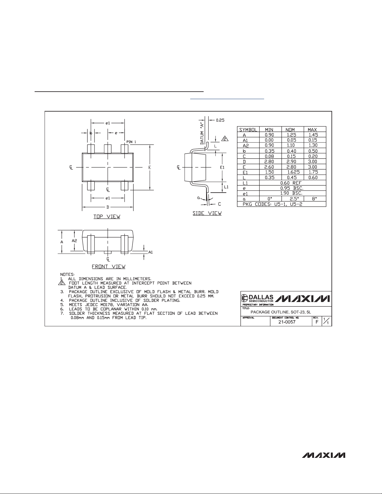
PACKAGE TYPE PACKAGE CODE DOCUMENT NO.
5 SC70 X5-1
21-0076
5 SOT23 U5-2
21-0057
8 SOT23 K8-5
21-0078
Package Information
For the latest package outline information and land patterns, go to www.maxim-ic.com/packages.
SC70, 5L.EPS
PACKAGE OUTLINE, 5L SC70
21-0076
1
E
1
MAX4412/MAX4413
Low-Cost, Low-Power, Ultra-Small, 3V/5V, 500MHz
Single-Supply Op Amps with Rail-to-Rail Outputs
14 ______________________________________________________________________________________
Package Information (continued)
For the latest package outline information and land patterns, go to www.maxim-ic.com/packages.
SOT-23 5L .EPS
MAX4412/MAX4413
Low-Cost, Low-Power, Ultra-Small, 3V/5V, 500MHz
Single-Supply Op Amps with Rail-to-Rail Outputs
______________________________________________________________________________________ 15
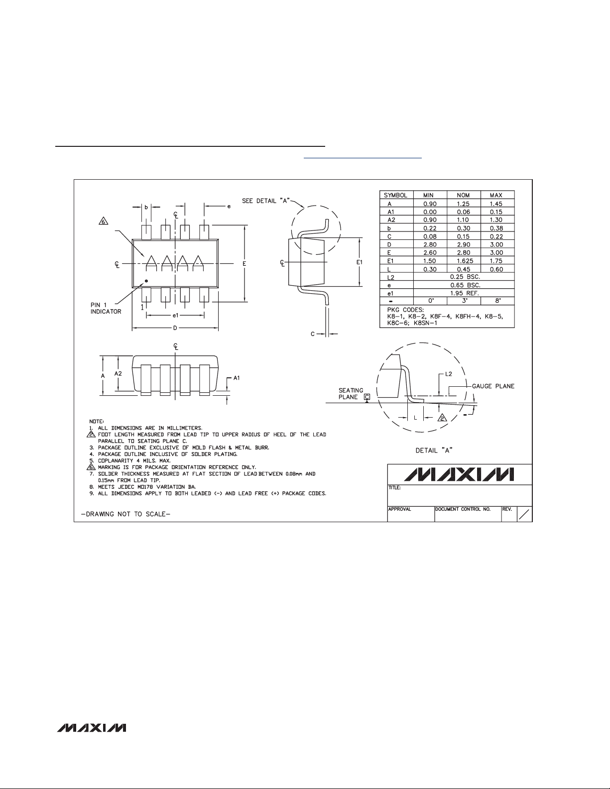
Package Information (continued)
For the latest package outline information and land patterns, go to www.maxim-ic.com/packages.
MARKING
0
SOT23, 8L.EPS
0
PACKAGE OUTLINE, SOT-23, 8L BODY
1
21-0078
1
H

MAX4412/MAX4413
Low-Cost, Low-Power, Ultra-Small, 3V/5V, 500MHz
Single-Supply Op Amps with Rail-to-Rail Outputs
Maxim cannot assume responsibility for use of any circuitry other than circuitry entirely embodied in a Maxim product. No circuit patent licenses are
implied. Maxim reserves the right to change the circuitry and specifications without notice at any time.
16
____________________Maxim Integrated Products, 120 San Gabriel Drive, Sunnyvale, CA 94086 408-737-7600
© 2009 Maxim Integrated Products is a registered trademark of Maxim Integrated Products, Inc.
Revision History
REVISION
NUMBER
0 11/00 Initial release —
1 1/09 Corrected slew rate value 1, 3, 9
REVISION
DATE
DESCRIPTION
PAGES
CHANGED
 Loading...