

General Description
The MAX4409 stereo headphone amplifier combines
Maxim’s DirectDrive™ architecture and a commonmode sense input, which allows the amplifier to reject
common-mode noise. Conventional headphone amplifiers require a bulky DC-blocking capacitor between
the headphone and the amplifier. DirectDrive produces
a ground-referenced output from a single supply, eliminating the need for large DC-blocking capacitors,
which saves cost, board space, and component height.
The common-mode voltage sensing corrects for any
difference between SGND of the amplifier and the
headphone return. This feature minimizes ground-loop
noise when the HP socket is used as a line out connection to other grounded equipment, for example, a PC
connected to a home hi-fi system.
The MAX4409 draws only 5mA of supply current, delivers up to 80mW per channel into a 16Ω load, and has a
low 0.002% THD+N. A high 86dB power-supply rejection ratio allows this device to operate from noisy digital
supplies without additional power-supply conditioning.
The MAX4409 includes ±8kV ESD protection on the
headphone outputs. Comprehensive click-and-pop circuitry eliminates audible clicks and pops on startup
and shutdown. A low-power shutdown mode reduces
supply current draw to only 6µA.
The MAX4409 operates from a single 1.8V to 3.6V supply, has short-circuit and thermal overload protection,
and is specified over the extended -40°C to +85°C temperature range. The MAX4409 is available in tiny 20-pin
thin QFN (4mm x 4mm x 0.8mm) and 14-pin TSSOP
packages.
Applications
Features
♦ No Bulky DC-Blocking Capacitors Required
♦ Ground-Referenced Outputs Eliminate DC-Bias
Voltages on Headphone Ground Pin
♦ Common-Mode Voltage Sensing Eliminates
Ground-Loop Noise
♦ 96dB CMRR
♦ No Degradation of Low-Frequency Response Due
to Output Capacitors
♦ 80mW per Channel into 16Ω
♦ Low 0.002% THD+N
♦ High 86dB PSRR
♦ Integrated Click-and-Pop Suppression
♦ 1.8V to 3.6V Single-Supply Operation
♦ Low Quiescent Current
♦ Low-Power Shutdown Mode
♦ Short-Circuit and Thermal-Overload Protection
♦ ±8kV ESD-Protected Amplifier Outputs
♦ Available in Space-Saving Packages
14-Pin TSSOP
20-Pin Thin QFN (4mm x 4mm x 0.8mm)
MAX4409
80mW, DirectDrive, Stereo Headphone
Amplifier with Common-Mode Sense
________________________________________________________________ Maxim Integrated Products 1
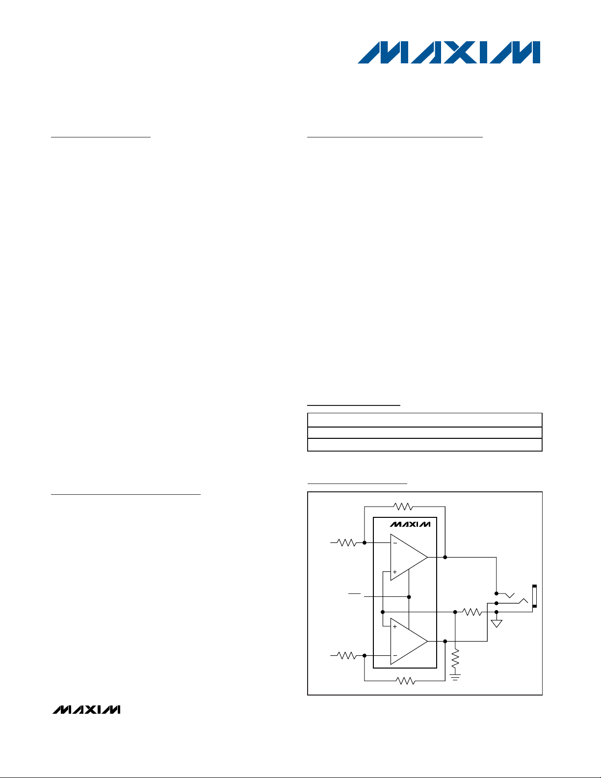
LEFT
AUDIO
INPUT
RIGHT
AUDIO
INPUT
SHDN
COM
MAX4409
DirectDrive OUTPUTS
ELIMINATE DC-BLOCKING
CAPACITORS
COMMON-MODE
SENSE INPUT ELIMINATES
GROUND-LOOP NOISE
Functional Diagram
Ordering Information
19-2842; Rev 2; 11/07
For pricing, delivery, and ordering information, please contact Maxim Direct at 1-888-629-4642,
or visit Maxim’s website at www.maxim-ic.com
PART
PIN-PACKAGE
MAX4409ETP
20 Thin QFN-EP*
MAX4409EUD
14 TSSOP
Notebooks
Desktop PCs
Cellular Phones
PDAs
MP3 Players
Tablet PCs
Portable Audio Equipment
Pin Configurations and Typical Application Circuit appear
at end of data sheet.
*EP = Exposed paddle.
TEMP RANGE
-40°C to +85°C
-40°C to +85°C
MAX4409
80mW, DirectDrive, Stereo Headphone
Amplifier with Common-Mode Sense
2 _______________________________________________________________________________________
ABSOLUTE MAXIMUM RATINGS
ELECTRICAL CHARACTERISTICS
(PVDD= SVDD= 3V, PGND = SGND = 0V, SHDN = SVDD, C1 = C2 = 2.2µF, RIN= RF= R1 = R2 = 10kΩ, RL= ∞, TA= T
MIN
to T
MAX
,
unless otherwise noted. Typical values are at T
A
= +25°C.) (Note 2)
Stresses beyond those listed under “Absolute Maximum Ratings” may cause permanent damage to the device. These are stress ratings only, and functional
operation of the device at these or any other conditions beyond those indicated in the operational sections of the specifications is not implied. Exposure to
absolute maximum rating conditions for extended periods may affect device reliability.
PGND to SGND .....................................................-0.3V to +0.3V
PV
DD
to SV
DD .................................................................
-0.3V to +0.3V
PV
SS
to SVSS.........................................................-0.3V to +0.3V
PV
DD
and SVDDto PGND or SGND .........................-0.3V to +4V
PV
SS
and SVSSto PGND or SGND ..........................-4V to +0.3V
IN_ and COM to SGND.................................SV
SS
to (SVDD- 1V)
IN_ to COM .....................................(COM + 2V) to (COM - 0.3V)
SHDN_ to SGND........................(SGND - 0.3V) to (SV
DD
+ 0.3V)
OUT_ to SGND ............................(SV
SS
- 0.3V) to (SVDD+ 0.3V)
C1P to PGND.............................(PGND - 0.3V) to (PV
DD
+ 0.3V)
C1N to PGND .............................(PV
SS
- 0.3V) to (PGND + 0.3V)
Output Short Circuit to GND or V
DD
...........................Continuous
Thermal Limits (Note 1)
Continuous Power Dissipation (T
A
= +70°C)
20-Pin Thin QFN Multilayer (derate 25.6mW/°C
above +70°C).............................................................2051mW
θ
JA
................................................................................39°C/W
θ
JC
...............................................................................5.7°C/W
14-Pin TSSOP Multilayer (derate 10mW/°C
above +70°C)...............................................................797mW
θ
JA
..............................................................................100°C/W
θ
JC
................................................................................30°C/W
Junction Temperature......................................................+150°C
Operating Temperature Range ...........................-40°C to +85°C
Storage Temperature Range .............................-65°C to +150°C
Lead Temperature (soldering, 10s) .................................+300°C
PARAMETER
CONDITIONS
UNITS
Supply Voltage Range V
DD
Guaranteed by PSRR test
3.6 V
Quiescent Supply Current I
DD
5 8.4 mA
Shutdown Supply Current I
SHDN
SHDN = GND 6 10 µA
V
IH
0.7 x
SHDN Thresholds
V
IL
0.3 x
V
SHDN Input Leakage Current -1 +1 µA
SHDN to Full Operation t
SON
µs
CHARGE PUMP
Oscillator Frequency f
OSC
kHz
AMPLIFIERS
Input Offset Voltage V
OS
RL = 32Ω
2.4 mV
Input Bias Current I
BIAS
0nA
COM Bias Current I
COM
0nA
Equivalent Input Offset Current I
OS
IOS = (I
BIAS(INR)
+ I
BIAS(INL)
- I
COM
) / 2 ±2 nA
COM Input Range V
COM
Inferred from CMRR test
mV
Common-Mode Rejection Ratio CMRR -500mV ≤ V
COM
≤ +500mV, R
SOURCE
≤ 10Ω 75 96 dB
1.8V ≤ VDD ≤ 3.6V DC (Note 3) 75 86
76Power-Supply Rejection Ratio PSRR
V
DD
= 3.0V,
200mV
P-P
ripple (Note 4)
48
dB
RL = 32Ω 65
Output Power P
OUT
RL = 16Ω 55 80
mW
Note 1: Package thermal resistances were obtained using the method described in JEDEC specification JESD51-7, using a 4-layer
board. For detailed information on package thermal considerations see www.maxim-ic.com/thermal-tutorial
.
SYMBOL
MIN TYP MAX
1.8
SV
DD
175
272 320 368
0.5
-700 -100
-1400 -200
-500 +500
THD+N = 1%, TA = +25°C
f
RIPPLE
f
RIPPLE
= 1kHz
= 20kHz
SV
DD
MAX4409
80mW, DirectDrive, Stereo Headphone
Amplifier with Common-Mode Sense
_______________________________________________________________________________________ 3
ELECTRICAL CHARACTERISTICS (continued)
(PVDD= SVDD= 3V, PGND = SGND = 0V, SHDN = SVDD, C1 = C2 = 2.2µF, RIN= RF= R1 = R2 = 10kΩ, RL= ∞, TA= T
MIN
to T
MAX
,
unless otherwise noted. Typical values are at T
A
= +25°C.) (Note 2)
Note 2: All specifications are 100% tested at TA= +25°C; temperature limits are guaranteed by design.
Note 3: Inputs are connected to ground and COM.
Note 4: Inputs are AC-coupled to ground. COM is connected to ground.
PARAMETER
SYMBOL
CONDITIONS
MIN
TYP
MAX
UNITS
RL = 32Ω,
P
OUT
= 50mW
Total Harmonic Distortion
Plus Noise
fIN = 1kHz
R
L
= 16Ω,
P
OUT
= 60mW
%
Signal-to-Noise Ratio (Note 4) SNR RL = 32Ω, P
OUT
= 20mW, fIN = 1kHz 95 dB
Slew Rate SR
V/µs
Maximum Capacitive Load C
L
No sustained oscillations
pF
Crosstalk RL = 16Ω, P
OUT
= 1.6mW, fIN = 10kHz 55 dB
Thermal Shutdown Threshold
°C
Thermal Shutdown Hysteresis 15 °C
ESD Protection Human Body Model (OUTR, OUTL) ±8 kV
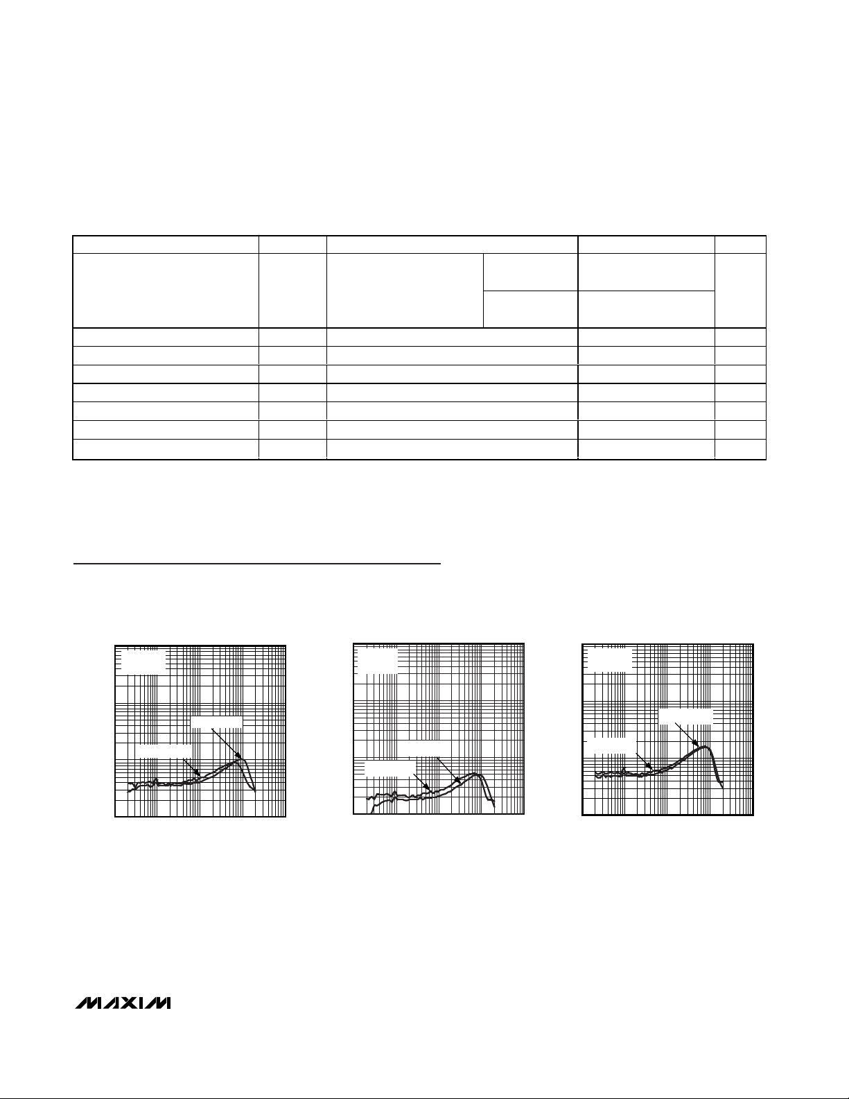
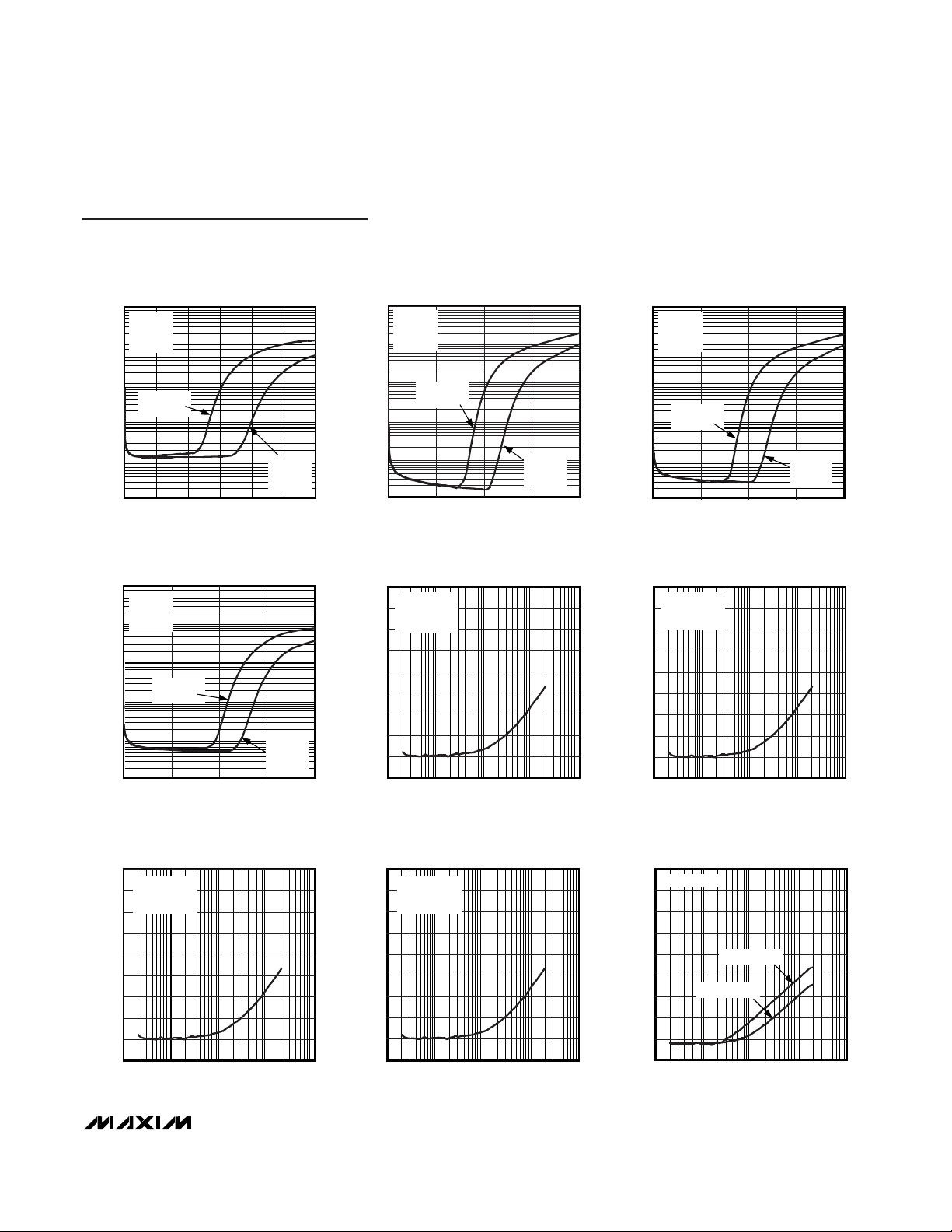
Typical Operating Characteristics
(C1 = C2 = 2.2µF, R
IN
= RF= R1 = R2 = 10kΩ, THD+N measurement bandwidth = 22Hz to 22kHz, TA= +25°C, unless otherwise noted.)
10 100 10k1k 100k
TOTAL HARMONIC DISTORTION PLUS
NOISE vs. FREQUENCY
MAX4409 toc01
FREQUENCY (Hz)
THD+N (%)
1
0.1
0.001
0.01
VDD = 3V
R
L
= 16
Ω
P
OUT
= 10mW
P
OUT
= 60mW
1
0.001
TOTAL HARMONIC DISTORTION PLUS
NOISE vs. FREQUENCY
0.01
0.1
MAX4409 toc02
THD+N (%)
10 100 10k1k 100k
FREQUENCY (Hz)
VDD = 3V
R
L
= 32Ω
P
OUT
= 50mW
P
OUT
= 10mW
TOTAL HARMONIC DISTORTION PLUS
NOISE vs. FREQUENCY
MAX4409 toc03
THD+N (%)
1
0.1
0.001
0.01
VDD = 1.8V
R
L
= 16Ω
P
OUT
= 5mW
P
OUT
= 15mW
10 100 10k1k 100k
FREQUENCY (Hz)
0.002
THD+N
0.005
0.8
150
140
MAX4409
80mW, DirectDrive, Stereo Headphone
Amplifier with Common-Mode Sense
4 _______________________________________________________________________________________
Typical Operating Characteristics (continued)
(C1 = C2 = 2.2µF, R
IN
= RF= R1 = R2 = 10kΩ, THD+N measurement bandwidth = 22Hz to 22kHz, TA= +25°C, unless otherwise noted.)
1
TOTAL HARMONIC DISTORTION PLUS
NOISE vs. FREQUENCY
0.001
0.01
0.1
MAX4409 toc04
VDD = 1.8V
R
L
= 32Ω
THD+N (%)
P
OUT
= 15mW
P
OUT
= 5mW
10 100 10k1k 100k
FREQUENCY (Hz)
100
10
1
0.1
0.01
0.001
090
120
150
30 60
180
TOTAL HARMONIC DISTORTION PLUS
NOISE vs. OUTPUT POWER
MAX4409 toc05
OUTPUT POWER (W)
THD+N (%)
VDD = 3V
f = 20Hz
R
L
= 16Ω
OUTPUTS
OUT OF
PHASE
OUTPUTS
IN PHASE
100
10
1
0.1
0.01
0.001
090
120
150
30 60
180
TOTAL HARMONIC DISTORTION PLUS
NOISE vs. OUTPUT POWER
MAX4409 toc06
OUTPUT POWER (W)
THD+N (%)
VDD = 3V
f = 1kHz
R
L
= 16Ω
OUTPUTS IN
PHASE
OUTPUTS
OUT OF
PHASE
100
10
1
0.1
0.01
0.001
09060
120 150
30 180
TOTAL HARMONIC DISTORTION PLUS
NOISE vs. OUTPUT POWER
MAX4409 toc07
OUTPUT POWER (W)
THD+N (%)
VDD = 3V
f = 10kHz
R
L
= 16Ω
OUTPUTS IN
PHASE
OUTPUTS
OUT OF
PHASE
100
10
1
0.1
0.01
0.001
0.0001
0
40
60
8020
120
100
TOTAL HARMONIC DISTORTION PLUS
NOISE vs. OUTPUT POWER
MAX4409 toc08
OUTPUT POWER (W)
THD+N (%)
VDD = 3V
f = 20Hz
R
L
= 32Ω
OUTPUTS IN
PHASE
OUTPUTS
OUT OF
PHASE
100
10
1
0.1
0.01
0.001
0
40 100
60
80
20 120
TOTAL HARMONIC DISTORTION PLUS
NOISE vs. OUTPUT POWER
MAX4409 toc09
OUTPUT POWER (W)
THD+N (%)
VDD = 3V
f = 1kHz
R
L
= 32Ω
OUTPUTS IN
PHASE
OUTPUTS
OUT OF
PHASE
100
10
1
0.1
0.01
0.001
0 40 100
8060
20 120
TOTAL HARMONIC DISTORTION PLUS
NOISE vs. OUTPUT POWER
MAX4409 toc10
OUTPUT POWER (W)
THD+N (%)
VDD = 3V
f = 10kHz
R
L
= 32Ω
OUTPUTS IN
PHASE
OUTPUTS
OUT OF
PHASE
100
10
1
0.1
0.01
0.001
02040503010 60
TOTAL HARMONIC DISTORTION PLUS
NOISE vs. OUTPUT POWER
MAX4409 toc11
OUTPUT POWER (W)
THD+N (%)
VDD = 1.8V
f = 20Hz
R
L
= 16Ω
OUTPUTS IN
PHASE
OUTPUTS
OUT OF
PHASE
100
10
1
0.1
0.01
0.001
02040503010 60
TOTAL HARMONIC DISTORTION PLUS
NOISE vs. OUTPUT POWER
MAX4409 toc12
OUTPUT POWER (W)
VDD = 1.8V
f = 1kHz
R
L
= 16Ω
THD+N (%)
OUTPUTS IN
PHASE
OUTPUTS
OUT OF
PHASE
MAX4409
80mW, DirectDrive, Stereo Headphone
Amplifier with Common-Mode Sense
_______________________________________________________________________________________ 5
100
10
1
0.1
0.01
0.001
02040503010 60
TOTAL HARMONIC DISTORTION PLUS
NOISE vs. OUTPUT POWER
MAX4409 toc13
OUTPUT POWER (W)
VDD = 1.8V
f = 10kHz
R
L
= 16Ω
THD+N (%)
OUTPUTS IN
PHASE
OUTPUTS
OUT OF
PHASE
100
10
1
0.1
0.01
0.001
03040
2010
TOTAL HARMONIC DISTORTION PLUS
NOISE vs. OUTPUT POWER
MAX4409 toc14
OUTPUT POWER (W)
THD+N (%)
VDD = 1.8V
f = 20Hz
R
L
= 32Ω
OUTPUTS IN
PHASE
OUTPUTS
OUT OF
PHASE
100
10
1
0.1
0.01
0.001
020403010
TOTAL HARMONIC DISTORTION PLUS
NOISE vs. OUTPUT POWER
MAX4409 toc15
OUTPUT POWER (W)
THD+N (%)
VDD = 1.8V
f = 1kHz
R
L
= 32Ω
OUTPUTS IN
PHASE
OUTPUTS
OUT OF
PHASE
100
10
1
0.1
0.01
0.001
0
20 30
40
10
TOTAL HARMONIC DISTORTION PLUS
NOISE vs. OUTPUT POWER
MAX4409 toc16
OUTPUT POWER (W)
THD+N (%)
VDD = 1.8V
f = 10kHz
R
L
= 32Ω
OUTPUTS IN
PHASE
OUTPUTS
OUT OF
PHASE
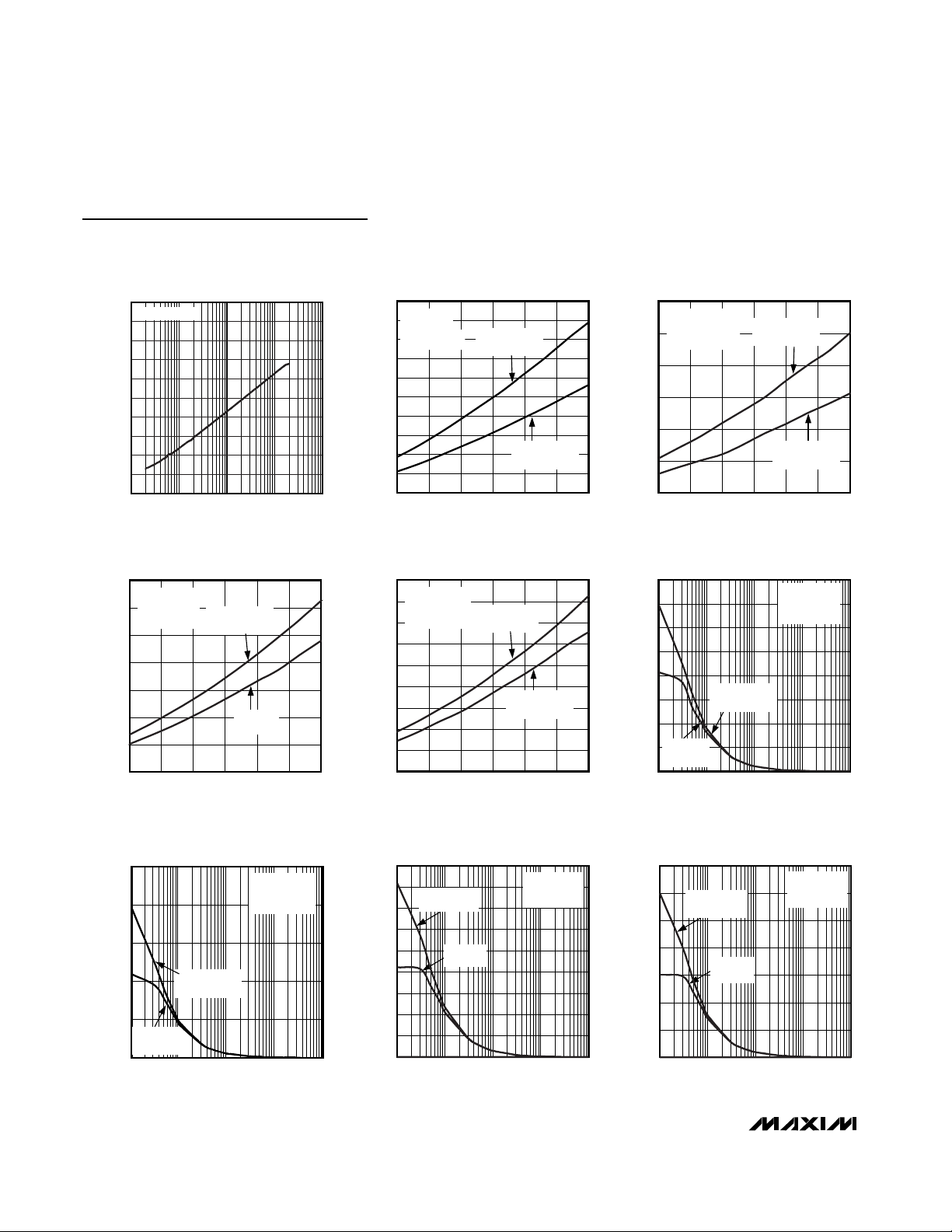
10 100 10k1k 100k
POWER-SUPPLY REJECTION RATIO
vs. FREQUENCY
MAX4409 toc17
FREQUENCY (Hz)
PSRR (dB)
0
-30
-40
-20
-10
-90
-70
-80
-50
-60
VDD = 3V
V
IN
= 200mV
P-P
RL = 16Ω
10 100 10k1k 100k
POWER-SUPPLY REJECTION RATIO
vs. FREQUENCY
MAX4410 toc18
FREQUENCY (Hz)
PSRR (dB)
0
-40
-10
-20
-30
-90
-70
-80
-50
-60
VDD = 3V
V
IN
= 200mV
P-P
RL = 16Ω
10 100 10k1k 100k
POWER-SUPPLY REJECTION RATIO
vs. FREQUENCY
MAX4410 toc19
FREQUENCY (Hz)
PSRR (dB)
0
-40
-10
-20
-30
-90
-70
-80
-50
-60
VDD = 1.8V
V
IN
= 200mV
P-P
RL = 16Ω
10 100 10k1k 100k
POWER-SUPPLY REJECTION RATIO
vs. FREQUENCY
MAX4410 toc20
FREQUENCY (Hz)
PSRR (dB)
0
-40
-10
-20
-30
-90
-70
-80
-60
-50
VDD = 1.8V
V
IN
= 200mV
P-P
RL = 32Ω
CROSSTALK vs. FREQUENCY
MAX4410 toc21
FREQUENCY (Hz)
CROSSTALK (dB)
10k1k100
-80
-60
-70
-40
-50
-10
-20
-30
0
-90
10 100k
LEFT TO RIGHT
RIGHT TO LEFT
VIN = 200mV
P-P
Typical Operating Characteristics (continued)
(C1 = C2 = 2.2µF, R
IN
= RF= R1 = R2 = 10kΩ, THD+N measurement bandwidth = 22Hz to 22kHz, TA= +25°C, unless otherwise noted.)
MAX4409
80mW, DirectDrive, Stereo Headphone
Amplifier with Common-Mode Sense
6 _______________________________________________________________________________________
Typical Operating Characteristics (continued)
(C1 = C2 = 2.2µF, R
IN
= RF= R1 = R2 = 10kΩ, THD+N measurement bandwidth = 22Hz to 22kHz, TA= +25°C, unless otherwise noted.)
COMMON-MODE REJECTION RATIO
vs. FREQUENCY
MAX4409 toc22
FREQUENCY (Hz)
CMRR (dB)
10k1k100
-90
-70
-80
-40
-50
-60
-10
-20
-30
0
-100
10 100k
VIN = 500mV
P-P
OUTPUT POWER vs. SUPPLY VOLTAGE
MAX4409 toc23
SUPPLY VOLTAGE (V)
OUTPUT POWER (mW)
3.33.02.72.42.1
20
40
60
80
100
120
140
160
180
200
0
1.8 3.6
fIN = 1kHz
R
L
= 16Ω
THD+N = 1%
INPUTS
IN PHASE
INPUTS 180°
OUT OF PHASE
OUTPUT POWER vs. SUPPLY VOLTAGE
MAX4409 toc24
SUPPLY VOLTAGE (V)
OUTPUT POWER (mW)
3.33.02.72.42.1
50
100
150
200
250
300
0
1.8 3.6
fIN = 1kHz
R
L
= 16Ω
THD+N = 10%
INPUTS
IN PHASE
INPUTS 180°
OUT OF PHASE
OUTPUT POWER vs. SUPPLY VOLTAGE
MAX4409 toc25
SUPPLY VOLTAGE (V)
OUTPUT POWER (mW)
3.33.02.72.42.1
20
40
60
80
100
120
140
0
1.8 3.6
fIN = 1kHz
R
L
= 32Ω
THD+N = 1%
INPUTS 180°
OUT OF PHASE
INPUTS
IN PHASE
OUTPUT POWER vs. SUPPLY VOLTAGE
MAX4409 toc26
SUPPLY VOLTAGE (V)
OUTPUT POWER (mW)
3.33.02.72.42.1
40
20
60
80
100
120
140
160
180
0
1.8 3.6
fIN = 1kHz
R
L
= 32Ω
THD+N = 10%
INPUTS
IN PHASE
INPUTS 180°
OUT OF PHASE
OUTPUT POWER vs. LOAD RESISTANCE
MAX4409 toc27
LOAD RESISTANCE (Ω)
OUTPUT POWER (mW)
10k1k100
40
20
60
80
100
120
140
160
0
10 100k
VDD = 3V
f
IN
= 1kHz
THD+N = 1%
INPUTS 180°
OUT OF PHASE
INPUTS
IN PHASE
OUTPUT POWER vs. LOAD RESISTANCE
MAX4409 toc28
LOAD RESISTANCE (Ω)
OUTPUT POWER (mW)
10k1k100
50
100
150
200
250
0
10 100k
INPUTS
IN PHASE
INPUTS 180°
OUT OF PHASE
VDD = 3V
f
IN
= 1kHz
THD+N = 10%
OUTPUT POWER vs. LOAD RESISTANCE
MAX4409 toc29
LOAD RESISTANCE (Ω)
OUTPUT POWER (mW)
10k1k100
5
10
15
20
25
30
35
40
45
0
10 100k
INPUTS 180°
OUT OF PHASE
INPUTS IN
PHASE
VDD = 1.8V
f
IN
= 1kHz
THD+N = 1%
OUTPUT POWER vs. LOAD RESISTANCE
MAX4409 toc30
LOAD RESISTANCE (Ω)
OUTPUT POWER (mW)
10k1k100
10
20
30
40
50
60
70
0
10 100k
INPUTS 180°
OUT OF PHASE
INPUTS IN
PHASE
VDD = 1.8V
f
IN
= 1kHz
THD+N = 10%

MAX4409
80mW, DirectDrive, Stereo Headphone
Amplifier with Common-Mode Sense
_______________________________________________________________________________________ 7
POWER DISSIPATION
vs. OUTPUT POWER
MAX4409 toc31
OUTPUT POWER (mW)
POWER DISSIPATION (mW)
16012040 80
50
100
150
200
250
300
350
400
0
0 200
INPUTS 180°
OUT OF PHASE
fIN = 1kHz
R
L
= 16Ω
V
DD
= 3V
P
OUT
= P
OUTL + POUTR
INPUTS
IN PHASE
POWER DISSIPATION
vs. OUTPUT POWER
MAX4409 toc32
OUTPUT POWER (mW)
POWER DISSIPATION (mW)
16012040 80
20
40
60
80
120
100
140
160
180
0
0200
INPUTS 180°
OUT OF PHASE
fIN = 1kHz
R
L
= 32Ω
V
DD
= 3V
P
OUT
= P
OUTL + POUTR
INPUTS
IN PHASE
POWER DISSIPATION
vs. OUTPUT POWER
MAX4409 toc33
OUTPUT POWER (mW)
POWER DISSIPATION (mW)
50403010 20
20
40
60
80
100
120
140
0
060
INPUTS 180°
OUT OF PHASE
fIN = 1kHz
R
L
= 16Ω
V
DD
= 1.8V
P
OUT
= P
OUTL + POUTR
INPUTS
IN PHASE
POWER DISSIPATION
vs. OUTPUT POWER
MAX4409 toc34
OUTPUT POWER (mW)
POWER DISSIPATION (mW)
50403010 20
10
20
30
40
50
60
70
0
060
INPUTS 180°
OUT OF PHASE
fIN = 1kHz
R
L
= 32Ω
V
DD
= 1.8V
P
OUT
= P
OUTL + POUTR
INPUTS
IN PHASE
80
60
40
100 10k 100k 1M 10M
20
0
-20
-40
-60
-80
-100
-180
-120
-140
-160
GAIN AND PHASE vs. FREQUENCY
MAX4409 toc35
FREQUENCY (Hz)
GAIN/PHASE (dB/DEGREES)
VDD = 3V
A
V
= 1000V/V
R
L
= 16Ω
1k
GAIN
PHASE
10
10 1k 10k 1M100k 10M
0
-10
-20
-30
-50
-40
GAIN FLATNESS vs. FREQUENCY
MAX4410 toc36
FREQUENCY (Hz)
GAIN (dB)
VDD = 3V
A
V
= -1V/V
R
L
= 16Ω
100
CHARGE-PUMP OUTPUT RESISTANCE
vs. SUPPLY VOLTAGE
MAX4409 toc37
SUPPLY VOLTAGE (V)
OUTPUT RESISTANCE (Ω)
3.33.02.72.42.1
2
4
6
8
10
0
1.8 3.6
V
IN_
= GND
I
PVSS
= 10mA
NO LOAD
OUTPUT POWER vs. CHARGE-PUMP
CAPACITANCE AND LOAD RESISTANCE
MAX4409 toc38
LOAD RESISTANCE (Ω)
OUTPUT POWER (mW)
403020
20
10
30
40
50
60
70
80
90
0
10 50
fIN = 1kHz
THD+N = 1%
INPUTS IN PHASE
C1 = C2 = 1μF
C1 = C2 = 0.47μF
C1 = C2 = 0.68μF
C1 = C2 = 2.2μF
FREQUENCY (Hz)
10k1k
100 100k
OUTPUT SPECTRUM vs. FREQUENCY
MAX4409 toc39
OUTPUT SPECTRUM (dB)
-100
-80
-60
-40
-20
0
-120
VIN = 1V
P-P
fIN = 1kHz
R
L
= 32Ω
A
V
= -1V/V
Typical Operating Characteristics (continued)
(C1 = C2 = 2.2µF, R
IN
= RF= R1 = R2 = 10kΩ, THD+N measurement bandwidth = 22Hz to 22kHz, TA= +25°C, unless otherwise noted.)

MAX4409
80mW, DirectDrive, Stereo Headphone
Amplifier with Common-Mode Sense
8 _______________________________________________________________________________________
Pin Description
PIN
TSSOP
FUNCTION
118
Common-Mode Voltage Sense Input
219
Charge-Pump Power Supply. Powers charge-pump inverter, charge-pump logic, and
oscillator.
3 1 C1P Flying Capacitor Positive Terminal
42
Power Ground. Connect to SGND.
5 3 C1N Flying Capacitor Negative Terminal
65
Charge-Pump Output
77
Amplifier Negative Power Supply. Connect to PVSS.
89
Left-Channel Output
910
Amplifier Positive Power Supply. Connect to PVDD.
10 13 INL Left-Channel Audio Input
11 11
Right-Channel Output
12 14
Active-Low Shutdown. Connect to VDD for normal operation.
13 15 INR Right-Channel Audio Input
14 17
Signal Ground. Connect to PGND.
—
4, 6, 8, 12,
16, 20
N.C. No Connection. Not internally connected.
— — EP Exposed Paddle. Leave unconnected. Do not connect to VDD or GND.
Typical Operating Characteristics (continued)
(C1 = C2 = 2.2µF, R
IN
= RF= R1 = R2 = 10kΩ, THD+N measurement bandwidth = 22Hz to 22kHz, TA= +25°C, unless otherwise noted.)
SUPPLY CURRENT
vs. SUPPLY VOLTAGE
MAX4409 toc40
SUPPLY VOLTAGE (V)
SUPPLY CURRENT (mA)
2.71.80.9
2
4
6
8
10
0
03.6
SHUTDOWN SUPPLY CURRENT
vs. SUPPLY VOLTAGE
MAX4409 toc41
SUPPLY VOLTAGE (V)
SUPPLY CURRENT (μA)
2.71.80.9
2
4
6
8
10
0
03.6
SHDN = GND
POWER-UP/DOWN WAVEFORM
MAX4409 toc42
OUT_
OUT_FFT
V
DD
3V
20dB/div
10mV/div
0V
200ms/div
FFT: 25Hz/div
R
L
= 32Ω
V
IN_
= GND
-100dB
THIN QFN
NAME
COM
PV
DD
PGND
PV
SS
SV
SS
OUTL
SV
DD
OUTR
SHDN
SGND

MAX4409
80mW, DirectDrive, Stereo Headphone
Amplifier with Common-Mode Sense
_______________________________________________________________________________________ 9
Detailed Description
The MAX4409 stereo headphone driver features Maxim’s
patented DirectDrive architecture, eliminating the large
output-coupling capacitors required by traditional singlesupply headphone drivers. The device consists of two
80mW Class AB headphone drivers, undervoltage lockout (UVLO)/shutdown control, charge-pump, and comprehensive click-and-pop suppression circuitry (see
Typical Application Circuit). The charge pump inverts the
positive supply (PV
DD
), creating a negative supply
(PVSS). The headphone drivers operate from these bipolar supplies with their outputs biased about GND (Figure
1). The drivers have almost twice the supply range compared to other 3V single-supply drivers, increasing the
available output power. The benefit of this GND bias is
that the driver outputs do not have a DC component typically V
DD
/2. Thus, the large DC-blocking capacitors are
unnecessary, improving frequency response while conserving board space and system cost.
The MAX4409 also features a common-mode voltage
sense input that corrects for mismatch between the
SGND of the device and the potential at the headphone
jack return. A low-power shutdown mode reduces supply current to 6µA. The device features an undervoltage
lockout that prevents operation from an insufficient
power supply and click-and-pop suppression that eliminates audible transients on startup and shutdown.
Additionally, the MAX4409 features thermal overload
and short-circuit protection and can withstand ±8kV
ESD strikes on the output pins.
Common-Mode Sense
When the headphone jack is used as a line out to interface between other equipment (notebooks, desktops,
and stereo receivers), potential differences between
the equipment grounds can create ground loops and
excessive ground current flow. The MAX4409 COM
input senses and corrects for the difference between
the headphone return and device ground. Connect
COM through a resistive voltage-divider between the
headphone jack return and SGND of the device (see
Typical Application Circuit). For optimum commonmode rejection, use the same value resistors for R2 and
RIN, and R1 and RF. Improve DC CMRR by adding a
capacitor in between with SGND and R2 (see Typical
Application Circuit). If ground sensing is not required,
connect COM directly to SGND through a 5kΩ resistor.
DirectDrive
Traditional single-supply headphone drivers have their
outputs biased about a nominal DC voltage (typically
half the supply) for maximum dynamic range. Large
coupling capacitors are needed to block this DC bias
from the headphone. Without these capacitors, a significant amount of DC current flows to the headphone,
resulting in unnecessary power dissipation and possible damage to both headphone and headphone driver.
Maxim’s patented DirectDrive architecture uses a
charge pump to create an internal negative supply voltage. This allows the outputs of the MAX4409 to be
biased about GND, almost doubling dynamic range
while operating from a single supply. With no DC component, there is no need for the large DC-blocking
capacitors. Instead of two large (220µF, typ) tantalum
capacitors, the MAX4409 charge pump requires two
small ceramic capacitors, thereby conserving board
space, reducing cost, and improving the frequency
response of the headphone driver. See the Output
Power vs. Charge-Pump Capacitance and Load
Resistance graph in the Typical Operating Char-
acteristics for details of the possible capacitor sizes.
There is a low DC voltage on the driver outputs due to
amplifier offset. However, the offset of the MAX4409 is
+V
DD
-V
DD
GND
V
OUT
CONVENTIONAL DRIVER-BIASING SCHEME
DirectDrive BIASING SCHEME
VDD/2
V
DD
GND
V
OUT
Figure 1. Traditional Driver Output Waveform vs. MAX4409
Output Waveform

MAX4409
80mW, DirectDrive, Stereo Headphone
Amplifier with Common-Mode Sense
10 ______________________________________________________________________________________
typically 0.5mV, which, when combined with a 32Ω
load, results in less than 16µA of DC current flow to the
headphones.
Previous attempts to eliminate the output-coupling capacitors involved biasing the headphone return (sleeve) to
the DC-bias voltage of the headphone amplifiers. This
method raises some issues:
• When combining a microphone and headphone on
a single connector, the microphone bias scheme
typically requires a 0V reference.
• The sleeve is typically grounded to the chassis.
Using this biasing approach, the sleeve must be
isolated from system ground, complicating product
design.
• During an ESD strike, the driver’s ESD structures
are the only path to system ground. Thus, the driver
must be able to withstand the full ESD strike.
• When using the headphone jack as a line out to other
equipment, the bias voltage on the sleeve may conflict with the ground potential from other equipment,
resulting in possible damage to the drivers.
Low-Frequency Response
In addition to the cost and size disadvantages of the DCblocking capacitors required by conventional headphone amplifiers, these capacitors limit the amplifier’s
low-frequency response and can distort the audio signal:
• The impedance of the headphone load and the DC-
blocking capacitor form a highpass filter with the
-3dB point set by:
where RLis the headphone impedance and C
OUT
is
the DC-blocking capacitor value. The highpass filter
is required by conventional single-ended, single
power-supply headphone drivers to block the midrail
DC bias component of the audio signal from the
headphones. The drawback to the filter is that it can
attenuate low-frequency signals. Larger values of
C
OUT
reduce this effect but result in physically larger, more expensive capacitors. Figure 2 shows the
relationship between the size of C
OUT
and the result-
ing low-frequency attenuation. Note that the -3dB
point for a 16Ω headphone with a 100µF blocking
capacitor is 100Hz, well within the normal audio
band, resulting in low-frequency attenuation of the
reproduced signal.
• The voltage coefficient of the DC-blocking capacitor
contributes distortion to the reproduced audio signal
as the capacitance value varies as a function of the
voltage change across the capacitor. At low frequencies, the reactance of the capacitor dominates
at frequencies below the -3dB point and the voltage
coefficient appears as frequency-dependent distortion. Figure 3 shows the THD+N introduced by two
different capacitor dielectric types. Note that below
100Hz, THD+N increases rapidly.
The combination of low-frequency attenuation and frequency-dependent distortion compromises audio
reproduction in portable audio equipment that emphasizes low-frequency effects such as multimedia lap-
f
RC
dB
L OUT
-23
1
=
π
LF ROLL OFF (16Ω LOAD)
MAX4409 fig02
FREQUENCY (Hz)
ATTENUATION (dB)
100
-30
-25
-20
-10
-3dB CORNER FOR
100μF IS 100Hz
-15
-5
-3
0
-35
10 1k
33μF
330μF
220μF
100μF
Figure 2. Low-Frequency Attenuation for Common DC-Blocking
Capacitor Values
ADDITIONAL THD+N DUE
TO DC-BLOCKING CAPACITORS
MAX4409 fig03
FREQUENCY (Hz)
THD+N (%)
10k1k100
0.001
0.01
0.1
1
10
0.0001
10 100k
TANTALUM
ALUM/ELEC
Figure 3. Distortion Contributed by DC-Blocking Capacitors

MAX4409
80mW, DirectDrive, Stereo Headphone
Amplifier with Common-Mode Sense
______________________________________________________________________________________ 11
tops, as well as MP3, CD, and DVD players. By eliminating the DC-blocking capacitors through DirectDrive
technology, these capacitor-related deficiencies are
eliminated.
Charge Pump
The MAX4409 features a low-noise charge pump. The
320kHz switching frequency is well beyond the audio
range, and thus does not interfere with the audio signals. The switch drivers feature a controlled switching
speed that minimizes noise generated by turn-on and
turn-off transients. By limiting the switching speed of the
switches, the di/dt noise caused by the parasitic bond
wire and trace inductance is minimized. Although not
typically required, additional high-frequency noise attenuation can be achieved by increasing the size of C2
(see Typical Application Circuit).
Shutdown
The MAX4409 features an active-low SHDN control.
Driving SHDN low disables the charge pump and
amplifiers, sets the amplifier output impedance to
approximately 1kΩ, and reduces supply current draw
to less than 6µA.
Click-and-Pop Suppression
In traditional single-supply audio drivers, the outputcoupling capacitor is a major contributor of audible
clicks and pops. Upon startup, the driver charges the
coupling capacitor to its bias voltage, typically half the
supply. Likewise, on shutdown the capacitor is discharged to GND. This results in a DC shift across the
capacitor, which in turn, appears as an audible transient
at the speaker. Since the MAX4409 does not require
output-coupling capacitors, this does not arise.
Additionally, the MAX4409 features extensive click-andpop suppression that eliminates any audible transient
sources internal to the device. The Power-Up/Down
Waveform in the Typical Operating Characteristics
shows that there are minimal spectral components in the
audible range at the output upon startup or shutdown.
In most applications, the output of the preamplifier driving the MAX4409 has a DC bias of typically half the
supply. At startup, the input-coupling capacitor is
charged to the preamplifier’s DC-bias voltage through
the RFof the MAX4409, resulting in a DC shift across
the capacitor and an audible click/pop. Delaying the
rise of the SHDN_ signals 4 to 5 time constants (40ms
to 50ms) based on RINand CINrelative to the start of
the preamplifier eliminates this click/pop caused by the
input filter.
Applications Information
Power Dissipation
Under normal operating conditions, linear power amplifiers can dissipate a significant amount of power. The
maximum power dissipation for each package is given
in the Absolute Maximum Ratings section under
Continuous Power Dissipation or can be calculated by
the following equation:
where T
J(MAX)
is +150°C, TAis the ambient temperature,
and θJAis the reciprocal of the derating factor in °C/W as
specified in the Absolute Maximum Ratings section. For
example, θJAof the TSSOP package is +109.9°C/W.
The MAX4409 has two sources of power dissipation,
the charge pump and two drivers. If the power dissipation for a given application exceeds the maximum
allowed for a given package, either reduce VDD,
increase load impedance, decrease the ambient temperature, or add heat sinking to the device. Large output, supply, and ground traces improve the maximum
power dissipation in the package.
Thermal overload protection limits total power dissipation in the MAX4409. When the junction temperature
exceeds +140°C, the thermal-protection circuitry disables the amplifier output stage. The amplifiers are
enabled once the junction temperature cools by 15°C.
This results in a pulsing output under continuous thermal-overload conditions.
Output Power
The device has been specified for the worst-case scenario—when both inputs are in phase. Under this condition, the drivers simultaneously draw current from the
charge pump, leading to a slight loss in headroom of
VSS. In typical stereo audio applications, the left and
right signals have differences in both magnitude and
phase, subsequently leading to an increase in the maximum attainable output power. Figure 4 shows the two
extreme cases for in and out of phase. In reality, the
available power lies between these extremes.
Powering Other Circuits from a
Negative Supply
An additional benefit of the MAX4409 is the internally
generated, negative supply voltage (PVSS). This voltage is used by the MAX4409 to provide the ground-referenced output level. It can, however, also be used to
power other devices within a design. Current draw from
this negative supply (PVSS) should be limited to 5mA;
exceeding this affects the operation of the headphone
P
TT
DISSPKG MAX
J MAX A
JA
()
()
=
−
θ

MAX4409
80mW, DirectDrive, Stereo Headphone
Amplifier with Common-Mode Sense
12 ______________________________________________________________________________________
driver. The negative supply voltage appears on the
PVSSpin. A typical application is a negative supply to
adjust the contrast of LCD modules.
When considering the use of PV
SS
in this manner, note
that the charge-pump voltage at PV
SS
is roughly proportional to -VDDand is not a regulated voltage. The
charge-pump output impedance plot appears in the
Typical Operating Characteristics.
Component Selection
Gain-Setting Resistors
External feedback components set the gain of the
MAX4409. Resistors RFand RIN(see Typical Application
Circuit) set the gain of each amplifier as follows:
Choose feedback resistor values of 10kΩ. Values other
than 10kΩ increase VOSdue to the input bias current,
which in turn increases the amount of DC current flow
to the load. Resistors RIN, R2, RF, and R1 must be of
equal value for best results. Use high-tolerance resistors for best matching and CMRR. For example, the
worst-case CMRR attributed to a 1% resistor mismatch
is -34dB. This is the worst case, and typical resistors do
not affect CMRR as drastically. The effect of resistor
mismatch is shown in Figure 5. If all resistors match
exactly, then any voltage applied to node A should be
duplicated on OUT so no net differential voltage
appears between node A (normally the HP jack socket
GND) and OUT. For resistors with a tolerance of n%,
the worst mismatch is found when RINand R1 are at
+n%, and RFand R2 are at -n%. If all four resistors are
nominally the same value, then 2n% of the voltage at A
appears between A and OUT.
Packaged resistor arrays can provide well-matched
components for this type of application. Although their
absolute tolerance is not well controlled, the internal
matching of resistors can be very good. At higher frequencies, the rejection is usually limited by PC board
layout; care should be taken to make sure any stray
capacitance due to PC board traces on node N1 matches those on node N2. Ultimately, CMRR performance is
limited by the amplifier itself (see Electrical
Characteristics).
Compensation Capacitor
The stability of the MAX4409 is affected by the value of
the feedback resistor (RF). The combination of RFand
the input and parasitic trace capacitance introduces an
additional pole. Adding a capacitor in parallel with R
F
compensates for this pole. Under typical conditions
with proper layout, the device is stable without the
additional capacitor.
Input Filtering
The input capacitor (C
IN
), in conjunction with R
IN,
forms a
highpass filter that removes the DC bias from an incoming signal (see Typical Application Circuit). The AC-coupling capacitor allows the amplifier to bias the signal to
an optimum DC level. Assuming zero-source impedance,
the -3dB point of the highpass filter is given by:
f
RC
dB
IN IN
-23
1
=
π
AV= −
⎛
⎝
⎜
⎞
⎠
⎟
R
R
F
IN
MAX4409
R1
N2
N1
R2
R
IN
R
F
A
OUT
Figure 5. Common-Mode Sense Equivalent Circuit
100
10
1
0.1
0.01
0.001
0 100 15050 200
TOTAL HARMONIC DISTORTION PLUS
NOISE vs. OUTPUT POWER
MAX4409 fig04
OUTPUT POWER (mW)
VDD = 3V
A
V
= -1V/V
R
L
= 16Ω
f
IN
= 10kHz
THD+N (%)
OUTPUTS IN
PHASE
ONE
CHANNEL
OUTPUTS
180° OUT OF
PHASE
Figure 4. Output Power vs. THD+N with Inputs In/Out of Phase

MAX4409
80mW, DirectDrive, Stereo Headphone
Amplifier with Common-Mode Sense
______________________________________________________________________________________ 13
Choose RINaccording to the Gain-Setting Resistors section. Choose the CINsuch that f
-3dB
is well below the
lowest frequency of interest. Setting f
-3dB
too high
affects the low-frequency response of the amplifier. Use
capacitors whose dielectrics have low-voltage coefficients, such as tantalum or aluminum electrolytic.
Capacitors with high-voltage coefficients, such as
ceramics, may result in increased distortion at low frequencies.
Charge-Pump Capacitor Selection
Use capacitors with an ESR less than 100mΩ for optimum performance. Low-ESR ceramic capacitors minimize the output resistance of the charge pump. For
best performance over the extended temperature
range, select capacitors with an X7R dielectric. Table 1
lists suggested manufacturers.
Flying Capacitor (C1)
The value of the flying capacitor (C1) affects the load
regulation and output resistance of the charge pump. A
C1 value that is too small degrades the device’s ability
to provide sufficient current drive, which leads to a loss
of output voltage. Increasing the value of C1 improves
load regulation and reduces the charge-pump output
resistance to an extent. See the Output Power vs.
Charge-Pump Capacitance and Load Resistance
graph in the Typical Operating Characteristics. Above
2.2µF, the on-resistance of the switches and the ESR of
C1 and C2 dominate.
Output Capacitor (C2)
The output capacitor value and ESR directly affect the
ripple at PVSS. Increasing the value of C2 reduces output ripple. Likewise, decreasing the ESR of C2 reduces
both ripple and output resistance. Lower capacitance
values can be used in systems with low maximum output power levels. See the Output Power vs. ChargePump Capacitance and Load Resistance graph in the
Typical Operating Characteristics.
Power-Supply Bypass Capacitor
The power-supply bypass capacitor (C3) lowers the output impedance of the power supply, and reduces the
impact of the MAX4409’s charge-pump switching transients. Bypass PVDDwith C3, the same value as C1, and
place it physically close to the PVDDand PGND pins.
Common-Mode Noise Rejection
Figure 6 shows a theoretical connection between two
devices, for example, a notebook computer (transmitter, on the left) and an amplifier (receiver, on the right).
The application includes the headphone socket used
as a line output to a home hi-fi system, for example. In
the upper diagram, any difference between the two
GND references (represented by V
NOISE
) causes current to flow through the screen of cable between the
two devices. This can cause noise pickup at the receiver due to the potential divider action of the audio
screen cable impedance and the GND wiring of the
amplifier.
Introducing impedance between the jack socket and
GND of the notebook helps (as shown in the lower diagram). This has the following effect:
• Current flow (from GND potential differences) in the
cable screen is reduced, which is a safety issue.
• It allows the MAX4409 differential sensing to reduce
the GND noise seen by the receiver (amplifier).
The other side effect is the differential HP jack sensing
corrects the headphone crosstalk (from introducing the
resistance on the jack GND return). Only one channel
is depicted in Figure 6.
Figure 6 has some example numbers for resistance,
but the audio designer has control over only one series
resistance applied to the headphone jack return. Note
that this resistance can be bypassed for ESD purposes
at frequencies much higher than audio if required. The
upper limit for this added resistance is the amount of
output swing the headphone amplifier tolerates when
driving low-impedance loads. Any headphone return
current appears as a voltage across this resistor.
Layout and Grounding
Proper layout and grounding are essential for optimum
performance. Connect PGND and SGND together at a
single point on the PC board. Connect all components
associated with the charge pump (C2 and C3) to the
PGND plane. Connect PVDDand SVDDtogether at the
device. Connect PVSSand SVSStogether at the
device. Bypassing of both supplies is accomplished by
charge-pump capacitors C2 and C3 (see Typical
Table 1. Suggested Capacitor Manufacturers
SUPPLIER PHONE FAX WEBSITE
Taiyo Yuden 800-348-2496 847-925-0899 www.t-yuden.com
TDK 847-803-6100 847-390-4405 www.component.tdk.com
Note: Please indicate you are using the MAX4409 when contacting these component suppliers.

MAX4409
Application Circuit). Place capacitors C2 and C3 as
close to the device as possible. Route PGND and all
traces that carry switching transients away from SGND
and the traces and components in the audio signal
path.
Ensure that the COM traces have the same trace length
and width as the amplifier input and feedback traces.
Route COM traces away from noisy signal paths. The
thin QFN package features an exposed paddle that
improves thermal efficiency of the package. However,
the MAX4409 does not require additional heatsinking.
Ensure that the exposed paddle is isolated from GND
or V
DD
. Do not connect the exposed paddle to GND
or V
DD
.
80mW, DirectDrive, Stereo Headphone
Amplifier with Common-Mode Sense
14 ______________________________________________________________________________________
V
NOISE
V
NOISE
0.1Ω
0.1Ω
0.1Ω
0.1Ω
V
REF_IN
= (V
NOISE
x 0.99)
V
IN
= V
AUDIO
+ (V
NOISE
x 0.98)
RESISTOR IS
INSERTED
BETWEEN THE
JACK SLEEVE
AND
GND = 9.8Ω
V
AUDIO
V
AUDIO
GND NOISE COMPONENT IN
OUTPUT = V
NOISE
/100
EXAMPLE CONNECTION:
IMPROVEMENT FROM
ADDING MAX4409 WITH
SERIES RESISTANCE
•
•
•
•
9.8Ω RESISTOR ADDS TO HP CROSSTALK, BUT DIFFERENTIAL
SENSING AT THE JACK SLEEVE CORRECTS FOR THIS (ONE CHANNEL
ONLY SHOWN).
CURRENT FLOW (IN SIGNAL CABLE SCREEN) DUE TO V
NOISE
IS GREATLY REDUCED.
NOISE COMPONENT IN THE RECEIVER OUTPUT IS REDUCED BY 34dB
OVER THE PREVIOUS EXAMPLE WITH THE VALUES SHOWN.
•
•
9.8Ω
0.10Ω RESISTANCE FROM CABLE SCREEN
0.10Ω RESISTANCE DUE TO GND CABLING AT RECEIVER
V
NOISE
REPRESENTS THE POTENTIAL DIFFERENCE BETWEEN
THE TWO GNDS
V
REF_IN
= V
NOISE
/2
V
IN
= V
AUDIO
GND NOISE COMPONENT IN
OUTPUT = V
NOISE
/2
MAX4409
Figure 6. Common-Mode Noise Rejection

MAX4409
80mW, DirectDrive, Stereo Headphone
Amplifier with Common-Mode Sense
______________________________________________________________________________________ 15
Typical Application Circuit
CHARGE
PUMP
CLICK-AND-POP
SUPPRESSION
C1N
C1P
PV
SS
SV
SS
PGND
SGND
PV
DD
SV
DD
SHDN
SV
SS
SV
DD
INL
INR
OUTR
LEFT
CHANNEL
AUDIO IN
RIGHT
CHANNEL
AUDIO IN
HEADPHONE
JACK
12
2
3
4
5
6
7
8
9
10
11
COM
1
14
MAX4409
C1
1μF
C2
1μF
1.8V to 3.6V
C3
1μF
C
IN
1μF
R
IN
10kΩ
R
F
10kΩ
SV
SS
SV
DD
OUTL
C
IN
1μF
R
IN
10kΩ
R
F
10kΩ
13
R
1
10kΩ
R
2
10kΩ
UVLO/
SHUTDOWN
CONTROL
*PIN NUMBERS ARE FOR THE TSSOP PACKAGE.

MAX4409
80mW, DirectDrive, Stereo Headphone
Amplifier with Common-Mode Sense
16 ______________________________________________________________________________________
System Diagram
MAX9710
MAX961
OUTR+
OUTR-
OUTL-
OUTL+
INR
INL
BIAS
PV
DD
V
DD
SHDN
15kΩ
15kΩ
100kΩ
100kΩ
V
CC
15kΩ
15kΩ
V
DD
0.1μF
0.1μF
0.1μF
1μF
MAX4060
MAX4409
Q
Q
IN+
0.1μF
OUTL
OUTR
C1P CIN
COM
SHDN
1μF
1μF
1μF
INL
INR
PV
SS
SV
SS
AUX_IN
BIAS
IN+
IN-
2.2kΩ
0.1μF
0.1μF
0.1μF
CODEC
OUT
10kΩ
10kΩ
10kΩ
10kΩ
10kΩ
1μF
10kΩ
1μF
V
CC
1μF
PV
DD
SV
DD
V
CC
10kΩ
10kΩ
V
CC
IN-

MAX4409
80mW, DirectDrive, Stereo Headphone
Amplifier with Common-Mode Sense
______________________________________________________________________________________ 17
20
19
18
17
12
13
14
15
N.C.
INL
SHDN
INR
4
3
2
1
N.C.
CIN
PGND
C1P
11 OUTR
5PV
SS
MAX4409
N.C.
PV
DD
COM
SGND
N.C.
SV
SS
N.C.
OUTL
16
6
7
8
9
10
N.C.SV
DD
THIN QFN
TOP VIEW
14
13
12
11
10
9
8
1
2
3
4
5
6
7
SGND
INR
SHDN
OUTRPGND
C1P
PV
DD
COM
MAX4409
INL
SV
DD
OUTLSV
SS
PV
SS
C1N
TSSOP
Pin Configurations
Chip Information
TRANSISTOR COUNT: 4295
PROCESS: BiCMOS

MAX4409
80mW, DirectDrive, Stereo Headphone
Amplifier with Common-Mode Sense
18 ______________________________________________________________________________________
Package Information
(The package drawing(s) in this data sheet may not reflect the most current specifications. For the latest package outline information,
go to www.maxim-ic.com/packages
.
24L QFN THIN.EPS

MAX4409
80mW, DirectDrive, Stereo Headphone
Amplifier with Common-Mode Sense
______________________________________________________________________________________ 19
TSSOP4.40mm.EPS
PACKAGE OUTLINE, TSSOP 4.40mm BODY
21-0066
1
1
I
Package Information (continued)
(The package drawing(s) in this data sheet may not reflect the most current specifications. For the latest package outline information,
go to www.maxim-ic.com/packages
.

MAX4409
80mW, DirectDrive, Stereo Headphone
Amplifier with Common-Mode Sense
Maxim cannot assume responsibility for use of any circuitry other than circuitry entirely embodied in a Maxim product. No circuit patent licenses are
implied. Maxim reserves the right to change the circuitry and specifications without notice at any time.
20 ____________________Maxim Integrated Products, 120 San Gabriel Drive, Sunnyvale, CA 94086 408-737-7600
© 2007 Maxim Integrated Products is a registered trademark of Maxim Integrated Products, Inc.
Revision History
REVISION
NUMBER
REVISION
DATE
DESCRIPTION
PAGES
CHANGED
0 4/03 Initial release —
1 6/04
Replaced 5mm x 5mm TQFN package information with 4mm x 4mm TQFN
package information
1, 18
2 11/07
Replaced Continuous Power Dissipation in Absolute Maximum Ratings
section, changed EC table notes, updated Pin Description and Package
Outlines
1, 2, 3, 8, 9, 18, 19
 Loading...