Maxim MAX4403AUD, MAX4403ASD, MAX4402ASA, MAX4402AKA-T, MAX4400AXK-T Datasheet
...
General Description
The MAX4400–MAX4403 low-cost, general-purpose op
amps offer Rail-to-Rail®outputs, draw only 320µA of quiescent current, and operate from a single +2.5V to +5.5V
supply. For additional power conservation, the MAX4401
offers a low-power shutdown mode that reduces supply
current to 1µA max and puts the amplifier’s outputs in a
high-impedance state. These devices deliver ±1.4mA of
output current and are unity-gain stable with a 1MHz gainbandwidth product driving capacitive loads up to 400pF.
The MAX4400–MAX4403 are specified to +125°C, making
them suitable for use in a variety of harsh environments,
such as automotive applications.
The MAX4400 single amplifier is available in ultra-small
5-pin SC70 and space-saving 5-pin SOT23 packages.
The single MAX4401 includes the shutdown feature and is
available in a 6-pin SC70. The MAX4402 is a dual amplifier
available in 8-pin SOT23 and SO packages. The
MAX4403 quad amplifier comes packaged in a 14-pin
TSSOP or SO.
Applications
Single-Supply Zero-Crossing Detectors
Instruments and Terminals
Portable Communications
Electronic Ignition Modules
Infrared Receivers
Sensor Signal Detection
Features
♦ Single +2.5V to +5.5V Supply Voltage Range
♦ 320µA Quiescent Current per Amplifier
♦ 1µA max Shutdown Mode (MAX4401)
♦ Available in Space-Saving Packages
5-Pin SC70 (MAX4400)
6-Pin SC70 (MAX4401)
8-Pin SOT23 (MAX4402)
♦ 110dB A
VOL
with 2kΩ Load
♦ 0.015% THD with 2kΩ Load
♦ Rail-to-Rail Output Voltage Swing
♦ 1.4mA of Sink and Source Load Current
♦ Unity-Gain Stable up to C
LOAD
= 400pF
♦ Ground-Sensing Inputs
For free samples and the latest literature, visit www.maxim-ic.com or phone 1-800-998-8800.
For small orders, phone 1-800-835-8769.
MAX4400–MAX4403
Single/Dual/Quad, Low-Cost, Single-Supply,
Rail-to-Rail Op Amps with Shutdown
________________________________________________________________ Maxim Integrated Products 1
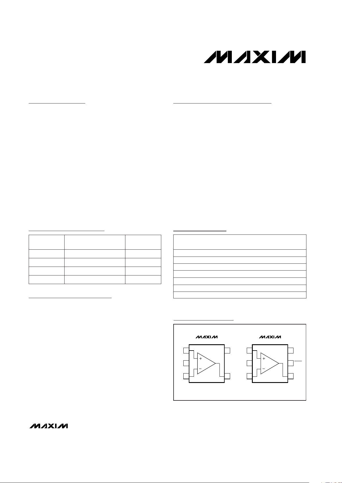
IN+
IN-
1
2
3
5
4
OUT
V
SS
VDDIN+
IN-
1
2
3
6
5
4
OUT
SHDN
V
SS
V
DD
MAX4400 MAX4401
SC70-5/SOT23-5 SC70-6
19-1599; Rev 0; 1/00
PART
MAX4400AXK-T
MAX4400AUK-T
MAX4401AXT-T
-40°C to +125°C
-40°C to +125°C
-40°C to +125°C
TEMP. RANGE
PIN-
PACKAGE
5 SC70-5
5 SOT23-5
6 SC70-6
*Future product—contact factory for availability.
Pin Configurations
Ordering Information
Selector Guide
MAX4402AKA-T*
MAX4402ASA*
MAX4403AUD*
-40°C to +125°C
-40°C to +125°C
-40°C to +125°C 8 SOT23-8
8 SO
14 TSSOP
MAX4403ASD* -40°C to +125°C 14 SO
MAX4401 1 Yes
MAX4402 2 No
MAX4403 4 No
Rail-to-Rail is a registered trademark of Nippon Motorola, Ltd.
Pin Configurations continued at end of data sheet.
No1MAX4400
PART
NO. OF AMPLIFIERS
PER PACKAGE
SHUTDOWN
MODE
TOP
MARK
AAG
ADNP
AAB
AADI
—
—
—

MAX4400–MAX4403
Single/Dual/Quad, Low-Cost, Single-Supply,
Rail-to-Rail Op Amps with Shutdown
2 _______________________________________________________________________________________
ABSOLUTE MAXIMUM RATINGS
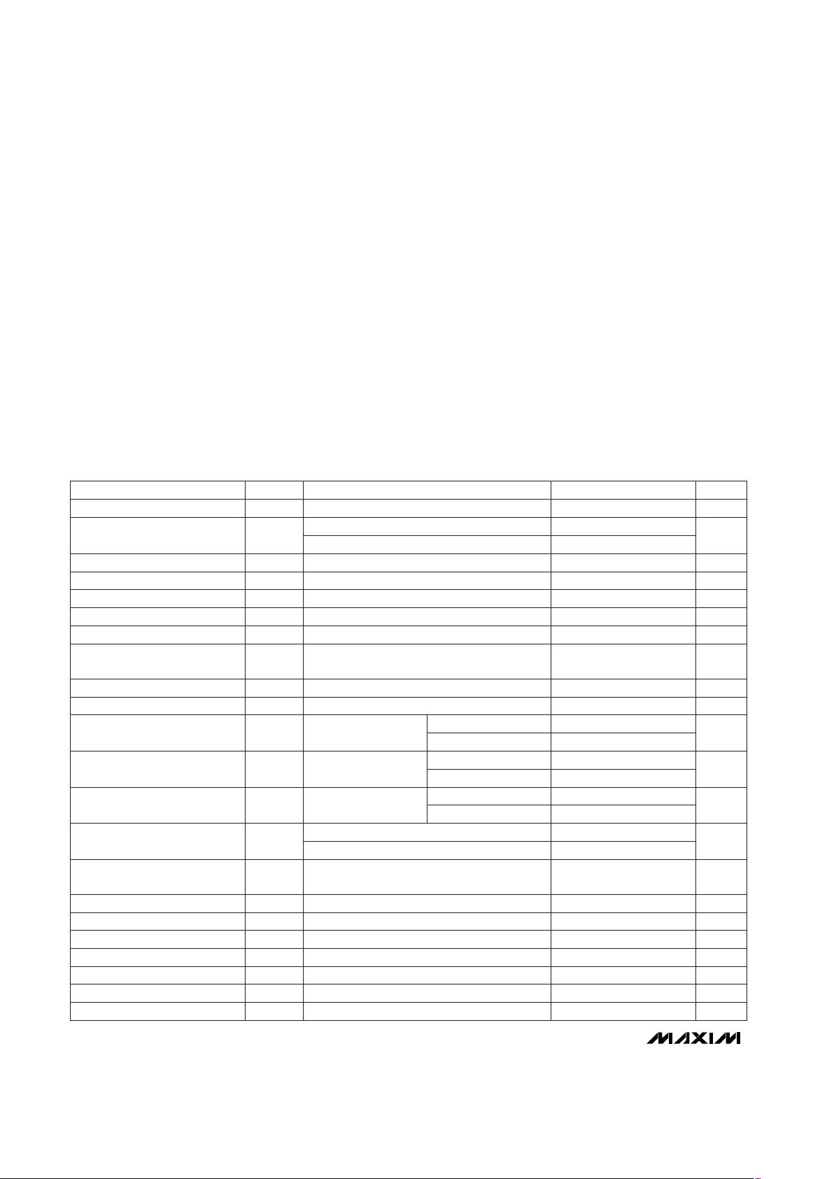
ELECTRICAL CHARACTERISTICS
(VDD= +5V, VSS= 0, VCM= 0, V
OUT
= VDD/2, RL= ∞ connected to VDD/2, SHDN = VDD(MAX4401 only), TA= +25°C, unless
otherwise noted.)
Stresses beyond those listed under “Absolute Maximum Ratings” may cause permanent damage to the device. These are stress ratings only, and functional
operation of the device at these or any other conditions beyond those indicated in the operational sections of the specifications is not implied. Exposure to
absolute maximum rating conditions for extended periods may affect device reliability.
Power-Supply Voltage (VDDto VSS) .........................-0.3V to +6V
All Other Pins ...................................(VSS- 0.3V) to (VDD+ 0.3V)
Output Short-Circuit Duration
(OUT shorted to VSSor VDD)................................. Continuous
Continuous Power Dissipation (TA= +70°C)
5-Pin SC70 (derate 2.5mW/°C above +70°C)............. 200mW
6-Pin SC70 (derate 2.27mW/°C above +70°C)............181mW
5-Pin SOT23 (derate 7.1mW/°C above +70°C)............571mW
8-Pin SOT23 (derate 7.52mW/°C above +70°C)..........602mW
8-Pin SO (derate 5.88mW/°C above +70°C)............... 471mW
14-Pin TSSOP (derate 8.33mW/°C above +70°C) ...... 667mW
14-Pin SO (derate 8.33mW/°C above +70°C)............. 667mW
Operating Temperature Range .........................-40°C to +125°C
Storage Temperature Range .............................-65°C to +150°C
Lead Temperature (soldering, 10s) .................................+300°C
SHDN = VDDor VSS(Notes 1, 2)
(Note 1)
VDD= 5.0V
(Note 1)
Device in shutdown mode, SHDN = VSS,
V
SS
< V
OUT
< VCC(Note 1)
V
DD
= 2.5V
Sinking
Inferred from PSRR test
Sourcing
Specified as
|VSS- VOL|
2.5V ≤ VDD≤ 5.5V
VSS≤ VCM≤ VDD- 1.4V
Specified as
|V
DD
- VOH|
Inferred from CMRR test
Differential or common mode
SHDN = VSS(Note 1)
(Note 2)
dB
(Note 2)
VSS+ 0.3V ≤
V
OUT
≤ VDD- 0.3V
CONDITIONS
kHz
800
GBWGain-Bandwidth Product
pA
±1 ±100
IIL, I
IH
SHDN Input Current
V
0.7 · V
DD
V
IH
SHDN Logic High
V
0.3 · V
DD
V
IL
SHDN Logic Low
µA
±1.0
I
OUTSHDN
Shutdown Mode Output
Leakage
30
mA
12
Output Short-Circuit Current
30 75
mV
2
V
OL
Output Voltage Low
55 200
mV
3
V
OH
Output Voltage High
90 110
dB
120
A
VOL
Large-Signal Voltage Gain
400 700
RL= 100kΩ
RL= 2kΩ
µA
320
I
DD
V
2.5 5.5
V
DD
Supply Voltage Range
Supply Current per Amplifier
78 100
PSRRPower-Supply Rejection Ratio
dB
68 84
CMRRCommon-Mode Rejection Ratio
V
V
SS
VDD- 1.4
V
CM
Input Common-Mode Voltage
Range
GΩ
1000
R
IN
Input Resistance
µA
0.00002 1
I
SHDN
Supply Current in Shutdown
mV
±0.8 ±4.5
V
OS
Input Offset Voltage
pA
±0.1 ±100
I
B
Input Bias Current
pA
±0.1 ±100
I
OS
Input Offset Current
UNITSMIN TYP MAXSYMBOLPARAMETER
RL= 100kΩ
RL= 2kΩ
RL= 100kΩ
RL= 2kΩ
degrees
70
φ
M
Phase Margin
dB
20
Gain Margin
V/µs
1
SRSlew Rate

MAX4400–MAX4403
Single/Dual/Quad, Low-Cost, Single-Supply,
Rail-to-Rail Op Amps with Shutdown
_______________________________________________________________________________________ 3
Total Harmonic Distortion
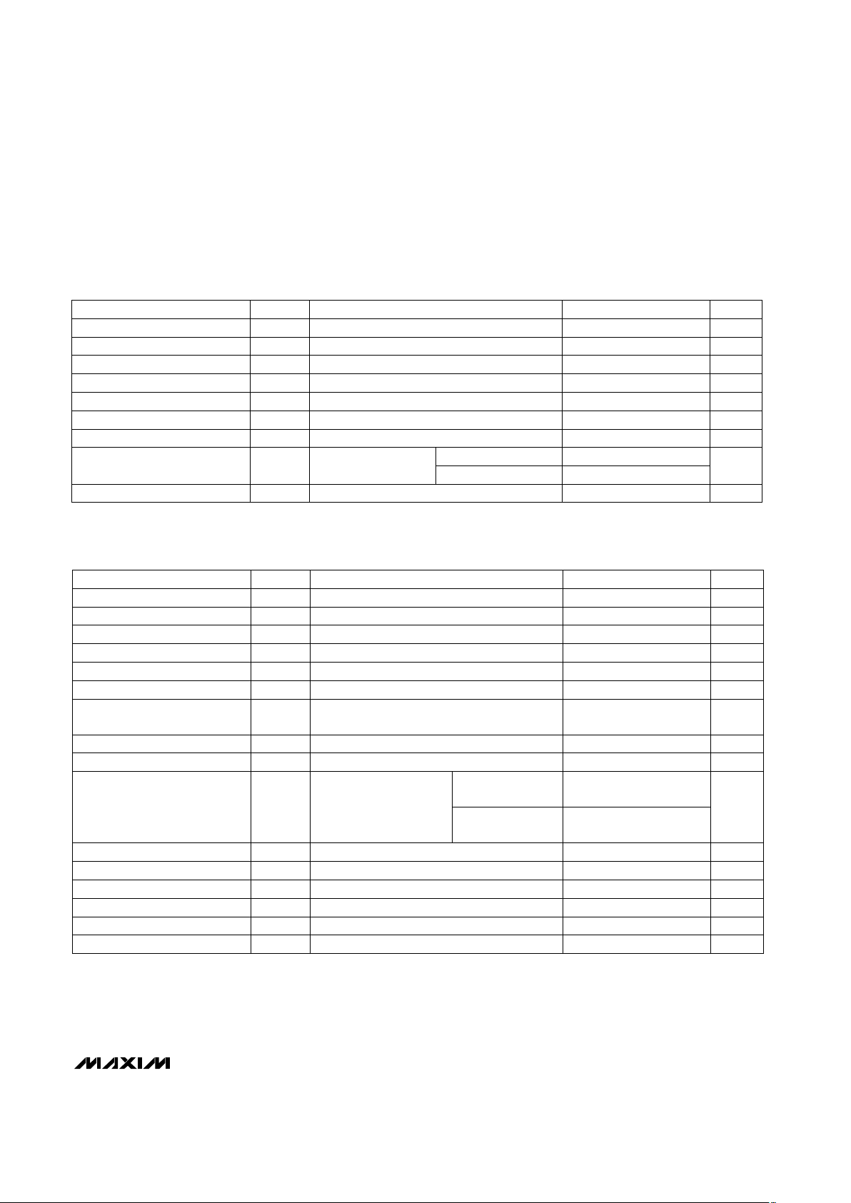
ELECTRICAL CHARACTERISTICS (continued)
(VDD= +5V, VSS= 0, VCM= 0, V
OUT
= VDD/2, RL= ∞ connected to VDD/2, SHDN = VDD(MAX4401 only), TA= +25°C, unless
otherwise noted.)
ELECTRICAL CHARACTERISTICS
(VDD= +5V, VSS= 0, VCM= 0, V
OUT
= VDD/2, RL= ∞ connected to VDD/2, TA= -40°C to +125°C, unless otherwise noted.) (Note 3)
Note 1: Shutdown mode is only available in the 6-pin SC70 single op amp (MAX4401).
Note 2: Guaranteed by design.
Note 3: Specifications are 100% tested at T
A
= +25°C (exceptions noted). All temperature limits are guaranteed by design.
RL= 100kΩ
RL= 2kΩ
CONDITIONS UNITSMIN TYP MAXSYMBOLPARAMETER
V
OUT
= 2V step
(Note 1)
AV= 1V/V
f = 10kHz, V
OUT
=
2Vp-p, AV= 1V/V
f = 10kHz
f = 10kHz
(Note 1)
µs
7
t
S
Settling Time to 0.1%
0.015
%
0.009
THDTotal Harmonic Distortion
pF
2.5
C
IN
Input Capacitance
µs
5
t
ON
Power-On Time
µs
6
t
EN
Enable Delay Time
µs
0.4
t
SHDN
Shutdown Delay Time
pF
400
C
LOAD
Capacitive-Load Stability
fA/√Hz
1
i
n
Input Current Noise Density
nV/√Hz
36e
n
Input Voltage Noise Density
+85°C to +125°C
-40°C to +85°C
±5.0
Device in shutdown
mode, SHDN = V
SS
,
V
SS
< V
OUT
< V
DD
(Note 1)
Inferred from PSRR test
Specified as |VSS- VOL|, RL = 2kΩ
Specified as |VDD- VOH|, RL= 2kΩ
VSS+ 0.3V ≤ V
OUT
≤ VDD- 0.3V, RL= 2kΩ
SHDN = VDDor VSS(Notes 1, 2)
(Note 1)
2.5V ≤ VCC≤ 5.5V
V
SS
≤ VCM≤ VDD- 1.5V
(Note 2)
(Note 2)
(Note 1)
Inferred from CMRR test
CONDITIONS
mV
100
V
OL
Output Voltage Low
mV
250
V
OH
Output Voltage High
dB
85
A
VOL
Large-Signal Voltage Gain
pA
±100
I
IL,IIH
SHDN Input Current
V
0.7 · V
DD
V
IH
SHDN Logic High
V
0.3 · V
DD
V
IL
SHDN Logic Low
mV
±6.5
V
OS
Input Offset Voltage
µA
800
I
DD
V
2.5 5.5
V
DD
Supply Voltage Range
Supply Current per Amplifier
µA
±1.0
I
OUTSHDN
Shutdown Mode Output
Leakage
dB
74
PSRRPower-Supply Rejection Ratio
dB
65
CMRRCommon-Mode Rejection Ratio
µV/°C
±1
TC
VOS
Input Offset Voltage Drift
pA
±100
I
B
Input Bias Current
pA
±100
I
OS
Input Offset Current
V
V
SS
V
DD
- 1.5
V
CM
Input Common-Mode Voltage
Range
UNITSMIN TYP MAXSYMBOLPARAMETER

MAX4400–MAX4403
Single/Dual/Quad, Low-Cost, Single-Supply,
Rail-to-Rail Op Amps with Shutdown
4 _______________________________________________________________________________________
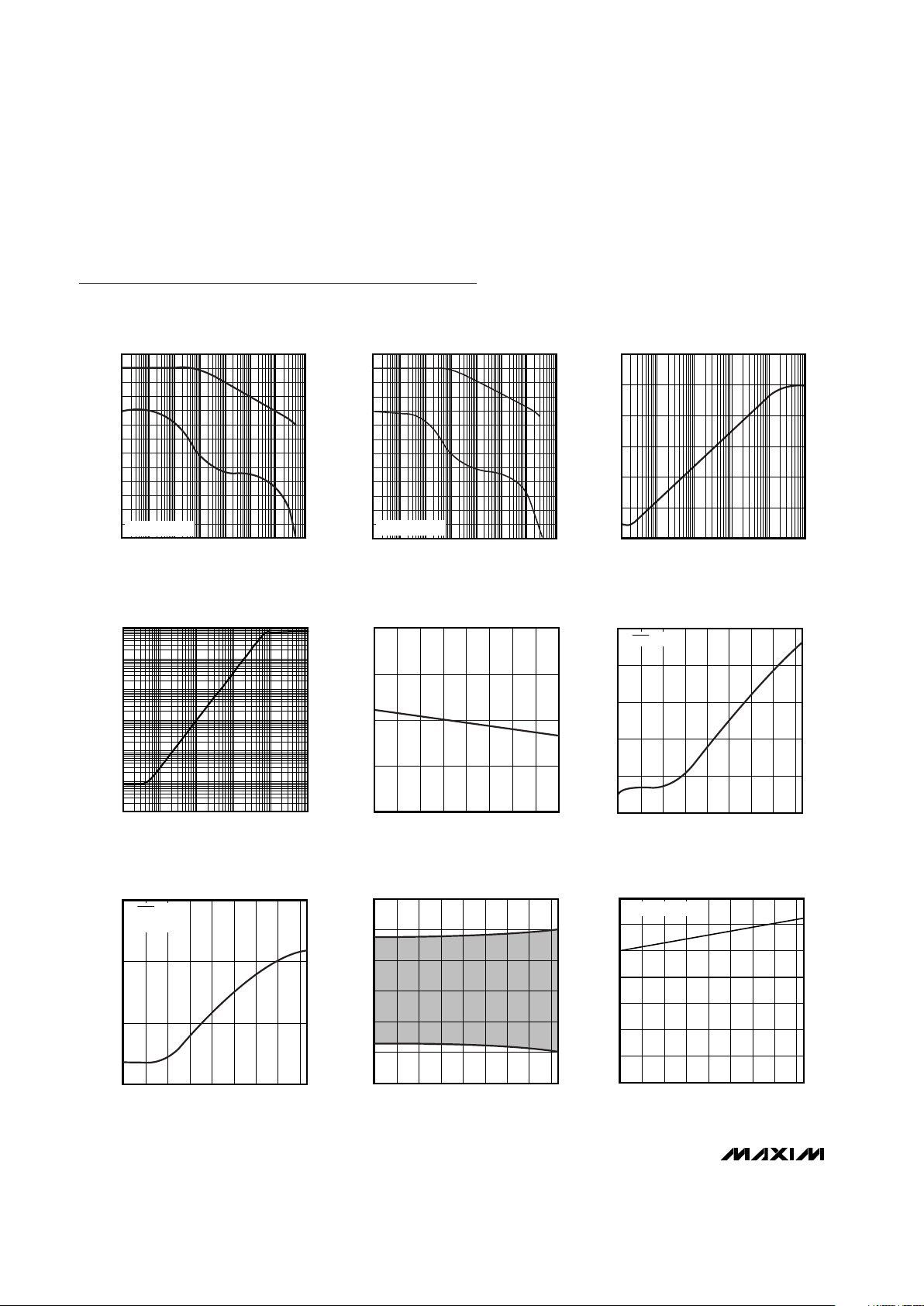
Typical Operating Characteristics
(VDD= +5V, VSS= 0, VCM= VDD/2, V
SHDN
= 5V, RL= ∞ connected to VDD/2, TA= +25°C, unless otherwise noted.)
80
60
40
20
0
-20
-40
-60
-80
-100
-120
-140
-160
-180
1 10 1k 10M1M
GAIN AND PHASE
vs. FREQUENCY (NO LOAD)
MAX4400 toc01
FREQUENCY (Hz)
GAIN (dB)/PHASE (deg)
100 10k 100k
A
VCL
= +1000V/V
80
60
40
20
0
-20
-40
-60
-80
-100
-120
-140
-160
-180
1 10 1k 10M1M
GAIN AND PHASE vs. FREQUENCY
(C
L
= 400pF)
MAX4400 toc02
FREQUENCY (Hz)
GAIN (dB)/PHASE (deg)
100 10k 100k
A
VCL
= +1000V/V
10 1k100 10k 100k 1M
POWER-SUPPLY REJECTION RATIO
vs. FREQUENCY
MAX4400 toc03
FREQUENCY (Hz)
PSRR (dB)
10
-110
-90
-10
-30
-50
-70
FREQUENCY (Hz)
1000
0.001
10 100 1k 10k 100k 1M
OUTPUT IMPEDANCE
vs. FREQUENCY
0.1
MAX4400 toc4
OUTPUT IMPEDANCE (Ω)
10
0.01
1
100
300
350
400
450
500
-40 0 40 80-20 20 60 100 120
SUPPLY CURRENT vs. TEMPERATURE
MAX4400 toc05
TEMPERATURE (°C)
SUPPLY CURRENT (µA)
1
10
100
1k
10k
1M
-40 0 40 80-20 20 60 100 120
MAX4401
SHUTDOWN SUPPLY CURRENT
vs. TEMPERATURE
MAX4400 toc06
TEMPERATURE (°C)
SUPPLY CURRENT (pA)
V
SHDN
= V
SS
0.1
10
1k
1M
-40 0 40 80-20 20 60 100 120
MAX4401
OUTPUT LEAKAGE CURRENT
vs. TEMPERATURE
MAX4400 toc07
TEMPERATURE (°C)
I
LEAK
(pA)
V
SHDN
= V
SS
V
OUT = VDD/2
-1500
-1000
-500
500
0
1000
1500
-40 0 40 80-20 20 60 100 120
INPUT OFFSET VOLTAGE
vs. TEMPERATURE
MAX4400 toc08
TEMPERATURE (°C)
V
OS
(µV)
30
20
10
0
50
40
70
60
-40 0 40 80-20 20 60 100 120
OUTPUT VOLTAGE SWING HIGH
vs. TEMPERATURE
MAX4400 toc09
TEMPERATURE (°C)
V
DD
-V
OH
(mV)
RL = 2kΩ to VDD/2
 Loading...