

Page 1
General Description
The MAX4389/MAX4390/MAX4392–MAX4396 family of
op amps are unity-gain stable devices that combine
high-speed performance, rail-to-rail outputs, and disable mode. These devices are targeted for applications
where an input or an output is exposed to the outside
world, such as video and communications.
The MAX4389/MAX4390/MAX4392–MAX4396 operate
from a single 4.5V to 11V supply or from dual ±2.25V to
±5.5V supplies. The common-mode input voltage range
extends to the negative power-supply rail (ground in single-supply applications). The MAX4389/MAX4390/
MAX4392–MAX4396 consume only 5.5mA of quinescent
supply current per amplifier while achieving a 85MHz
-3dB bandwidth, 27MHz 0.1dB gain flatness, and a
500V/µs slew rate. Disable mode sets the outputs to high
impedance while consuming only 450µA of current.
The MAX4389 single, MAX4393 dual, MAX4394 triple,
and MAX4396 quad include disable capabilities. The
MAX4389 and MAX4390 are available in ultra-small,
6-pin SC70 packages.
Applications
Set-Top Boxes
Surveillance Video Systems
Analog-to-Digital Converter Interface
CCD Imaging Systems
Digital Cameras
Video-on-Demand
Video Line Driver
Features
♦ Low Cost
♦ High Speed
85MHz -3dB Bandwidth
27MHz 0.1dB Gain Flatness
500V/µs Slew Rate
♦ Single 4.5V to 11V or Dual ±2.25V to ±5.5V
Operation
♦ Rail-to-Rail Outputs
♦ Input Common-Mode Range Extends to V
EE
♦ Low Differential Gain/Phase: 0.015%/0.015°
♦ Low Distortion at 5MHz
-59dBc Spurious-Free Dynamic Range
♦ High Output Drive: ±50mA
♦ 450µA Disable Capability
(MAX4389/MAX4393/MAX4394/MAX4396)
♦ Space-Saving SC70, SOT23, µMAX, or TSSOP
Packages
MAX4389/MAX4390/MAX4392–MAX4396
Ultra-Small, Low-Cost, 85MHz Op Amps with
Rail-to-Rail Outputs and Disable
________________________________________________________________
Maxim Integrated Products
1
Pin Configurations
19-2322; Rev 4; 11/09
For pricing, delivery, and ordering information, please contact Maxim Direct at 1-888-629-4642,
or visit Maxim’s website at www.maxim-ic.com.
Ordering Information
Pin Configurations continued at end of data sheet.
200Ω
200Ω
75Ω
75Ω
IN
OUT
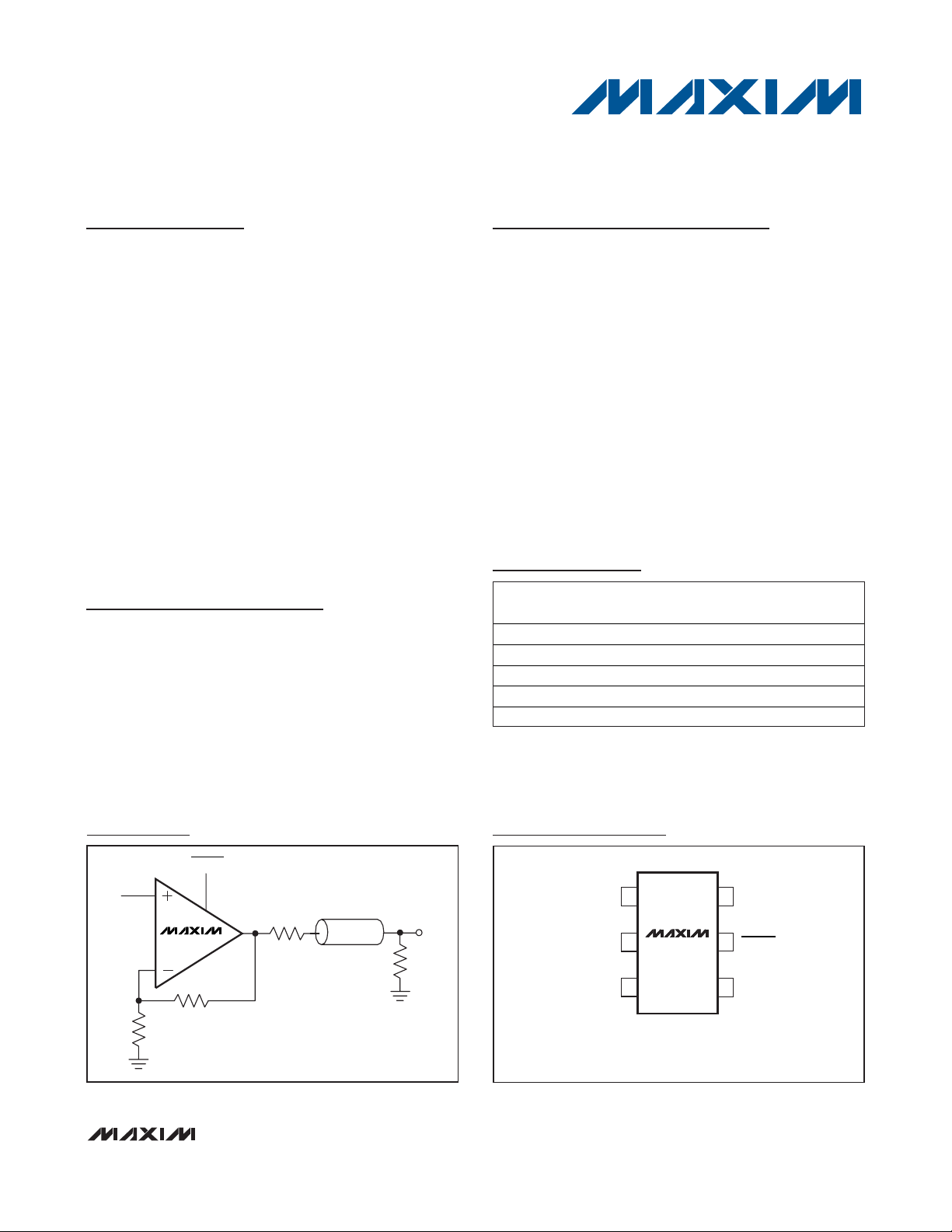
VIDEO LINE DRIVER
Z
o
= 75Ω
DISABLE
MAX4389
Typical Operating Circuit
Ordering Information continued at end of data sheet.
Selector Guide appears at end of data sheet.
+
Denotes a lead(Pb)-free/RoHs-compliant package.
/V denotes an automotive qualified part.
T = Tape and reel.
PART TEMP RANGE
MAX4389EXT+T -40°C to +85°C 6 SC70 ABF
MAX4389EUT+T -40°C to +85°C 6 SOT23 ABDC
MAX4389EUT/V+T -40°C to +85°C 6 SOT23 ABDC
MAX4390EXT+T -40°C to +85°C 6 SC70 ABE
MAX4390EUK+T -40°C to +85°C 5 SOT23 ADZM
PINPACKAGE
TOP
MARK
TOP VIEW
+
16V
OUT
V
2
EE
MAX4389
34
SC70/SOT23
CC
5 DISABLE
IN-IN+
Page 2
MAX4389/MAX4390/MAX4392–MAX4396
Ultra-Small, Low-Cost, 85MHz Op Amps with
Rail-to-Rail Outputs and Disable
2 _______________________________________________________________________________________
ABSOLUTE MAXIMUM RATINGS
Stresses beyond those listed under “Absolute Maximum Ratings” may cause permanent damage to the device. These are stress ratings only, and functional
operation of the device at these or any other conditions beyond those indicated in the operational sections of the specifications is not implied. Exposure to
absolute maximum rating conditions for extended periods may affect device reliability.
Supply Voltage (VCCto VEE) ..................................-0.3V to +12V
IN_+, IN_-, OUT_, DISABLE.............(V
EE
- 0.3V) to (VCC+ 0.3V)
Differential Input Voltage ....................................................±2.5V
Current into Input Pins ......................................................±20mA
Output Short-Circuit Duration to
V
CC
or VEE(Note 1)................................................Continuous
Continuous Power Dissipation (T
A
= +70°C)
5-Pin SOT23 (derate 7.1mW/°C above +70°C)............571mW
6-Pin SOT23 (derate 8.7mW/°C above +70°C)............696mW
6-Pin SC70 (derate 3.1mW/°C above +70°C)..............245mW
8-Pin SO (derate 5.88mW/°C above +70°C)................471mW
8-Pin µMAX (derate 4.5mW/°C above +70°C) .............362mW
10-Pin µMAX (derate 5.6mW/°C above +70°C) ...........444mW
14-Pin SO (derate 8.33mW/°C above +70°C)..............667mW
14-Pin TSSOP (derate 10mW/°C above +70°C) ..........727mW
20-Pin TSSOP (derate 10.9mW/°C above +70°C) .......879mW
Operating Temperature Range ...........................-40°C to +85°C
Junction Temperature......................................................+150°C
Storage Temperature Range .............................-65°C to +150°C
Lead Temperature (soldering, 10s) .................................+300°C
DC ELECTRICAL CHARACTERISTICS—Single Supply
(VCC= 5V, VEE= 0V, VCM= VCC/2, V
OUT
= VCC/2, RL= ∞ to VCC/2, DISABLE_ = VCC(MAX4389/MAX4393/MAX4394/MAX4396),
T
A
= T
MIN
to T
MAX
, unless otherwise noted. Typical values are at TA= +25°C.) (Note 2)
Note 1: Continuous power dissipation must also be observed.
PARAMETER SYMBOL CONDITIONS MIN TYP MAX UNITS
Input Common-Mode Voltage
Range
Input Offset Voltage V
Input Offset Voltage Matching MAX4392–MAX4396 1 mV
Input Offset Voltage Tempco TC
Input Bias Current I
Input Offset Current I
Input Resistance R
Common-Mode Rejection Ratio CMRR (VEE - 0.2V) ≤ VCM ≤ (VCC - 2.25V) 70 95 dB
Open-Loop Gain A
Output Voltage Swing V
Output Current I
Output Short-Circuit Current I
Open-Loop Output Resistance R
V
CM
OS
VOS
B
Guaranteed by CMRR test
TA = +25°C 5 18
TA = -40°C to +85°C 26
OS
IN
VOL
Differential mode (-1V ≤ VIN ≤ +1V) 70 kΩ
Common mode (-0.2V ≤ VCM ≤ +2.75V) 3 MΩ
0.25V ≤ V
0.8V ≤ V
1V ≤ V
OUT
≤ 4.5V, R
OUT
≤ 4V, RL = 50Ω 58
OUT
RL = 2kΩ
RL = 150Ω
OUT
RL = 75Ω
RL = 75Ω to
ground
OUT
SC
OUT
Sinking from RL = 75Ω to V
Sourcing into RL = 75Ω to V
Sinking or sourcing ±100 mA
V
EE
0.2
-
VCC -
2.25
15 µV/°C
2.5 15 µA
0.2 5 µA
≤ 4.75V, R
= 2kΩ 50 70
L
= 150Ω 50 60
L
VCC - V
OH
V
- V
OL
EE
VCC - V
OH
V
- V
OL
EE
V
- V
CC
OH
V
- V
OL
EE
VCC - V
OH
- V
V
OL
EE
CC
EE
40 55
40 50
0.065 0.25
0.05 0.15
0.3 0.5
0.25 0.5
0.5 0.8
0.45 0.8
1 1.7
0.025 0.1
8 Ω
V
mV
dB
V
mA
Page 3
MAX4389/MAX4390/MAX4392–MAX4396
Ultra-Small, Low-Cost, 85MHz Op Amps with
Rail-to-Rail Outputs and Disable
_______________________________________________________________________________________ 3
DC ELECTRICAL CHARACTERISTICS—Dual Supply
(VCC= 5V, VEE= -5V, VCM= 0V, V
OUT
= 0V, RL= ∞ to 0, DISABLE_ = VCC(MAX4389/MAX4393/MAX4394/MAX4396),
T
A
= T
MIN
to T
MAX
, unless otherwise noted. Typical values are at TA= +25°C.) (Note 2)
DC ELECTRICAL CHARACTERISTICS—Single Supply (continued)
(VCC= 5V, VEE= 0V, VCM= VCC/2, V
OUT
= VCC/2, RL= ∞ to VCC/2, DISABLE_ = VCC(MAX4389/MAX4393/MAX4394/MAX4396),
T
A
= T
MIN
to T
MAX
, unless otherwise noted. Typical values are at TA= +25°C.) (Note 2)
)
Power-Supply Rejection Ratio PSRR VEE = 0V, V
Operating Supply Voltage
Range
Disabled Output Resistance R
DISABLE_ Logic-Low Threshold V
DISABLE_ Logic-High Threshold V
DISABLE_ Logic Input Low
Current
DISABLE_ Logic Input High
Current
Quiescent Supply Current
(Per Amplifier)
PARAMETER SYMBOL CONDITIONS MIN TYP MAX UNITS
= 4.5V to 5.5V 48 65 dB
CC
V
OUT(OFF
IL
IH
I
IL
I
IH
I
S
Guaranteed by PSRR 4.5 11 V
S
DISABLE_ = 0, 0 ≤ V
DISABLE_ = 0 20 60 µA
DISABLE_ = V
DISABLE_ = V
DISABLE_ = 0 0.3 0.4
CC
CC
≤ 5V 40 95 kΩ
OUT
VCC -
1.25
V
- 3V
CC
V
540µA
3.2 5
mA
Input Common-Mode Voltage
Input Offset Voltage V
Input Offset Voltage Matching MAX4392–MAX4396 1 mV
Input Offset Voltage Tempco TC
Input Bias Current I
Input Offset Current I
Input Resistance R
Common-Mode Rejection
Ratio
Open-Loop Gain A
PARAMETER SYMBOL CONDITIONS MIN TYP MAX UNITS
V
CM
OS
VOS
B
OS
IN
CMRR V
VOL
Guaranteed by CMRR test V
TA = +25°C 7 20
TA = -40°C to +85°C 28
Differential mode (-1V ≤ VIN ≤ +1V) 70 kΩ
Common mode (-0.2V ≤ VCM ≤ +2.75V) 3 MΩ
≤ VCM ≤ (VCC - 2.25V) 70 90 dB
EE
-4.5V ≤ V
-4.25V ≤ V
≤ 4.5V, RL = 2kΩ 65 80
OUT
≤ 4.25V, RL = 150Ω 50 60
OUT
EE
VCC - 2.25 V
20 µV/°C
515µA
0.5 5 µA
mV
dB
Page 4
MAX4389/MAX4390/MAX4392–MAX4396
Ultra-Small, Low-Cost, 85MHz Op Amps with
Rail-to-Rail Outputs and Disable
4 _______________________________________________________________________________________
AC ELECTRICAL CHARACTERISTICS—Single Supply
(VCC= 5V, VEE= 0V, VCM= 1.5V, RL= 100Ω to VCC/2, DISABLE_ = VCC(MAX4389/MAX4393/MAX4394/MAX4396),
V
OUT
= VCC/2, A
VCL
= 1V/V, TA= +25°C, unless otherwise noted.)
DC ELECTRICAL CHARACTERISTICS—Dual Supply (continued)
(VCC= 5V, VEE= -5V, VCM= 0V, V
OUT
= 0V, RL= ∞ to 0, DISABLE_ = VCC(MAX4389/MAX4393/MAX4394/MAX4396),
T
A
= T
MIN
to T
MAX
, unless otherwise noted. Typical values are at TA= +25°C.) (Note 2)
)
PARAMETER SYMBOL CONDITIONS MIN TYP MAX UNITS
Output Voltage Swing V
Output Current I
Output Short-Circuit Current I
Open-Loop Output Resistance R
Power-Supply Rejection Ratio PSRR VEE = 0V, V
Operating Supply Voltage
Range
Disabled Output Resistance R
DISABLE_ Logic-Low Threshold V
DISABLE_ Logic-High Threshold V
Quiescent Supply Current
(Per Amplifier)
OUT
OUT
SC
OUT
V
S
OUT(OFF
IL
IH
I
S
VCC - V
RL = 2kΩ
RL = 150Ω
RL = 75Ω
Sinking from RL = 75Ω to V
Sourcing into RL = 75Ω to V
V
- V
OL
VCC - V
V
- V
OL
VCC - V
V
- V
OL
OH
EE
OH
EE
OH
EE
CC
EE
Sinking or sourcing ±100 mA
= 4.5V to 5.5V 48 60 dB
CC
Guaranteed by PSRR 4.5 11 V
DISABLE_ = 0V, -5V ≤ V
≤ +5V 40 95 kΩ
OUT
VCC - 1.25 V
DISABLE_ = V
CC
DISABLE_ = 0V 0.45 0.8
0.175 0.3
0.075 0.2
0.575 0.85
0.4 1.5
1.5 2.35
0.75 1.6
50 95
50 75
8 Ω
V CC - 3V
610
V
mA
mA
PARAMETER SYMBOL CONDITIONS MIN TYP MAX UNITS
Small-Signal -3dB Bandwidth BW
Large-Signal -3dB Bandwidth BW
Small-Signal 0.1dB Gain
Flatness
Large-Signal 0.1dB Gain
Flatness
Slew Rate SR V
Settling Time to 0.1% t
Rise/Fall Time tR/t
Spurious-Free Dynamic Range SFDR f
V
SS
LS
BW
0.1dBSSVOUT
BW
0.1dBLSVOUT
s
F
OUT
V
OUT
OUT
V
OUT
V
OUT
= 5MHz, V
C
= 100mV
= 2V
P-P
= 100mV
= 2V
P-P
P-P
P-P
72 MHz
80 MHz
30 MHz
30 MHz
= 2V step 500 V/µs
= 2V step 28 ns
= 100mV
P-P
OUT
= 2V
P-P
4ns
-59 dBc
Page 5
MAX4389/MAX4390/MAX4392–MAX4396
Ultra-Small, Low-Cost, 85MHz Op Amps with
Rail-to-Rail Outputs and Disable
_______________________________________________________________________________________ 5
Note 2: All devices are 100% production tested at TA= +25°C. Specifications over temperature limits are guaranteed by design.
AC ELECTRICAL CHARACTERISTICS—Dual Supply
(VCC= 5V, VEE= -5V, RL= ∞ to GND, GND = 0, V
OUT
= 0V, Gain = 1V/V, DISABLE = VCC, and TA= T
MIN
to T
MAX
, unless otherwise
noted. Typical values are at T
A
= +25°C.)
AC ELECTRICAL CHARACTERISTICS—Single Supply (continued)
(VCC= 5V, VEE= 0V, VCM= 1.5V, RL= 100Ω to VCC/2, DISABLE_ = VCC(MAX4389/MAX4393/MAX4394/MAX4396),
V
OUT
= VCC/2, A
VCL
= 1V/V, TA= +25°C, unless otherwise noted.)
PARAMETER SYMBOL CONDITIONS MIN TYP MAX UNITS
Differential Phase Error DP NTSC, RL = 150Ω 0.015 degrees
Differential Gain Error DG NTSC, RL = 150Ω 0.015 %
Input Noise-Voltage Density e
Input Noise-Current Density i
Input Capacitance C
Output Impedance Z
n
OUT
f = 10kHz 13 nV/√Hz
n
f = 10kHz 2.1 pA/√Hz
IN
1pF
f = 5MHz 0.6 Ω
Disable OFF Time MAX4389/MAX4393/MAX4394/MAX4396 80 ns
Disable ON Time MAX4389/MAX4393/MAX4394/MAX4396 40 ns
Channel-to-Channel Isolation CH
MAX4392–MAX4396, specified at DC -97 dB
ISO
PARAMETER SYMBOL CONDITIONS MIN TYP MAX UNITS
Small-Signal -3dB Bandwidth BW
Large-Signal -3dB Bandwidth BW
Small-Signal Bandwidth for
0.1dB Gain Flatness
Large-Signal Bandwidth for
0.1dB Gain Flatness
SS
LS
BW
0.1dBssVOUT
BW
0 .1 d B LS VOUT
Slew Rate SR V
Settling Time to 0.1% t
Rise/Fall Time tR/t
S
F
Spurious-Free Dynamic Range SFDR f
Differential Phase Error DP NTSC, R
Differential Gain Error DG NTSC, R
Input Noise-Voltage Density e
Input Noise-Current Density i
Input Capacitance C
Output Impedance Z
n
n
IN
OUT
Disable OFF Time MAX4389/MAX4393/MAX4394/MAX4396 80 ns
Disable ON Time MAX4389/MAX4393/MAX4394/MAX4396 40 ns
Channel-to-Channel Isolation CH
ISO
V
= 100mV
OUT
V
= 2V
OUT
= 100mV
= 2V
= 2V step 500 V/µs
OUT
V
= 2V step 21 ns
OUT
V
= 100mV
OUT
= 5MHz, V
C
P-P
P-P
P-P
P-P
P-P
= 2V
OUT
= 150Ω 0.015 d eg r ees
L
= 150Ω 0.015 %
L
P-P
85 MHz
90 MHz
27 MHz
24 MHz
4ns
-59 dBc
f = 10kHz 13 nV/√Hz
f = 10kHz 2.1 pA/√Hz
1pF
f = 5MHz 0.6 Ω
MAX4392/MAX4393/MAX4394/MAX4395/
MAX4396, specified at DC
-97 dB
Page 6
GAIN AND PHASE
vs. FREQUENCY
MAX4389 toc01
FREQUENCY (Hz)
GAIN (dB)
100M1M 10M10k 100k
-100
-80
-60
-40
-20
0
20
40
60
80
-120
PHASE (DEGREES)
-225
-180
-135
-90
-45
0
45
90
135
180
-270
1k 1G
GAIN
PHASE
SMALL-SIGNAL GAIN
vs. FREQUENCY
MAX4389 toc02
FREQUENCY (Hz)
GAIN (dB)
100M10M1M
-5
-4
-3
-2
-1
0
1
2
3
4
-6
100k 1G
V
OUT
= 100mV
P-P
LARGE-SIGNAL GAIN
vs. FREQUENCY
MAX4389 toc03
FREQUENCY (Hz)
GAIN (dB)
100M10M1M
-5
-4
-3
-2
-1
0
1
2
3
4
-6
100k 1G
V
OUT
= 2V
P-P
SMALL-SIGNAL GAIN
FLATNESS vs. FREQUENCY
MAX4389 toc04
FREQUENCY (Hz)
GAIN (dB)
100M10M1M
-0.5
-0.4
-0.3
-0.2
-0.1
0
0.1
0.2
0.3
0.4
-0.6
100k 1G
V
OUT
= 100mV
P-P
DISTORTION vs. FREQUENCY
MAX4389 toc07
FREQUENCY (Hz)
DISTORTION (dBc)
10M1M
-80
-90
-70
-60
-50
-40
-30
-20
-10
0
-100
100k 100M
V
OUT
= 2V
P-P
, A
VCL
= 1V/V
2ND HARMONIC
3RD HARMONIC
LARGE-SIGNAL GAIN
FLATNESS vs. FREQUENCY
MAX4389 toc05
FREQUENCY (Hz)
GAIN (dB)
100M10M1M
-0.5
-0.4
-0.3
-0.2
-0.1
0
0.1
0.2
0.3
0.4
-0.6
100k 1G
V
OUT
= 2V
P-P
OUTPUT IMPEDANCE vs. FREQUENCY
MAX4389 toc06
FREQUENCY (Hz)
OUTPUT IMPEDANCE (Ω)
100M10M1M
0.1
1
10
100
0.01
100k 1G
DISTORTION vs. FREQUENCY
MAX4389 toc08
FREQUENCY (Hz)
DISTORTION (dBc)
10M1M
-80
-90
-70
-60
-50
-40
-30
-20
-10
0
-100
100k 100M
V
OUT
= 2V
P-P
, A
VCL
= 2V/V
2ND HARMONIC
3RD HARMONIC
DISTORTION vs. FREQUENCY
MAX4389 toc09
FREQUENCY (Hz)
DISTORTION (dBc)
10M1M
-80
-90
-70
-60
-50
-40
-30
-20
-10
0
-100
100k 100M
V
OUT
= 2V
P-P
, A
VCL
= 5V/V
3RD HARMONIC
2ND HARMONIC
Typical Operating Characteristics
(VCC= 5V, VEE= -5V, VCM= 0V, A
VCL
= 1V/V, RL= 100Ω to GND, GND = 0, TA= +25°C, unless otherwise noted.)
MAX4389/MAX4390/MAX4392–MAX4396
Ultra-Small, Low-Cost, 85MHz Op Amps with
Rail-to-Rail Outputs and Disable
6 _______________________________________________________________________________________
Page 7
DISTORTION vs. RESISTIVE LOAD
MAX4389 toc10
VOLTAGE SWING (V
P-P
)
DISTORTION (dBc)
800 1000200 400 600
-80
-70
-60
-50
-40
-30
-20
-10
-90
0 1200
0
fo = 5MHz, V
OUT
= 2V
P-P
, A
VCL
= 1V/V
3RD HARMONIC
2ND HARMONIC
-100
DISTORTION vs. VOLTAGE SWING
MAX4389 toc11
VOLTAGE SWING (V
P-P
)
DISTORTION (dBc)
1.51.0
-90
-70
-80
-60
-50
-40
-30
-20
-10
-100
0.5 2.0
fo = 5MHz, A
VCL
= 1V/V
0
3RD HARMONIC
2ND HARMONIC
DIFFERENTIAL GAIN AND PHASE
MAX4389 toc12
IRE
DIFF GAIN (%)
2
3
45
1
DIFF PHASE (°)
-0.1
0
0.2
0.1
0.3
0.4
0.5
-0.5
-0.4
-0.2
-0.3
-0.1
0
0.1
06
RL = 150Ω TO GND, A
VCL
= 2V/V
RL = 150Ω TO GND, A
VCL
= 2V/V
COMMON-MODE REJECTION
vs. FREQUENCY
MAX4389 toc13
FREQUENCY (Hz)
GAIN (dB)
100M10M1M
-70
-60
-50
-40
-30
-20
-10
0
-80
100k 1G
SMALL-SIGNAL PULSE RESPONSE
MAX4389 toc16
20ns/div
INPUT
50mV/div
OUTPUT
50mV/div
A
VCL
= 1V/V
POWER-SUPPLY REJECTION
vs. FREQUENCY
MAX4389 toc14
FREQUENCY (Hz)
PSR (dB)
100M10M1M
-60
-50
-40
-30
-20
-10
0
-70
100k 1G
OUTPUT VOLTAGE SWING
vs. RESISTIVE LOAD
MAX4389 toc15
R
LOAD
(Ω)
OUTPUT VOLTAGE SWING (V)
500400100 200 300
0.2
0.4
0.6
0.8
1.0
1.2
1.4
1.6
0
0 600
V
CC
- V
OH
VOL- V
EE
SMALL-SIGNAL PULSE RESPONSE
MAX4389 toc17
20ns/div
INPUT
25mV/div
OUTPUT
50mV/div
A
VCL
= +2V/V
R
F
= 200Ω
A
VCL
= 2V/V
R
F
= 200Ω
SMALL-SIGNAL PULSE RESPONSE
MAX4389 toc18
20ns/div
INPUT
10mV/div
OUTPUT
50mV/div
A
VCL
= 5V/V
R
F
= 250Ω
Typical Operating Characteristics (continued)
(VCC= 5V, VEE= -5V, VCM= 0V, A
VCL
= 1V/V, RL= 100Ω to GND, GND = 0, TA= +25°C, unless otherwise noted.)
MAX4389/MAX4390/MAX4392–MAX4396
Ultra-Small, Low-Cost, 85MHz Op Amps with
Rail-to-Rail Outputs and Disable
_______________________________________________________________________________________
7
Page 8
LARGE-SIGNAL PULSE RESPONSE
MAX4389 toc19
20ns/div
INPUT
500mV/div
OUTPUT
500mV/div
A
VCL
= 1V/V
LARGE-SIGNAL PULSE RESPONSE
MAX4389 toc20
20ns/div
INPUT
250mV/div
OUTPUT
500mV/div
A
VCL
= 2V/V
R
F
= 200Ω
LARGE-SIGNAL PULSE RESPONSE
MAX4389 toc21
20ns/div
INPUT
100mV/div
OUTPUT
500mV/div
A
VCL
= 5V/V
R
F
= 250Ω
VOLTAGE NOISE vs. FREQUENCY
MAX4389 toc22
FREQUENCY (Hz)
VOLTAGE NOISE (nV/√Hz)
10k1k10010
10
100
1000
1
1 100k
RL = 100Ω
CURRENT NOISE vs. FREQUENCY
MAX4389 toc23
FREQUENCY (Hz)
CURRENT NOISE (pA/√Hz)
10k1k10010
10
100
1000
1
1 100k
RL = 100Ω
ISOLATION RESISTANCE
vs. CAPACITIVE LOAD
MAX4389 toc24
FREQUENCY (Hz)
GAIN (dB)
100M10M1M
-4
-3
-2
-1
0
1
3
4
5
6
-5
-6
100k 1G
100pF
68pF
33pF
2
Typical Operating Characteristics (continued)
(VCC= 5V, VEE= -5V, VCM= 0V, A
VCL
= 1V/V, RL= 100Ω to GND, GND = 0, TA= +25°C, unless otherwise noted.)
MAX4389/MAX4390/MAX4392–MAX4396
Ultra-Small, Low-Cost, 85MHz Op Amps with
Rail-to-Rail Outputs and Disable
8 _______________________________________________________________________________________
Page 9

SMALL-SIGNAL BANDWIDTH
vs. LOAD RESISTANCE
MAX4389 toc25
R
LOAD
(Ω)
BANDWIDTH (MHz)
700600100 200 300 400 500
20
40
60
80
100
120
140
0
0 800
OPEN-LOOP GAIN vs. RESISTIVE LOAD
MAX4389 toc26
R
LOAD
(Ω)
OPEN-LOOP GAIN (dBc)
1k
10
20
30
40
50
60
70
80
0
100 10k
CROSSTALK vs. FREQUENCY
MAX4389 toc27
FREQUENCY (Hz)
CROSSTALK (dB)
100M10M1M
-90
-80
-70
-60
-50
-40
-30
-20
-10
0
-100
100k 1G
Typical Operating Characteristics (continued)
(VCC= 5V, VEE= -5V, VCM= 0V, A
VCL
= 1V/V, RL= 100Ω to GND, GND = 0, TA= +25°C, unless otherwise noted.)
INPUT OFFSET VOLTAGE
vs. TEMPERATURE
MAX4389 toc29
TEMPERATURE (°C)
INPUT OFFSET VOLTAGE (mV)
7550-25 0 25
1
2
3
4
5
6
7
8
0
-50 100
DISABLE RESPONSE
MAX4389 toc28
200ns/div
5V
0V
1.5V
V
OUT
DISABLE
0V
MAX4389/MAX4390/MAX4392–MAX4396
Ultra-Small, Low-Cost, 85MHz Op Amps with
Rail-to-Rail Outputs and Disable
_______________________________________________________________________________________
9
8
7
6
5
4
3
INPUT BIAS CURRENT (μA)
2
1
0
-50 100
INPUT BIAS CURRENT
vs. TEMPERATURE
MAX4389 toc30
7550-25 0 25
TEMPERATURE (°C)
SUPPLY CURRENT
vs. TEMPERATURE
8
7
6
5
4
3
SUPPLY CURRENT (mA)
2
1
0
-50 100
TEMPERATURE (°C)
MAX4389 toc31
7550-25 0 25
Page 10

MAX4389/MAX4390/MAX4392–MAX4396
Ultra-Small, Low-Cost, 85MHz Op Amps with
Rail-to-Rail Outputs and Disable
10 ______________________________________________________________________________________
Pin Description
PIN
MAX4389 MAX4390 M A X4 3 9 2 M A X4 3 9 3 MAX4394 MAX4395 MAX4396
SC 7 0 / SO T 2 3 SC 7 0 SO T 2 3 µ M A X/ SO µ M A XSO / T SSO PSO / T SSO PT SSO P
1 1 1 — — — — — OUT
2224 4 11 11 16V
3 3 3 — — — — — IN+
4 4 4 — — — — — IN- Inverting Input
5——— — — — —DISABLE
6658 10 4 4 5 V
NAME FUNCTION
Amplifier
Output
Negative
Power Supply.
EE
CC
Connect a
0.1µF
Capacitor to
GND.
Noninverting
Input
D i sab l e.
C onnect to
to E nab l e.
V
CC
P osi ti ve P ow er
S upp l y.
C onnect a
0.1µF Cap aci tor
to GN D .
— 5 — — — — — 10, 11 N.C.
— — — 3 3 5 3 4 INA+
— — — 2 2 6 2 3 INA-
— — — 1 1 7 1 2 OUTA
———— 5 1 — 1DISABLEA
— — — 5 7 10 5 6 INB+
— — — 6 8 9 6 7 INB-
— — — 7 9 8 7 8 OUTB
N o C onnecti on.
N ot Inter nal l y
C onnected .
Amplifier A
Noninverting
Input
Amplifier A
Inverting Input
Amplifier A
Output
S hutd ow n
Am p l i fi er A.
C onnect to
V
to E nab l e.
CC
Amplifier B
Noninverting
Input
Amplifier B
Inverting Input
Amplifier B
Output
Page 11

MAX4389/MAX4390/MAX4392–MAX4396
Ultra-Small, Low-Cost, 85MHz Op Amps with
Rail-to-Rail Outputs and Disable
______________________________________________________________________________________ 11
Detailed Description
The MAX4389/MAX4390/MAX4392–MAX4396 are dualsupply, rail-to-rail, voltage-feedback amplifiers that
employ current-feedback techniques to achieve
500V/µs slew rates and 85MHz bandwidths. Excellent
harmonic distortion and differential gain/phase performance make these amplifiers an ideal choice for a wide
variety of video and RF signal-processing applications.
Applications Information
The output voltage swings to within 200mV of each
supply rail. Local feedback around the output stage
ensures low open-loop output impedance to reduce
gain sensitivity to load variations. The input stage permits common-mode voltages to the negative supply
and to within 2.25V of the positive supply rail.
Choosing Resistor Values
Unity-Gain Configuration
The MAX4389/MAX4390/MAX4392–MAX4396 are internally compensated for unity gain. When configured for
unity gain, a 24Ω resistor (R
F
) in series with the feedback path optimizes AC performance. This resistor
improves AC response by reducing the Q of the parallel LC circuit formed by the parasitic feedback capacitance and inductance.
Pin Description (continued)
PIN
MAX4389 MAX4390 M A X4 3 9 2 M A X4 3 9 3 MAX4394 MAX4395 MAX4396
SC 7 0 / SO T 2 3 SC 7 0 SO T 2 3 µ M A X/ SO µ M A XSO / T SSO PSO / T SSO PT SSO P
———— 6 3 — 9DISABLEB
—————12 10 15INC+
— — — — — 13 9 14 INC-
— — — — — 14 8 13 OUTC
———— — 2 — 12D ISABLE C
— — — — — — 12 17 IND+
NAME FUNCTION
S hutd ow n
Am p l i fi er B.
C onnect to
to E nab l e.
V
CC
Amplifier C
Noninverting
Input
Amplifier C
Inverting Input
Amplifier C
Output
Shutdown
Amplifier C.
Connect to
V
to Enable.
CC
Amplifier D
Noninverting
Input
— — — — — — 13 18 IND-
— — — — — — 14 19 OUTD
———— — — — 20D ISABLE D
Amplifier D
Inverting Input
Amplifier D
Output
Shutdown
Amplifier D.
Connect to
V
to Enable.
CC
Page 12

MAX4389/MAX4390/MAX4392–MAX4396
Ultra-Small, Low-Cost, 85MHz Op Amps with
Rail-to-Rail Outputs and Disable
12 ______________________________________________________________________________________
Video Line Driver
The MAX4389/MAX4390/MAX4392–MAX4396 are lowpower, voltage-feedback amplifiers featuring large-signal (2V
P-P
) bandwidths of 90MHz and 0.1dB largesignal gain flatness of 24MHz. They are designed to
minimize differential-gain error and differential-phase
error to 0.015% and 0.015°, respectively. They have a
21ns settling time to 0.1%, 500V/µs slew rates, and output-current-drive capability of up to 50mA making them
ideal for driving video loads.
Inverting and Noninverting Configurations
Select the gain-setting feedback (RF) and input (RG)
resistor values to fit your application. Large resistor values increase voltage noise and interact with the amplifier’s input and PC board capacitance. This can
generate undesirable poles and zeros and decrease
bandwidth or cause oscillations. For example, a noninverting gain-of-two configuration (R
F
= RG) using 2kΩ
resistors, combined with 1pF of amplifier input capacitance and 1pF of PC board capacitance, causes a pole
at 79.6MHz. Since this pole is within the amplifier bandwidth, it jeopardizes stability. Reducing the 2kΩ resistors to 100Ω extends the pole frequency to 1.59GHz,
but could limit output swing by adding 200Ω in parallel
with the amplifier’s load resistor (Figures 1a and 1b).
Layout and Power-Supply Bypassing
The MAX4389/MAX4390/MAX4392–MAX4396 operate
from single 4.5V to 11V or from dual ±2.25V to ±5.5V
supplies. Bypass each supply with a 0.1µF capacitor as
close to the pin as possible.
Maxim recommends using microstrip and stripline techniques to obtain full bandwidth. To ensure that the PC
board does not degrade the amplifier’s performance,
design it for a frequency greater than 1GHz. Pay careful attention to inputs and outputs to avoid large parasitic capacitance. Whether or not you use a constant-impedance board, observe the following design
guidelines:
• Do not use wire-wrap boards; they are too inductive.
• Do not use IC sockets; they increase parasitic capacitance and inductance.
• Use surface-mount instead of through-hole components for better, high-frequency performance.
• Use a PC board with at least two layers; it should be
as free from voids as possible.
• Keep signal lines as short and as straight as possible. Do not make 90° turns; round all corners.
Low-Power Disable Mode
The MAX4389/MAX4393/MAX4394/MAX4396 feature a
disable function that allows the amplifiers to be placed
in a low-power, high-output-impedance state. When the
disable pin (DISABLE) is active, the amplifier’s output
impedance is 95kΩ. This high resistance and the
low 2pF output capacitance make the MAX4389/
MAX4390/MAX4392–MAX4396 in RF/video multiplexer
or switch applications. For larger arrays, pay careful
attention to capacitive loading (see the
Output
Capacitive Loading and Stability
section).
Output Capacitive Loading and Stability
The MAX4389/MAX4390/MAX4392–MAX4396 are optimized for AC performance. They are not designed to
drive highly reactive loads, which decrease phase margin and may produce excessive ringing and oscillation.
Figure 2 shows a circuit that eliminates this problem.
Figure 3 is a graph of the Optimal Isolation Resistor
(RS) vs. Capacitive Load. Figure 4 shows how a capacitive load causes excessive peaking of the amplifier’s
frequency response if the capacitor is not isolated from
the amplifier by a resistor. A small isolation resistor
(usually 10Ω to 15Ω) placed before the reactive load
prevents ringing and oscillation. At higher capacitive
loads, AC performance is controlled by the interaction
of the load capacitance and the isolation resistor.
Figure 5 shows the effect of a 15Ω isolation resistor on
closed-loop response.
Figure 1b. Inverting Gain Configuration
Figure 1a. Noninverting Gain Configuration
MAX43_ _
R
F
V
= [1 + (RF / RG)] V
OUT
V
OUT
IN
R
G
V
IN
MAX43_ _
V
R
F
= -(RF / RG) V
OUT
V
OUT
IN
R
V
IN
G
Page 13

MAX4389/MAX4390/MAX4392–MAX4396
Ultra-Small, Low-Cost, 85MHz Op Amps with
Rail-to-Rail Outputs and Disable
______________________________________________________________________________________ 13
Chip Information
MAX4389 TRANSISTOR COUNT: 70
MAX4390 TRANSISTOR COUNT: 70
MAX4392 TRANSISTOR COUNT: 204
MAX4393 TRANSISTOR COUNT: 204
MAX4394 TRANSISTOR COUNT: 298
MAX4395 TRANSISTOR COUNT: 396
MAX4396 TRANSISTOR COUNT: 396
PROCESS: BiCMOS
Figure 2. Driving a Capacitive Load Through an Isolation Resistor
Figure 4. Small-Signal Gain vs. Frequency with Load
Capacitance and No Isolation Resistor
Figure 5. Small-Signal Gain vs. Frequency with Load
Capacitance and 27
Ω
Isolation Resistor
Figure 3. Isolation Resistance vs. Capacitive Load
R
G
V
IN
16
15
14
13
(Ω)
ISO
12
R
11
10
9
500 100 200 300150 250 350 400 450 500 550
R
F
MAX438 _
LARGE SIGNAL
= 2V
(V
OUT
P-P
SMALL SIGNAL
(V
C
LOAD
)
OUT
(pF)
= 100mV
R
ISO
P-P
V
OUT
C
L
)
6
5
4
3
2
1
0
GAIN (dB)
-1
-2
-3
-4
-5
-6
100k 10M 100M1M 1G
68pF
180pF
FREQUENCY (Hz)
120pF
6
5
4
3
2
1
0
GAIN (dB)
-1
-2
-3
-4
-5
-6
100k 10M 100M1M 1G
100pF
68pF
33pF
FREQUENCY (Hz)
Page 14

MAX4389/MAX4390/MAX4392–MAX4396
Ultra-Small, Low-Cost, 85MHz Op Amps with
Rail-to-Rail Outputs and Disable
14 ______________________________________________________________________________________
Pin Configurations (continued)
TOP VIEW
TOP VIEW
16V
OUT
V
2
EE
MAX4390
34
SC70
OUTA
1
INA-
2
INA+
EE
MAX4392
3
4
μMAX/SO
5 N.C.
IN-IN+
8
V
OUTB
7
INB-
6
INB+V
5
TOP VIEW
15V
CC
OUT
V
2
EE
MAX4390
34
CC
IN-IN+
SOT23
TOP VIEW
OUTA
INA-
INA+
1
2
3
MAX4393
4
EE
5
CC
10
V
CC
OUTB
9
INB-
8
INB+V
7
DISABLEBDISABLEA
6
μMAX
TOP VIEW
14
13
INC-
12
INC+
11
V
EE
INB+
10
9
INB-
8
OUTB
V
INA+
INA-
OUTA
1
2
3
4
CC
MAX4394
5
6
7
DISABLEA OUTC
DISABLEC
DISABLEB
SO/TSSOP
TOP VIEW
OUTA
INA-
INA+
V
INB+
INB-
1
2
3
4
CC
MAX4395
5
6
7
SO/TSSOP
14
OUTD
13
IND-
12
IND+
11
V
EE
INC+
10
9
INC-
OUTCOUTB
8
Page 15

MAX4389/MAX4390/MAX4392–MAX4396
Ultra-Small, Low-Cost, 85MHz Op Amps with
Rail-to-Rail Outputs and Disable
______________________________________________________________________________________ 15
Pin Configurations (continued)
Ordering Information (continued)
Selector Guide
+
Denotes a lead(Pb)-free/RoHs-compliant package.
/V denotes an automotive qualified part.
T = Tape and reel.
TOP VIEW
DISABLEA
OUTA
DISABLEB
INA-
V
INB+
INB-
+
1
2
3
4
MAX4396
5
CC
6
7
8
9
10
20
19
18
17
16
15
14
13
12
11
DISABLED
OUTD
IND-
IND+INA+
V
EE
INC+
INC-
OUTCOUTB
DISABLEC
N.C.N.C.
TSSOP
PART TEMP RANGE
MAX4392ESA+T -40°C to +85°C 8 SO —
MAX4392EUA+T -40°C to +85°C 8 µMAX —
MAX4392EUA/V+T -40°C to +85°C 8 µMAX —
MAX4393EUB+T -40°C to +85°C 10 µMAX —
MAX4394ESD+T -40°C to +85°C 14 SO —
MAX4394ESD/V+T -40°C to +85°C 14 SO —
MAX4394EUD+T -40°C to +85°C 14 TSSOP —
MAX4394EUD/V+T -40°C to +85°C 14 TSSOP —
MAX4395ESD+T -40°C to +85°C 14 SO —
MAX4395ESD/V+T -40°C to +85°C 14 SO —
MAX4395EUD+T -40°C to +85°C 14 TSSOP —
MAX4395EUD/V+T -40°C to +85°C 14 TSSOP —
MAX4396EUP+T -40°C to +85°C 20 TSSOP —
PINPACKAGE
PART NO. OF AMPS DISABLE
MAX4389 1 Yes
MAX4390 1 No
MAX4392 2 No
MAX4393 2 Yes
MAX4394 3 Yes
MAX4395 4 No
MAX4396 4 Yes
TOP
MARK
Page 16

MAX4389/MAX4390/MAX4392–MAX4396
Ultra-Small, Low-Cost, 85MHz Op Amps with
Rail-to-Rail Outputs and Disable
16 ______________________________________________________________________________________
Package Information
For the latest package outline information and land patterns, go to www.maxim-ic.com/packages. Note that a "+", "#", or "-" in the
package code indicates RoHS status only. Package drawings may show a different suffix character, but the drawing pertains to the
package regardless of RoHS status.
PACKAGE TYPE PACKAGE CODE DOCUMENT NO.
6 SC70 X5-1
21-0077
6 SOT23 U6-1
21-0058
5 SOT23 U5-1
21-0057
8 µMAX U8-1
21-0036
10 µMAX U10-2
21-0061
8 SO, 14 SO S8-2, S14-1
21-0041
14 TSSOP, 20 TSSOP U14-1, U20-3
21-0066
SC70, 6L.EPS
Page 17

MAX4389/MAX4390/MAX4392–MAX4396
Ultra-Small, Low-Cost, 85MHz Op Amps with
Rail-to-Rail Outputs and Disable
______________________________________________________________________________________ 17
Package Information (continued)
For the latest package outline information and land patterns, go to www.maxim-ic.com/packages. Note that a "+", "#", or "-" in the
package code indicates RoHS status only. Package drawings may show a different suffix character, but the drawing pertains to the
package regardless of RoHS status.
6LSOT.EPS
PACKAGE OUTLINE, SOT 6L BODY
21-0058
1
I
2
Page 18

MAX4389/MAX4390/MAX4392–MAX4396
Ultra-Small, Low-Cost, 85MHz Op Amps with
Rail-to-Rail Outputs and Disable
18 ______________________________________________________________________________________
Package Information (continued)
For the latest package outline information and land patterns, go to www.maxim-ic.com/packages. Note that a "+", "#", or "-" in the
package code indicates RoHS status only. Package drawings may show a different suffix character, but the drawing pertains to the
package regardless of RoHS status.
PACKAGE OUTLINE, SOT 6L BODY
21-0058
2
I
2
Page 19

MAX4389/MAX4390/MAX4392–MAX4396
Ultra-Small, Low-Cost, 85MHz Op Amps with
Rail-to-Rail Outputs and Disable
______________________________________________________________________________________ 19
Package Information (continued)
For the latest package outline information and land patterns, go to www.maxim-ic.com/packages. Note that a "+", "#", or "-" in the
package code indicates RoHS status only. Package drawings may show a different suffix character, but the drawing pertains to the
package regardless of RoHS status.
SOT-23 5L .EPS
Page 20

MAX4389/MAX4390/MAX4392–MAX4396
Ultra-Small, Low-Cost, 85MHz Op Amps with
Rail-to-Rail Outputs and Disable
20 ______________________________________________________________________________________
Package Information (continued)
For the latest package outline information and land patterns, go to www.maxim-ic.com/packages. Note that a "+", "#", or "-" in the
package code indicates RoHS status only. Package drawings may show a different suffix character, but the drawing pertains to the
package regardless of RoHS status.
α
α
Page 21

MAX4389/MAX4390/MAX4392–MAX4396
Ultra-Small, Low-Cost, 85MHz Op Amps with
Rail-to-Rail Outputs and Disable
__________________________________________________________________________
Package Information (continued)
For the latest package outline information and land patterns, go to www.maxim-ic.com/packages. Note that a "+", "#", or "-" in the
package code indicates RoHS status only. Package drawings may show a different suffix character, but the drawing pertains to the
package regardless of RoHS status.
α
10LUMAX.EPS
α
Page 22

MAX4389/MAX4390/MAX4392–MAX4396
Ultra-Small, Low-Cost, 85MHz Op Amps with
Rail-to-Rail Outputs and Disable
22 ______________________________________________________________________________________
Package Information (continued)
For the latest package outline information and land patterns, go to www.maxim-ic.com/packages. Note that a "+", "#", or "-" in the
package code indicates RoHS status only. Package drawings may show a different suffix character, but the drawing pertains to the
package regardless of RoHS status.
N
1
e
TOP VIEW
D
FRONT VIEW
INCHES
DIM
MIN
0.053A
0.004
A1
0.014
B
0.007
C
e 0.050 BSC 1.27 BSC
0.150
HE
A
B
A1
C
L
E
H 0.2440.228 5.80 6.20
0.016L
VARIATIONS:
INCHES
MINDIM
D
0.189 0.197 AA5.004.80 8
0.337 0.344 AB8.758.55 14
D
0∞- 8∞
MAX
0.069
0.010
0.019
0.010
0.157
0.050
MAX
0.3940.386D
MILLIMETERS
MAX
MIN
1.35
1.75
0.10
0.25
0.35
0.49
0.19
0.25
3.80 4.00
0.401.27
MILLIMETERS
MAX
MIN
9.80 10.00
NMS012
16
AC
SOICN .EPS
SIDE VIEW
PROPRIETARY INFORMATION
TITLE:
PACKAGE OUTLINE, .150" SOIC
21-0041
REV.DOCUMENT CONTROL NO.APPROVAL
1
B
1
Page 23

MAX4389/MAX4390/MAX4392–MAX4396
Ultra-Small, Low-Cost, 85MHz Op Amps with
Rail-to-Rail Outputs and Disable
______________________________________________________________________________________ 23
Package Information (continued)
For the latest package outline information and land patterns, go to www.maxim-ic.com/packages. Note that a "+", "#", or "-" in the
package code indicates RoHS status only. Package drawings may show a different suffix character, but the drawing pertains to the
package regardless of RoHS status.
TSSOP4.40mm.EPS
Page 24

MAX4389/MAX4390/MAX4392–MAX4396
Ultra-Small, Low-Cost, 85MHz Op Amps with
Rail-to-Rail Outputs and Disable
Maxim cannot assume responsibility for use of any circuitry other than circuitry entirely embodied in a Maxim product. No circuit patent licenses are
implied. Maxim reserves the right to change the circuitry and specifications without notice at any time.
24
____________________Maxim Integrated Products, 120 San Gabriel Drive, Sunnyvale, CA 94086 408-737-7600
© 2009 Maxim Integrated Products Maxim is a registered trademark of Maxim Integrated Products, Inc.
Revision History
REVISION
NUMBER
4 11/09 Added automotive qualified parts 2, 15
REVISION
DATE
DESCRIPTION
PAGES
CHANGED
 Loading...