

General Description
The MAX4380–MAX4384 family of op amps are unitygain-stable devices that combine high-speed performance, Rail-to-Rail
®
outputs, and high-impedance
disable mode. These devices operate from a +4.5V to
+11V single supply or from ±2.25V to ±5.5V dual supplies. The common-mode input voltage range extends
beyond the negative power-supply rail (ground in single-supply applications).
The MAX4380–MAX4384 require only 5.5mA of quiescent supply current per op amp while achieving a
210MHz -3dB bandwidth, 55MHz 0.1dB gain flatness
and a 485V/µs slew rate. These devices are an excellent solution in low-power/low-voltage systems that
require wide bandwidth, such as video, communications, and instrumentation.
The MAX4380 single with disable is available in an ultrasmall 6-pin SC70 package.
Applications
Set-Top Boxes
Surveillance Video Systems
Battery-Powered Instruments
Analog-to-Digital Converter Interface
CCD Imaging Systems
Video Routing and Switching Systems
Digital Cameras
Video-on-Demand
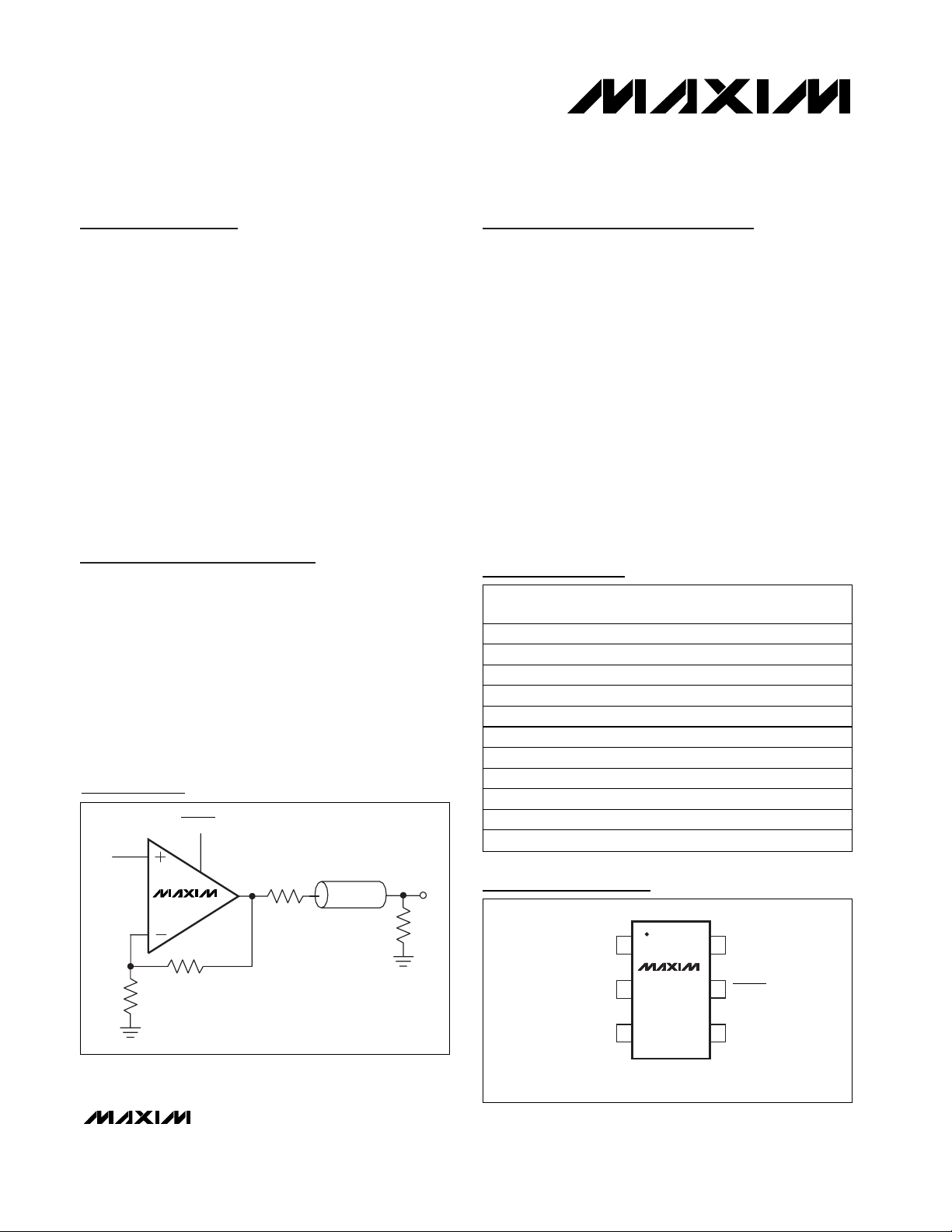
Video Line Driver
Features
♦ Low Cost and High Speed:
210MHz -3dB Bandwidth
55MHz 0.1dB Gain Flatness
485V/µs Slew Rate
♦ Disable Mode Places Outputs in High-Impedance
State
♦ Single +4.5V to +11V Operation
♦ Rail-to-Rail Outputs
♦ Input Common-Mode Range Extends Beyond V
EE
♦ Low Differential Gain/Phase: 0.02%/0.08°
♦ Low Distortion at 5MHz
-65dBc SFDR
-63dB Total Harmonic Distortion
♦ Ultra-Small 6-Pin SC70, 6-Pin SOT23, 10-Pin µMAX,
14-Pin TSSOP, and 20-Pin TSSOP Packages
MAX4380–MAX4384
Ultra-Small, Low-Cost, 210MHz, Single-Supply
Op Amps with Rail-to-Rail Outputs and Disable
500Ω
500Ω
75Ω
75Ω
IN
OUT
VIDEO LINE DRIVER
Z
o
= 75Ω
DISABLE
MAX4380
Typical Operating Circuit
19-2012; Rev 2; 4/03
Ordering Information
________________________________________________________________ Maxim Integrated Products 1
Pin Configurations
Pin Configurations continued at end of data sheet.
PART
TEMP RANGE
PIN-
TOP
MARK
6 SC70-6 AAV
—
MAX4381EUB
10 µMAX —
MAX4382EUD
14 TSSOP —
MAX4382ESD
14 SO —
MAX4382EEE
16 QSOP —
MAX4383EUD
14 TSSOP —
MAX4383ESD
14 SO —
MAX4383ESE
16 SO —
MAX4383EEE
16 QSOP —
MAX4384EUP
20 TSSOP —
For pricing, delivery, and ordering information, please contact Maxim/Dallas Direct! at
1-888-629-4642, or visit Maxim’s website at www.maxim-ic.com.
Rail-to-Rail is a registered trademark of Nippon Motorola, Ltd.
PACKAGE
MAX4380EXT-T -40°C to +85°C
MAX4380EUT-T -40°C to +85°C 6 SOT23-6
-40°C to +85°C
-40°C to +85°C
-40°C to +85°C
-40°C to +85°C
-40°C to +85°C
-40°C to +85°C
-40°C to +85°C
-40°C to +85°C
-40°C to +85°C
TOP VIEW
OUT
V
EE
16V
MAX4380
2
34
SC70-6/SOT23-6
CC
5 DISABLE
IN-IN+
MAX4380–MAX4384
Ultra-Small, Low-Cost, 210MHz, Single-Supply
Op Amps with Rail-to-Rail Outputs and Disable
2 _______________________________________________________________________________________
ABSOLUTE MAXIMUM RATINGS
Supply Voltage (VCCto VEE)................................................+12V
IN_-, IN_+, OUT_, DISABLE_ ...........(V
EE
- 0.3V) to (VCC+ 0.3V)
Output Short-Circuit to V
CC
or VEE...........................................1s
Continuous Power Dissipation (T
A
= +70°C)
6-Pin SC70 (derate 3.1mW/°C above +70°C) .............245mW
6-Pin SOT23 (derate 7.1mW/°C above +70°C) ...........571mW
10-Pin µMAX (derate 5.6mW/°C above +70°C) ..........444mW
14-Pin TSSOP (derate 9.1mW/°C above +70°C).........727mW
14-Pin SO (derate 8.3mW/°C above +70°C) ...............667mW
16-Pin QSOP (derate 8.3mW/°C above +70°C) ..........667mW
16-Pin Narrow SO (derate 8.7mW/°C above +70°C) ..696mW
20-Pin TSSOP (derate 10.9mW/°C above +70°C).......879mW
Operating Temperature Range. ..........................-40°C to +85°C
Junction Temperature......................................................+150°C
Storage Temperature Range .............................-65°C to +150°C
Lead Temperature (soldering, 10s) .................................+300°C
Stresses beyond those listed under “Absolute Maximum Ratings” may cause permanent damage to the device. These are stress ratings only, and functional
operation of the device at these or at any other conditions beyond those indicated in the operational sections of the specifications is not implied. Exposure
to absolute maximum rating conditions for extended periods may affect device reliability.
DC ELECTRICAL CHARACTERISTICS–Single Supply
(VCC= +5V, VEE= 0, VCM= VCC/2, V
OUT
= VCC/2, RL= ∞ to VCC/2, DISABLE_ = VCC(MAX4380/MAX4381/MAX4382/MAX4384),
T
A
= T
MIN
to T
MAX
, unless otherwise noted. Typical values are at TA= +25°C.) (Note 1)
PARAMETER SYMBOL CONDITIONS MIN TYP MAX UNITS
Input Common-Mode Voltage
Range
Input Offset Voltage
Input Offset Voltage Matching MAX4381–MAX4384 1 mV
Input Offset Voltage Tempco
Input Bias Current
Input Offset Current
Input Resistance
TC
V
CM
V
OS
VOS
I
B
I
OS
R
IN
Guaranteed by CMRR
TA = +25°C
TA = -40°C to +85°C
Differential mode (-1V ≤ V
Common mode (-0.2V ≤ VCM ≤ +2.75V) 3 MΩ
V
- 0.2 V
EE
CC
- 2.25
0.2 12
20
8 µV/°C
6.5 20 µA
0.5 7 µA
IN
≤ +1V)
70 kΩ
V
mV
Common-Mode Rejection Ratio CMRR
Open-Loop Gain
Output Voltage Swing
Output Current
Output Short-Circuit Current I
Open-Loop Output Resistance
A
V
I
R
VOL
OUT
OUT
SC
OUT
Power-Supply Rejection Ratio PSRR
- 0.2V ≤ VCM ≤ V
EE
0.25V ≤ V
0.8V ≤ V
1V ≤ V
≤ 4.75V, RL = 2kΩ
OUT
≤ 4.5V, RL = 150Ω
OUT
≤ 4V, RL = 50Ω 58
OUT
RL = 2kΩ
RL = 150Ω
RL = 75Ω
RL = 75Ω to
ground
Sinking from RL = 75Ω to V
Sourcing into RL = 75Ω to V
Sinking or sourcing
V
= +4.5V to +5.5V
S
- 2.25V
CC
VCC - V
V
OL
VCC - V
V
OL
VCC - V
V
OL
VCC - V
V
OL
- V
- V
- V
- V
CC
EE
OH
EE
OH
EE
OH
EE
OH
EE
70 95 dB
50 61
48 63
0.05 0.2
0.05 0.15
0.3 0.5
0.25 0.8
0.5 0.8
0.5 1.75
1 1.7
0.025 0.125
40 55
25 50
±100
8 Ω
50 62 dB
V
dB
V
mA
mA
MAX4380–MAX4384
Ultra-Small, Low-Cost, 210MHz, Single-Supply
Op Amps with Rail-to-Rail Outputs and Disable
_______________________________________________________________________________________ 3
DC ELECTRICAL CHARACTERISTICS–Single Supply
(VCC= +5V, VEE= 0, VCM= VCC/2, V
OUT
= VCC/2, RL= ∞ to VCC/2, DISABLE_ = VCC(MAX4380/MAX4381/MAX4382/MAX4384),
T
A
= T
MIN
to T
MAX
, unless otherwise noted. Typical values are at TA= +25°C.) (Note 1)
)
DC ELECTRICAL CHARACTERISTICS–Dual Supply
(VCC= +5V, VEE= -5V, VCM= 0, V
OUT
= 0, RL= ∞ to 0, DISABLE_ = VCC(MAX4380/MAX4381/MAX4382/MAX4384),
T
A
= T
MIN
to T
MAX
, unless otherwise noted. Typical values are at TA= +25°C.) (Note 1)
PARAMETER SYMBOL CONDITIONS MIN TYP MAX UNITS
Operating Supply Voltage
Range
Disabled Output Resistance
DISABLE_ Logic-Low Threshold
DISABLE_ Logic-High Threshold
DISABLE_ Logic Input Low
Current
DISABLE_ Logic Input High
Current
Quiescent Supply Current (Per
Amplifier)
V
OUT(OFF
R
V
V
I
IL
I
IH
I
IL
IH
S
Guaranteed by PSRR (Note 2) 4.5 11 V
S
DISABLE_ = 0, 0 ≤ V
DISABLE_ = 0
DISABLE_ = V
DISABLE_ = V
CC
CC
DISABLE_ = 0
OUT
≤ 5V
27 35 kΩ
V
- 1.25
CC
25 60 µA
10 40 µA
5.5 9
0.45 0.6
V
C C
- 3
PARAMETER SYMBOL CONDITIONS MIN TYP MAX UNITS
Input Common-Mode Voltage
Range
Input Offset Voltage
Input Offset Voltage Matching MAX4381–MAX4384 1 mV
Input Offset Voltage Tempco
Input Bias Current
Input Offset Current
Input Resistance
TC
V
CM
V
OS
VOS
I
B
I
OS
R
Guaranteed by CMRR
TA = +25°C
TA = T
Differential mode (-1V ≤ V
IN
Common mode (-5V ≤ VCM ≤ 2.75V) 3 MΩ
MIN
to T
MAX
IN
≤ +1V)
V
EE
V
C C
316
8 µV/°C
8.5 25 µA
0.5 12 µA
70 kΩ
- 2.25
24
V
V
mA
V
mV
Common-Mode Rejection Ratio CMRR
Open-Loop Gain
Output Voltage Swing
A
V
VOL
OUT
V
≤ VCM ≤ V
EE
-4.5V ≤ V
-4.25V ≤ V
-4V ≤ V
OUT
RL = 2kΩ
RL = 150Ω
RL = 75Ω
- 2.25V
CC
≤ +4.5V, RL = 2kΩ
OUT
≤ +4.25V, RL = 150Ω
OUT
70 95 dB
50 62
48 65
≤ +4V, RL = 50Ω 60
VCC - V
OH
V
- V
OL
EE
VCC - V
OH
V
- V
OL
EE
VCC - V
OH
V
- V
OL
EE
0.175 0.375
0.075 0.225
0.575 0.85
0.4 0.775
1.3 2.3
1.3 2.45
dB
V
MAX4380–MAX4384
Ultra-Small, Low-Cost, 210MHz, Single-Supply
Op Amps with Rail-to-Rail Outputs and Disable
4 _______________________________________________________________________________________
AC ELECTRICAL CHARACTERISTICS–Single Supply
(VCC= +5V, VEE= 0, VCM= +1.5V, RL= 100Ω to VCC/2, DISABLE_ = VCC(MAX4380/MAX4381/MAX4382/MAX4384),
V
OUT
= VCC/2, A
VCL
= +1V/V, TA= +25°C, unless otherwise noted.)
DC ELECTRICAL CHARACTERISTICS–Dual Supply (continued)
(VCC= +5V, VEE= -5V, VCM= 0, V
OUT
= 0, RL= ∞ to 0, DISABLE_ = VCC(MAX4380/MAX4381/MAX4382/MAX4384),
T
A
= T
MIN
to T
MAX
, unless otherwise noted. Typical values are at TA= +25°C.) (Note 1)
)
PARAMETER SYMBOL CONDITIONS MIN TYP MAX UNITS
Output Current
Output Short-Circuit Current I
Open-Loop Output Resistance
Power-Supply Rejection Ratio PSRR V
Operating Supply Voltage
Range
Disabled Output Resistance
R
DISABLE_ Logic-Low Threshold
DISABLE_ Logic-High Threshold
DISABLE_ Logic Input Low
Current
I
OUT
SC
R
OUT
V
S
OUT(OFF
V
IL
V
IH
I
IL
Sinking from RL = 75Ω to V
Sourcing into RL = 75Ω to V
CC
EE
Sinking or sourcing
= ±4.5V to ±5.5V 48 62 dB
S
Guaranteed by PSRR (Note 2) ±2.25 ±5.5 V
DISABLE_ = 0, -5V ≤ V
OUT
≤ 5V
DISABLE_ = 0
50 75
50 75
±100
8 Ω
27 35 kΩ
V
CC
V
- 1.25
CC
25 µA
- 3
mA
mA
V
V
DISABLE_ Logic Input High
Current
Quiescent Supply Current (Per
Amplifier)
I
IH
I
S
DISABLE_ = V
DISABLE_ = V
DISABLE_ = 0
CC
CC
10 µA
7.5 10
0.45 0.8
mA
PARAMETER SYMBOL CONDITIONS MIN TYP MAX UNITS
Small-Signal -3dB Bandwidth BW
Large-Signal -3dB Bandwidth BW
Small-Signal 0.1dB Gain
Flatness
Large-Signal 0.1dB Gain
Flatness
Slew Rate SR V
Settling Time to 0.1% t
Rise/Fall Time tR , t
Spurious-Free Dynamic Range SFDR fC = 5MHz, V
Two-Tone, Third-Order
Intermodulation Distortion
V
OUT
V
OUT
V
OUT
V
OUT
OUT
V
OUT
V
F
OUT
f
= 5MHz,
C
V
OUT
f1 = 4.7MHz, f2 = 4.8MHz,
V
OUT
BW
BW
SS
LS
0.1dBSS
0.1dBLS
S
IP3
= 100mVp-p 210 MHz
= 2Vp-p 175 MHz
= 100mVp-p 55 MHz
= 2Vp-p 40 MHz
= 2V step 485 V/µs
= 2V step 16 ns
= 100mVp-p 4 ns
= 2Vp-p -65 dBc
OUT
2nd harmonic -65
= 2Vp-p
= 1Vp-p
3rd harmonic -68Harmonic Distortion HD
Total harmonic
-63
-66 dBc
dBc
MAX4380–MAX4384
Ultra-Small, Low-Cost, 210MHz, Single-Supply
Op Amps with Rail-to-Rail Outputs and Disable
_______________________________________________________________________________________ 5
AC ELECTRICAL CHARACTERISTICS–Single Supply (continued)
(VCC= +5V, VEE= 0, VCM= +1.5V, RL= 100Ω to VCC/2, DISABLE_ = VCC(MAX4380/MAX4381/MAX4382/MAX4384),
V
OUT
= VCC/2, A
VCL
= +1V/V, TA= +25°C, unless otherwise noted.)
Note 1: All devices are 100% production tested at TA= +25°C. Specifications over temperature limits are guaranteed by design.
Note 2: PSRR for single +5V supply tested with V
EE
= 0, VCC= +4.5V to +5.5V; PSRR for dual ±5V supply tested with VEE= -4.5V
to -5.5V, V
CC
= +4.5V to +5.5V.
4
-6
100k 10M 100M1M 1G
SMALL-SIGNAL GAIN vs. FREQUENCY
MAX4380-84 toc01
FREQUENCY (Hz)
GAIN (dB)
-5
-4
-3
-2
-1
0
1
2
3
V
OUT
= 100mVp-p
4
-6
100k 10M 100M1M 1G
LARGE-SIGNAL GAIN vs. FREQUENCY
MAX4380-84 toc02
FREQUENCY (Hz)
GAIN (dB)
-5
-4
-3
-2
-1
0
1
2
3
V
OUT
= 2Vp-p
0.4
-0.6
100k 10M 100M1M 1G
SMALL-SIGNAL GAIN FLATNESS
vs. FREQUENCY
MAX4380-84 toc03
FREQUENCY (Hz)
GAIN (dB)
-0.5
-0.4
-0.3
-0.2
-0.1
0
0.1
0.2
0.3
V
OUT
= 100mVp-p
Typical Operating Characteristics
(VCC= +5V, VEE= 0, VCM= +1.5V, A
VCL
= +1V/V, RL= 100Ω to VCC/2, TA = +25°C, unless otherwise noted.)
PARAMETER SYMBOL CONDITIONS MIN TYP MAX UNITS
Channel-to-Channel Isolation CH
Input 1dB Compression Point fC = 10MHz, A
Differential Phase Error DP NTSC, RL = 150Ω 0.08 degrees
Differential Gain Error DG NTSC, RL = 150Ω 0.02 %
Input Noise-Voltage Density e
Input Noise-Current Density I
Input Capacitance C
Output Impedance Z
Enable Time t
Disable Time t
Specified at DC -102 dB
f = 10kHz 10 nV/√Hz
f = 10kHz 2 pA/√Hz
f = 10MHz 1.5 Ω
VIN = 1V (MAX4380/MAX4381/
MAX4382/MAX4384)
VIN = 1V (MAX4380/MAX4381/
MAX4382/MAX4384)
ISO
n
n
IN
OUT
ON
OFF
= +2V/V 14 dBm
VCL
1pF
100 ns
1µs

MAX4380–MAX4384
Ultra-Small, Low-Cost, 210MHz, Single-Supply
Op Amps with Rail-to-Rail Outputs and Disable
6 _______________________________________________________________________________________
Typical Operating Characteristics (continued)
(VCC= +5V, VEE= 0, VCM= +1.5V, A
VCL
= +1, RL= 100Ω to VCC/2, TA = +25°C, unless otherwise noted.)
-10
-100
100k 100M10M1M
DISTORTION vs. FREQUENCY
-70
-90
-30
-50
0
-60
-80
-20
-40
MAX4380-84 toc07
FREQUENCY (Hz)
DISTORTION (dBc)
2ND HARMONIC
3RD HARMONIC
V
OUT
= 2Vp-p
A
VCL
= +2V/V
-10
-100
100k 100M10M1M
DISTORTION vs. FREQUENCY
-70
-90
-30
-50
0
-60
-80
-20
-40
MAX4380-84 toc08
FREQUENCY (Hz)
DISTORTION (dBc)
2ND HARMONIC
3RD HARMONIC
V
OUT
= 2Vp-p
A
VCL
= +5V/V
-100
-70
-80
-90
-60
-50
-40
-30
-20
-10
0
0400200 600 800 1000 1200
DISTORTION vs. RESISTIVE LOAD
MAX4380-84 toc09
R
LOAD
(Ω)
DISTORTION (dBc)
2ND HARMONIC
3RD HARMONIC
fO = 5MHz
V
OUT
= 2Vp-p
A
VCL
= +1V/V
-100
-70
-80
-90
-60
-50
-40
-30
-20
-10
0
0.5 1.0
1.5
2.0
DISTORTION vs. VOLTAGE SWING
MAX4380-84 toc10
VOLTAGE SWING (Vp-p)
DISTORTION (dBc)
fO = 5MHz
A
VCL
= +1V/V
3RD HARMONIC
2ND HARMONIC
0100
0100
DIFFERENTIAL GAIN AND PHASE
-0.010
0
0.005
0.015
0.025
IRE
DIFF PHASE (degrees)
DIFF GAIN (%)
MAX4380-84 toc11
IRE
-0.005
0.020
0.010
-0.04
0.02
0.04
0.08
0.12
0
0.10
0.06
-0.02
0
-100
100k 10M 100M1M 1G
COMMON-MODE REJECTION
vs. FREQUENCY
MAX4380-84 toc12
FREQUENCY (Hz)
CMR (dB)
-90
-80
-70
-60
-50
-40
-30
-20
-10
0.3
-0.7
100k 1M 10M 100M 1G
LARGE-SIGNAL
GAIN FLATNESS vs. FREQUENCY
-0.5
MAX4380-84 toc04
FREQUENCY (Hz)
GAIN (dB)
-0.3
-0.1
0.1
0
-0.2
-0.4
-0.6
0.2
V
OUT
= 2V
P-P
100k 10M1M 100M 1G
OUTPUT IMPEDANCE vs. FREQUENCY
MAX4380-84 toc05
FREQUENCY (Hz)
IMPEDANCE (Ω)
100
0.01
0.1
1
10
2ND HARMONIC
3RD HARMONIC
-10
-100
100k 100M10M1M
DISTORTION vs. FREQUENCY
-70
-90
-30
-50
0
-60
-80
-20
-40
MAX4380-84 toc06
FREQUENCY (Hz)
DISTORTION (dBc)
V
OUT
= 2Vp-p
A
VCL
= +1V/V

MAX4380–MAX4384
Ultra-Small, Low-Cost, 200MHz, Single-Supply
Op Amps with Rail-to-Rail Outputs and Disable
_______________________________________________________________________________________ 7
Typical Operating Characteristics (continued)
(VCC= +5V, VEE= 0, VCM= +1.5V, A
VCL
= +1, RL= 100Ω to VCC/2, TA = +25°C, unless otherwise noted.)
MAX4380-84 toc15
INPUT
50mV/div
OUTPUT
50mV/div
SMALL-SIGNAL PULSE RESPONSE
20ns/div
A
VCL
= +1V/V
INPUT
25mV/div
OUTPUT
50mV/div
SMALL-SIGNAL PULSE RESPONSE
MAX4380-84 toc16
20ns/div
RF = 500Ω
A
VCL
= +2V/V
INPUT
10mV/div
OUTPUT
50mV/div
SMALL-SIGNAL PULSE RESPONSE
MAX4380-84 toc17
20ns/div
RF = 500Ω
A
VCL
= +5V/V
INPUT
1V/div
OUTPUT
1V/div
LARGE-SIGNAL PULSE RESPONSE
MAX4380-84 toc18
20ns/div
A
VCL
= +1V/V
INPUT
500mV/div
OUTPUT
1V/div
LARGE-SIGNAL PULSE RESPONSE
MAX4380-84 toc19
20ns/div
RF = 500Ω
A
VCL
= +2V/V
20ns/div
INPUT
200mV/div
OUTPUT
1V/div
LARGE-SIGNAL PULSE RESPONSE
MAX4380-84 toc20
RF = 500Ω
A
VCL
= +5V/V
0
-10
-20
-30
-40
-50
-60
-70
-80
100k 10M 100M1M 1G
POWER-SUPPLY REJECTION
vs. FREQUENCY
MAX4380-84 toc13
FREQUENCY (Hz)
PSR (dB)
0
0.2
0.1
0.3
0.6
0.7
0.5
0.4
0.8
0 100 150 200 25050 300 350 400 450 500
OUTPUT VOLTAGE SWING
vs. RESISTIVE LOAD
MAX4380-84 toc14a
R
LOAD
(Ω)
OUTPUT VOLTAGE SWING (V)
V
CC
- V
OH
V
OL
- V
EE
V
SUPPLY
= +5V
0
0.4
0.2
0.6
1.2
1.4
1.0
0.8
1.6
0 100 150 200 25050 300 350 400 450 500
OUTPUT VOLTAGE SWING
vs. RESISTIVE LOAD
MAX4380-84 toc14b
R
LOAD
(Ω)
OUTPUT VOLTAGE SWING (V)
V
CC
- V
OH
V
OL
- V
EE
V
SUPPLY
= ±5V

MAX4380–MAX4384
Ultra-Small, Low-Cost, 210MHz, Single-Supply
Op Amps with Rail-to-Rail Outputs and Disable
Typical Operating Characteristics (continued)
(VCC= +5V, VEE= 0, VCM= +1.5V, A
VCL
= +1, RL= 100Ω to VCC/2, TA = +25°C, unless otherwise noted.)
0
50
100
150
200
250
300
0 200100 300 400 500 600 700 800
SMALL-SIGNAL BANDWIDTH
vs. LOAD RESISTANCE
MAX4380-84 toc24
R
LOAD
(Ω)
BANDWIDTH (MHz)
80
0
100 1k 10k
OPEN-LOOP GAIN vs. RESISTIVE LOAD
20
10
MAX4380-84 toc25
R
LOAD
(Ω)
OPEN-LOOP GAIN (dB)
40
30
50
60
70
V
SUPPLY
= +5V
V
SUPPLY
= ±5V
CROSSTALK vs. FREQUENCY
MAX4380-84 toc26
FREQUENCY (Hz)
CROSSTALK (dB)
-140
-80
-100
-120
-60
-40
-20
0
20
40
60
0.1M 1M 10M 100M 1G
1
10k
10010 1k 100k
1M
10M
VOLTAGE NOISE vs. FREQUENCY
MAX4380-84 toc21
FREQUENCY (Hz)
1
10
100
RL = 100Ω
VOLTAGE NOISE (nV/√Hz)
CURRENT NOISE (pA/
√Hz)
1
10k
10010 1k 100k
1M
10M
CURRENT NOISE vs. FREQUENCY
MAX4380-84 toc22
FREQUENCY (Hz)
1
10
100
RL = 100Ω
9
11
10
13
12
15
14
16
0 200100 300 40050 250150 350 450 500
ISOLATION RESISTANCE
vs. CAPACITIVE LOAD
MAX4380-84 toc23
C
LOAD
(pF)
R
ISO
(
Ω
)
8 _______________________________________________________________________________________
SHUTDOWN RESPONSE
200ns/div
5V
1.5V
V
OUT
MAX4380-84 toc27
DISABLE
0
0
-5
-2
-3
-4
-1
0
1
2
3
4
5
-50 0-25 25 50 75 100
INPUT OFFSET VOLTAGE
vs. TEMPERATURE
MAX4380-84 toc28
TEMPERATURE (°C)
INPUT OFFSET VOLTAGE (mV)
V
SUPPLY
= ±5V
V
SUPPLY
= +5V
0
4
2
8
6
10
12
-50 0 25-25 50 75 100
INPUT BIAS CURRENT
vs. TEMPERATURE
A4380-84toc29
TEMPERATURE (°C)
INPUT BIAS CURRENT (mA)
V
SUPPLY
= +5V
V
SUPPLY
= ±5V

MAX4380–MAX4384
Ultra-Small, Low-Cost, 210MHz, Single-Supply
Op Amps with Rail-to-Rail Outputs and Disable
_______________________________________________________________________________________ 9
Pin Description
p
Typical Operating Characteristics (continued)
(VCC= +5V, VEE= 0, VCM= +1.5V, A
VCL
= +1, RL= 100Ω to VCC/2, TA = +25°C, unless otherwise noted.)
MAX4380 MAX4381 MAX4382 MAX4383 MAX4384
SC70/SOT23 µMAX QSOP SO/TSSOP SO/TSSOP SO/QSOP TSSOP
61044445V
SUPPLY CURRENT
10
9
8
7
6
5
4
3
SUPPLY CURRENT (mA)
2
1
0
-50 0-25 255075100
vs. TEMPERATURE
V
= ±5V
SUPPLY
V
= +5V
SUPPLY
TEMPERATURE (°C)
MAX4380-84 toc30
PIN
NAME FUNCTION
P osi ti ve P ow er S up pl y.
CC
C onnect a 0.1µF
capaci tor to GND .
N egati ve P ow er S up pl y.
2 4 13 11 11 13 16 V
EE
C onnect a 0.1µF
C apaci tor to GND .
3 —— — — — — IN+ N oni nver ti ng Inp ut
4 —— — — — — IN- Inver ting Inp ut
1 —— — — — — OUT Am pl i fier Outp ut
5 —— — — — —DISABLE
— 3 5 5 3 3 4 INA+
— 2 6 6 2 2 3 INA-
D i sab l e. C onnect to V
to E nabl e.
Am pl i fier A N oni nver ti ng
Input
Am pl i fier A Inver ting
Input
— 1 7 7 1 1 2 OUTA Am pl i fier A O utp ut
S hutd own Amp l i fi er A.
— 51 1 —— 1 DISABLEA
C onnect to V CC to
E nab l e.
— 7 12 10 5 5 6 INB+
Am pl i fier B N oni nver ti ng
ut
In
CC

MAX4380–MAX4384
Ultra-Small, Low-Cost, 210MHz, Single-Supply
Op Amps with Rail-to-Rail Outputs and Disable
10 ______________________________________________________________________________________10 ______________________________________________________________________________________
Detailed Description
The MAX4380–MAX4384 are single-supply, rail-to-rail,
voltage-feedback amplifiers that employ current-feedback techniques to achieve 485V/µs slew rates and
210MHz bandwidths. Excellent harmonic distortion and
differential gain/phase performance make these amplifiers an ideal choice for a wide variety of video and RF
signal-processing applications.
Applications Information
The output voltage swings to within 50mV of each supply rail. Local feedback around the output stage
ensures low open-loop output impedance to reduce
gain sensitivity to load variations. The input stage permits common-mode voltages beyond the negative supply and to within 2.25V of the positive supply rail.
Choosing Resistor Values
Unity-Gain Configuration
The MAX4380–MAX4384 are internally compensated
for unity gain. When configured for unity gain, a 24Ω
resistor (RF) in series with the feedback path optimizes
AC performance. This resistor improves AC response
by reducing the Q of the parallel LC circuit formed by
the parasitic feedback capacitance and inductance.
Video Line Driver
The MAX4380–MAX4384 are low-power, voltage-feedback amplifiers featuring bandwidths up to 210MHz,
0.1dB gain flatness to 55MHz. They are designed to
minimize differential-gain error and differential-phase
error to 0.02% and 0.08 degrees respectively. They
Pin Description (continued)
PIN
MAX4380 MAX4381 MAX4382 MAX4383 MAX4384
SC70/SOT23 µMAX QSOP SO/TSSOP SO/TSSOP SO/QSOP TSSOP
— 8 11 9 6 6 7 INB-
— 9 10 8 7 7 8 OUTB Amplifier B Output
— 63 3 —— 9 DISABLEB
——14 12 10 12 15 INC+
——15 13 9 11 14 INC-
——16 14 8 10 13 OUTC Amplifier C Output
——22 —— 12 DISABLEC
————12 14 17 IND+
————13 15 18 IND-
————14 16 19 OUTD Amplifier D Output
— ——— ——20 DISABLED
NAME FUNCTION
Am pl i fier B
Inver ting Inp ut
Shutdown Amplifier B.
C onnect to V
E nab l e.
Amplifier C
Noninverting Input
Amplifier C
Inverting Input
Shutdown Amplifier C.
C onnect to V
E nab l e.
Amplifier D
Noninverting Input
Amplifier D Inverting
Input
Shutdown Amplifier D.
C onnect to V CC to
E nab l e.
CC
CC
to
to
——8, 9 ——8, 9 10, 11 N.C.
No Connection. Not
internally connected.

MAX4380–MAX4384
Ultra-Small, Low-Cost, 210MHz, Single-Supply
Op Amps with Rail-to-Rail Outputs and Disable
______________________________________________________________________________________ 11
have a 16ns settling time to 0.1%, 485V/µs slew rates,
and output-current-drive capability of up to 75mA
making them ideal for driving video loads.
Inverting and Noninverting Configurations
Select the gain-setting feedback (R
F
) and input (RG)
resistor values to fit your application. Large resistor values increase voltage noise and interact with the amplifier’s input and PC board capacitance. This can
generate undesirable poles and zeros and decrease
bandwidth or cause oscillations. For example, a noninverting gain-of-two configuration (RF= RG) using 1kΩ
resistors, combined with 1pF of amplifier input capacitance and 1pF of PC board capacitance, causes a
pole at 159MHz. Since this pole is within the amplifier
bandwidth, it jeopardizes stability. Reducing the 1kΩ
resistors to 100Ω extends the pole frequency to
1.59GHz, but could limit output swing by adding 200Ω
in parallel with the amplifier’s load resistor
(Figures 1a and 1b).
Layout and Power-Supply Bypassing
These amplifiers operate from a single +4.5V to +11V
power supply or from dual ±2.25V to ±5.5V supplies. For
single-supply operation, bypass VCCto ground with a
0.1µF capacitor as close to the pin as possible. If operating with dual supplies, bypass each supply with a 0.1µF
capacitor.
Maxim recommends using microstrip and stripline
techniques to obtain full bandwidth. To ensure that the
PC board does not degrade the amplifier’s performance, design it for a frequency greater than 1GHz.
Pay careful attention to inputs and outputs to avoid
large parasitic capacitance. Whether or not you use a
constant-impedance board, observe the following
design guidelines:
• Don’t use wire-wrap boards; they are too inductive.
• Don’t use IC sockets; they increase parasitic capaci-
tance and inductance.
• Use surface-mount instead of through-hole components for better high-frequency performance.
• Use a PC board with at least two layers; it should be
as free from voids as possible.
• Keep signal lines as short and as straight as possible. Do not make 90° turns; round all corners.
Rail-to-Rail Outputs,
Ground-Sensing Inputs
For +5V single-supply operation, the input commonmode range extends from (VEE- 200mV) to (V
CC
- 2.25V) with excellent common-mode rejection.
Beyond this range, the amplifier output is a nonlinear
function of the input, but does not undergo phase
reversal or latchup.
For ±5V dual-supply operation, the common-mode
range is from VEEto (VCC- 2.25V)
For +5V single-supply operation the output swings to
within 50mV of either power-supply rail with a 2kΩ
load. The input ground sensing and the rail-to-rail output substantially increase the dynamic range. With a
symmetric input in a single +5V application, the input
can swing 2.95Vp-p and the output can swing 4.9Vp-p
with minimal distortion.
Low-Power Disable Mode
The disable feature (DISABLE_) allows the amplifier to
be placed in a low-power, high-output-impedance
state. When the disable pin (DISABLE_) is active, the
amplifier’s output impedance is 35kΩ. This high resistance and the low 2pF output capacitance make the
MAX4380–MAX4382 and the MAX4384 ideal in
RF/video multiplexer or switch applications. For larger
arrays, pay careful attention to capacitive loading.
Refer to the Output Capacitive Loading and Stability
section.
Figure 1b. Inverting Gain Configuration
Figure 1a. Noninverting Gain Configuration
MAX438 _
MAX438 _
V
R
F
V
OUT
R
F
= -(RF / RG) V
OUT
V
OUT
= [1+ (RF / RG)] V
V
OUT
IN
IN
R
G
IN
R
IN
G

MAX4380–MAX4384
Ultra-Small, Low-Cost, 210MHz, Single-Supply
Op Amps with Rail-to-Rail Outputs and Disable
12 ______________________________________________________________________________________
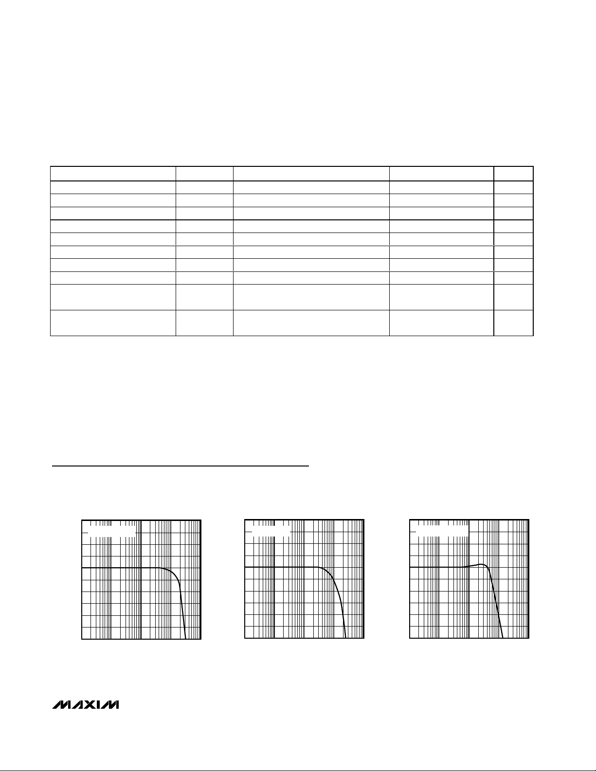
Output Capacitive Loading and Stability
The MAX4380–MAX4384 are optimized for AC performance. They are not designed to drive highly reactive
loads, which decrease phase margin and may produce
excessive ringing and oscillation. Figure 2 shows a circuit that eliminates this problem. Figure 3 is a graph of
the Optimal Isolation Resistor (RS) vs. Capacitive Load.
Figure 4 shows how a capacitive load causes excessive peaking of the amplifier’s frequency response if
the capacitor is not isolated from the amplifier by a
resistor. A small isolation resistor (usually 10Ω to 15Ω)
placed before the reactive load prevents ringing and
oscillation. At higher capacitive loads, AC performance
is controlled by the interaction of the load capacitance
and the isolation resistor. Figure 5 shows the effect of a
15Ω isolation resistor on closed-loop response.
Chip Information
MAX4380 TRANSISTOR COUNT: 66
MAX4381 TRANSISTOR COUNT: 132
MAX4382 TRANSISTOR COUNT: 196
MAX4383 TRANSISTOR COUNT: 264
MAX4384 TRANSISTOR COUNT: 264
Figure 4. Small-Signal Gain vs. Frequency with Load
Capacitance and No Isolation Resistor
Figure 5. Small-Signal Gain vs. Frequency with Load
Capacitance and 27Ω Isolation Resistor
Figure 2. Driving a Capacitive Load Through an Isolation Resistor
Figure 3. Isolation Resistance vs. Capacitive Load
MAX438 _
R
F
R
ISO
V
OUT
C
L
R
G
V
IN
ISOLATION RESISTANCE
vs. CAPACITIVE LOAD
16
15
14
13
(Ω)
ISO
R
12
11
10
9
0 200100 300 40050 250150 350 450 500
C
(pF)
LOAD
MAX4380-84 toc23
6
5
4
3
2
1
GAIN (dB)
0
-1
-2
-3
-4
100k 10M 100M1M 1G
CL = 10pF
CL = 5pF
FREQUENCY (Hz)
CL = 15pF
3
R
= 15Ω
ISO
2
1
0
-1
-2
GAIN (dB)
-3
-4
-5
-6
-7
100k 10M 100M1M 1G
CL = 68pF
CL = 120pF
FREQUENCY (Hz)
CL = 47pF

MAX4380–MAX4384
Ultra-Small, Low-Cost, 210MHz, Single-Supply
Op Amps with Rail-to-Rail Outputs and Disable
______________________________________________________________________________________ 13
Pin Configurations (continued)
TOP VIEW
TOP VIEW
OUTA
INA-
INA+
DISABLEA
DISABLEC
DISABLEB
V
INA+
INA-
TOP VIEW
16
15
INC-
14
INC+
13
V
EE
12
INB+
INB-
11
10
OUTB
9
N.C.
14
OUTD
13
IND-
12
IND+
11
V
EE
INC+
10
9
INC-
OUTCOUTB
8
V
INA+
INA-
OUTA
N.C.
1
2
3
MAX4382
4
CC
5
6
7
8
DISABLEA OUTC
1
2
MAX4381
3
4
EE
5
10
V
CC
OUTB
9
INB-
8
INB+V
7
DISABLEBDISABLEA
6
DISABLEC
DISABLEB
µMAX-10
QSOP
TOP VIEW
1
2
3
4
CC
MAX4382
5
6
7
14
OUTC
13
INC-
12
INC+
11
V
EE
INB+
10
9
INB-
OUTBOUTA
8
OUTA
INA-
INA+
V
INB+
INB-
1
2
3
4
CC
MAX4383
5
6
7
TOP VIEW
TSSOP/SO
SO/TSSOP
TOP VIEW
1
OUTA OUTD
INA-
2
INA+
3
MAX4383
4
V
CC
INB+
5
INB-
6
OUTB
7
N.C.
8
SO/QSOP
16
15
IND-
14
IND+
13
V
EE
INC+
12
INC-
11
OUTC
10
N.C.
9
DISABLEA
OUTA
INA-
V
INB+
INB-
DISABLEB
1
2
3
4
MAX4384
5
CC
6
7
8
9
10
20
19
18
17
16
15
14
13
12
11
DISABLED
OUTD
IND-
IND+INA+
V
EE
INC+
INC-
OUTCOUTB
DISABLEC
N.C.N.C.
TSSOP

MAX4380–MAX4384
Ultra-Small, Low-Cost, 210MHz, Single-Supply
Op Amps with Rail-to-Rail Outputs and Disable
14 ______________________________________________________________________________________
Package Information
(The package drawing(s) in this data sheet may not reflect the most current specifications. For the latest package outline information
go to www.maxim-ic.com/packages
.)
SC70, 6L.EPS
PACKAGE OUTLINE, SOT-23, 6L
21-0058
1
F
1
6LSOT.EPS

MAX4380–MAX4384
Ultra-Small, Low-Cost, 210MHz, Single-Supply
Op Amps with Rail-to-Rail Outputs and Disable
______________________________________________________________________________________ 15
Package Information (continued)
(The package drawing(s) in this data sheet may not reflect the most current specifications. For the latest package outline information
go to www.maxim-ic.com/packages
.)
0.6±0.1
e
10
ÿ 0.50±0.1
1
0.6±0.1
TOP VIEW
D2
A2
D1
FRONT VIEW
4X S
H
BOTTOM VIEW
GAGE PLANE
A
b
α
A1
10
1
E2
E1
L
L1
INCHES
MILLIMETERS
MAX
DIM
MIN
-A
0.002
A1
A2 0.030 0.037 0.75 0.95
0.116
D1
0.114
D2
0.116
E1
0.114
E2
0.187
H
0.0157
L
L1
0.037 REF
0.007
b
e
0.0197 BSC
0.0035
c
0.0196 REF
S
α
0∞ 0∞ 6∞
c
0.043
0.006
0.120
0.118
0.120
0.118
0.199
0.0275
0.0106
0.0078
MIN
-
0.05
2.95
2.89
2.95
2.89
4.75
0.40
0.940 REF
0.177
0.500 BSC
0.090
0.498 REF
6∞
MAX
1.10
0.15
3.05
3.00
3.05
3.00
5.05
0.70
0.270
0.200
10LUMAX.EPS
SIDE VIEW
PROPRIETARY INFORMATION
TITLE:
PACKAGE OUTLINE, 10L uMAX/uSOP
21-0061
REV.DOCUMENT CONTROL NO.APPROVAL
1
I
1
INCHES
DIM
MIN
N
HE
1
TOP VIEW
0.053A
0.004
A1
0.014
B
0.007
C
e 0.050 BSC 1.27 BSC
0.150
E
H 0.2440.228 5.80 6.20
0.016L
VARIATIONS:
INCHES
MINDIM
D
0.189 0.197 AA5.004.80 8
0.337 0.344 AB8.758.55 14
D
MAX
0.069
0.010
0.019
0.010
0.157
0.050
MAX
0.3940.386D
MILLIMETERS
MAX
MIN
1.35
1.75
0.10
0.25
0.35
0.49
0.19
0.25
3.80 4.00
0.40 1.27
MILLIMETERS
MAX
MIN
9.80 10.00
N MS012
16
AC
SOICN .EPS
D
C
L
0∞-8∞
SIDE VIEW
PROPRIETARY INFORMATION
TITLE:
PACKAGE OUTLINE, .150" SOIC
21-0041
REV.DOCUMENT CONTROL NO.APPROVAL
1
B
1
e
FRONT VIEW
A
B
A1

Maxim cannot assume responsibility for use of any circuitry other than circuitry entirely embodied in a Maxim product. No circuit patent licenses are
implied. Maxim reserves the right to change the circuitry and specifications without notice at any time.
16 Maxim Integrated Products, 120 San Gabriel Drive, Sunnyvale, CA 94086 408-1737-7600
© 2003 Maxim Integrated Products Printed USA is a registered trademark of Maxim Integrated Products.
MAX4380–MAX4384
Ultra-Small, Low-Cost, 210MHz, Single-Supply
Op Amps with Rail-to-Rail Outputs and Disable
QSOP.EPS
Package Information (continued)
(The package drawing(s) in this data sheet may not reflect the most current specifications. For the latest package outline information
go to www.maxim-ic.com/packages
.)
TSSOP4.40mm.EPS
 Loading...