Maxim MAX4370ESA Datasheet

For free samples & the latest literature: http://www.maxim-ic.com, or phone 1-800-998-8800.
For small orders, phone 1-800-835-8769.
General Description
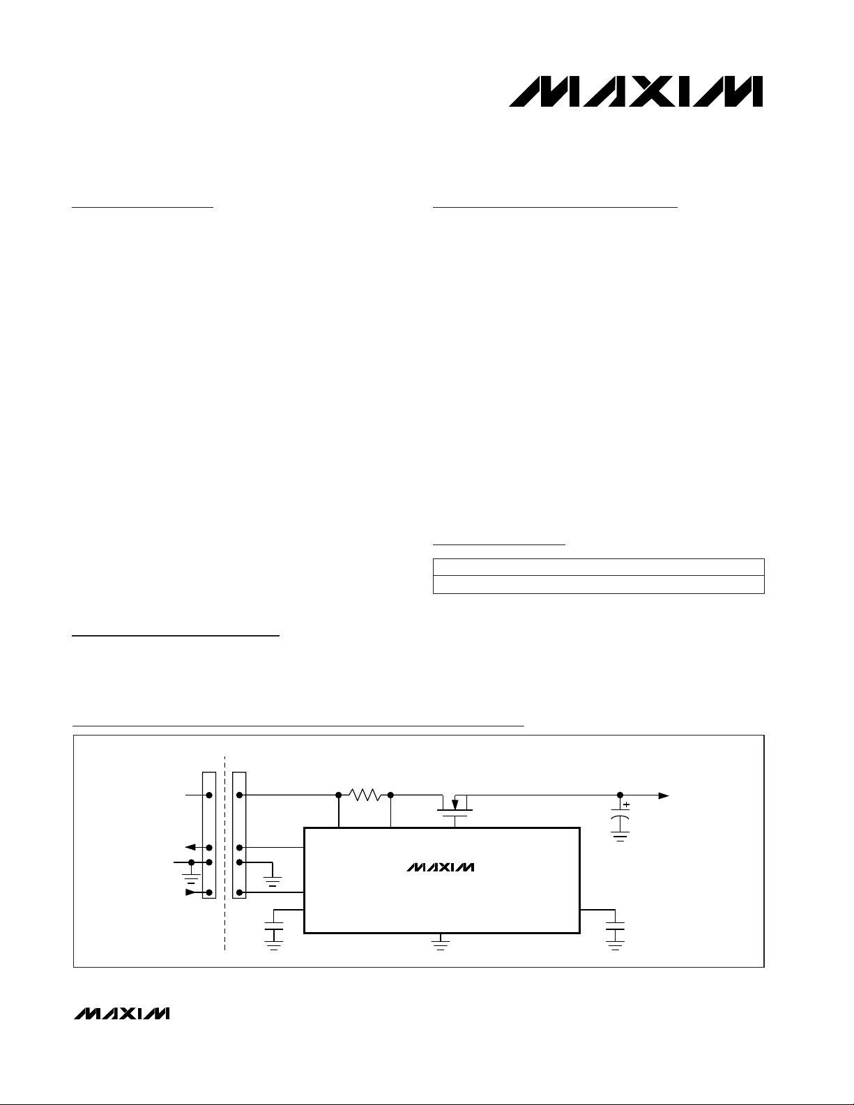
The MAX4370 is a circuit-breaker IC designed to offer
protection in hot-swap applications using Maxim’s
DualSpeed/BiLevel™ detection. This controller,
designed to reside either on the backplane or on the
removable card, is used to protect a system from startup damage when a card or board is inserted into a rack
with the main system power supply turned on. The
card’s discharged filter capacitors provide a low
impedance that can momentarily cause the main power
supply to collapse. The MAX4370 prevents this start-up
condition by providing inrush current regulation during
a programmable start-up period, allowing the system to
stabilize safely. In addition, two on-chip comparators
provide DualSpeed/BiLevel short-circuit protection and
overcurrent protection during normal operation.
The MAX4370 provides protection for a +3V to +12V
single supply. An internal charge pump generates the
controlled gate drive for an external N-channel MOSFET power switch. The MAX4370 latches the switch off
after a fault condition until an external reset signal
clears the device. Other features include a status pin to
indicate a fault condition, an adjustable overcurrent
response time, and a power-on reset comparator.
The MAX4370 is specified for the extended-industrial
temperature range (-40°C to +85°C) and is available in
an 8-pin SO package.
Applications
Hot Board Insertion
Solid-State Circuit Breaker
Features
♦ DualSpeed/BiLevel Protection During Normal
Operation
♦ Inrush Current Regulated at Start-Up
♦ Resides Either on the Backplane or on the
Removable Card
♦ Programmable Start-Up Period and Response
Time
♦ Allows Safe Board Insertion and Removal from
Live Backplane
♦ Protection for +3V to +12V Single Supplies
♦ Latched Off After Fault Condition
♦ Status Output Pin
♦ Internal Charge Pump Generates Gate Drive for
External N-Channel MOSFET
MAX4370
†
Current-Regulating Hot-Swap Controller with
DualSpeed/BiLevel Fault Protection
________________________________________________________________
Maxim Integrated Products
1
N
M1
MAX4370
V
OUT
C
BOARD
CTIM
C
TIM
CSPD
C
SPD
ON
ON
GND
STAT
V
CC
R
SENSE
STAT
REMOVABLE CARDBACKPLANE
V
IN
VSEN GATE
GND
Typical Operating Circuit
19-1472; Rev 0; 4/99
PART
MAX4370ESA -40°C to +85°C
TEMP. RANGE PIN-PACKAGE
8 SO
Ordering Information
DualSpeed/BiLevel is a trademark of Maxim Integrated Products.
†
Patent Pending
Pin Configuration appears at end of data sheet.

MAX4370
Current-Regulating Hot-Swap Controller with
DualSpeed/BiLevel Fault Protection
2 _______________________________________________________________________________________
ABSOLUTE MAXIMUM RATINGS
ELECTRICAL CHARACTERISTICS
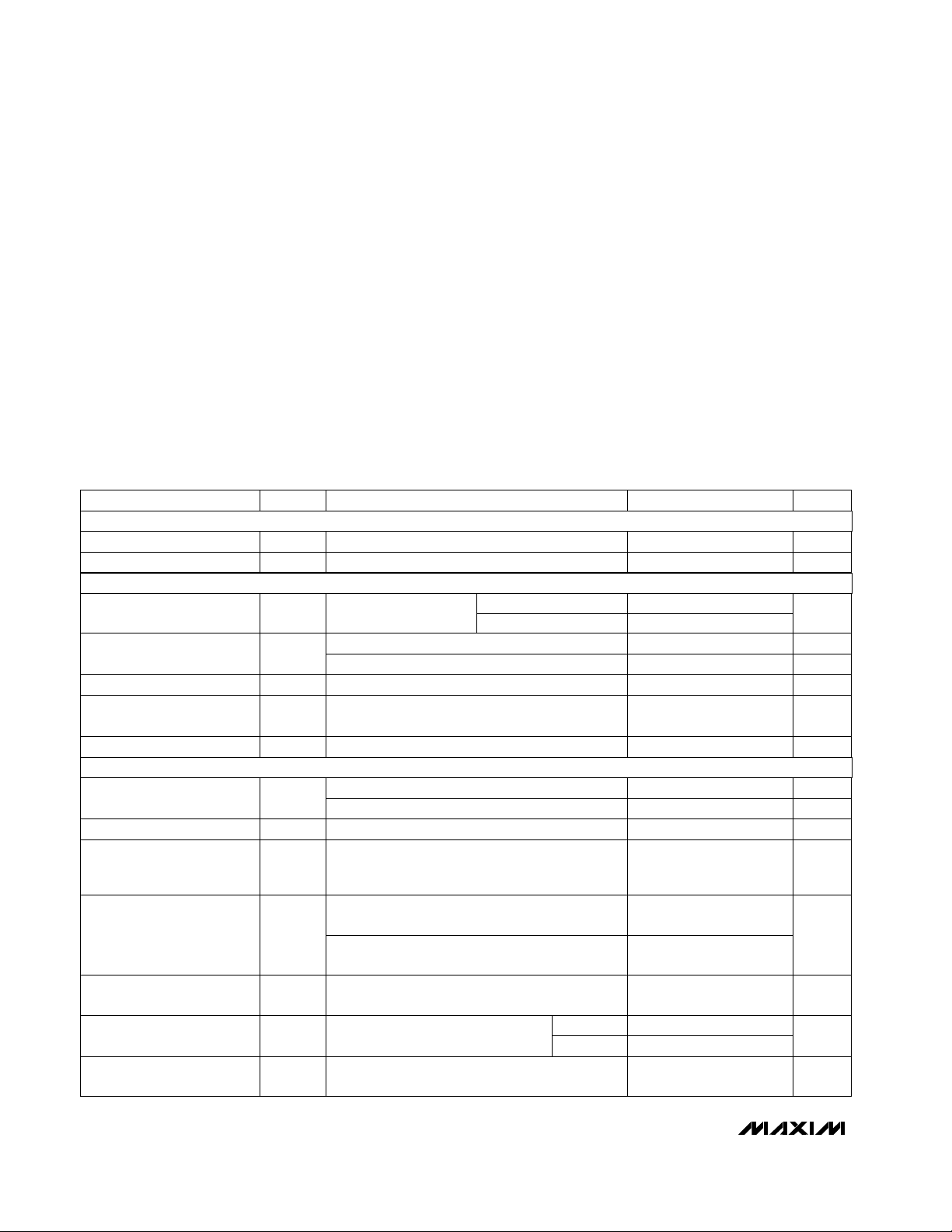
(VIN= +2.7V to +13.2V, TA= -40°C to +85°C, unless otherwise noted. Typical values are at VIN= +5V and TA= +25°C.) (Note 2)
Stresses beyond those listed under “Absolute Maximum Ratings” may cause permanent damage to the device. These are stress ratings only, and functional
operation of the device at these or any other conditions beyond those indicated in the operational sections of the specifications is not implied. Exposure to
absolute maximum rating conditions for extended periods may affect device reliability.
Note 1: ON can be pulled below ground. Limiting the current to 2mA ensures that this pin is never lower than about -0.8V.
V
IN
to GND...........................................................................+15V
STAT to GND..........................................................-0.3V to +14V
GATE to GND ..............................................-0.3V to (V
IN
+ 8.5V)
ON to GND (Note 1)................................................. -1V to +14V
CSPD to GND.............-0.3V to the lower of (V
IN
+ 0.3V) or +12V
VSEN, CTIM to GND....................................-0.3V to (V
IN
+ 0.3V)
Current into ON...................................................................±2mA
Current into Any Other Pin................................................±50mA
Continuous Power Dissipation (T
A
= +70°C)
SO (derate 5.9mW/°C above +70°C)........................... 471mW
Operating Temperature Range ...........................-40°C to +85°C
Storage Temperature Range.............................-65°C to +150°C
Lead Temperature (soldering, 10sec)............................ +300°C
Start-up is initiated only if V
GATE
is less than this
voltage
ON = V
IN
I
GATE
= 8.5µA, measured above V
IN
Measured with respect to VIN; voltage at which
internal clamp circuitry is triggered
During start-up (current regulation provided by
fast comparator)
Time from current overload to V
GATE
< 0.1V,
C
GATE
= 1000pF to GND (triggered by the fast
comparator during normal operation)
VSEN = V
IN
V
GATE
= VIN(Note 4)
CTIM = floating
10mV overdrive, from overload condition to GATE
discharging
VIN- VSEN
VIN- V
SEN
CSPD = floating
100nF on CTIM
100nF on CSPD to GND
CONDITIONS
V0.1Gate Overvoltage Threshold
V
2.7
5
Minimum Gate Drive Voltage
V6.7 7.5Maximum Gate Voltage
80
Gate Discharge Current
µs60t
OFF
Turn-Off Time
µA100I
GATE
Gate Charge Current
µs5.5
ms21 31 41
t
START
Start-Up Period
(Note 3)
mA0.6 1I
Q
Supply Current
V2.7 13.2V
IN
Input Voltage Range
µA0.2 10I
B,VSEN
VSEN Input Bias Current
ns460t
FCD
Fast Comparator Response
Time
mV180 200 220V
FC,TH
Fast Comparator Threshold
mV
45 50 55
V
SC,TH
Slow Comparator
Threshold
µs10 20 40
t
CSPD
Slow Comparator Response
Time
ms10 20 40
UNITSMIN TYP MAXSYMBOLPARAMETER
During turn-off, triggered by a fault in normal
operation or ON falling edge
µA
75 225 550
I
GATE,DIS
POWER SUPPLIES
MOSFET DRIVER
CURRENT CONTROL
VIN≥ 5V
VIN≥ 2.7V
TA= +25°C
TA= T
MIN
to T
MAX
43.5 56

MAX4370
Current-Regulating Hot-Swap Controller with
DualSpeed/BiLevel Fault Protection
_______________________________________________________________________________________ 3
ELECTRICAL CHARACTERISTICS (continued)
(VIN= +2.7V to +13.2V, TA= -40°C to +85°C, unless otherwise noted. Typical values are at VIN= +5V and TA= +25°C.) (Note 2)
Note 2: All devices are 100% tested at T
A
= +25°C. All temperature limits are guaranteed by design.
Note 3: The start-up period (t
START
) is the time during which the slow comparator is ignored and the device acts as a current limiter
by regulating the sense current with the fast comparator. It is measured from ON rising above 0.6V to STAT rising.
Note 4: The current available at GATE is a function of V
GATE
(see Typical
Operating Characteristics.
)
VIN= 5V, rising threshold
CONDITIONS
mV3V
HYST
Hysteresis
V0.575 0.6 0.625V
TH,ON
Threshold Voltage
UNITSMIN TYP MAXSYMBOLPARAMETER
2.7V ≤ VIN≤ 13.2V mV/V0.1 1PSRR
Power-Supply Rejection
Ratio
Input can be driven to the absolute maximum
limit without false output inversion
V-0.1 13.2
10mV overdrive
V
ON
Input Voltage Range
µs10t
D,COMP
Propagation Delay
µA0.001 1I
B,ON
Input Bias Current
To restart after a fault µs20t
RESTART
ON Pulse Width Low
V
STAT
≤ +13.2V µA1Output Leakage Current
I
SINK
= 1mA V0.4V
OL
Output Voltage Low
Start-up is initiated when this threshold is
reached at V
IN
V2.25 2.67V
UVLO
Threshold
mV100V
UVLO,HYST
Hysteresis
Time which input voltage must exceed undervoltage lockout before start-up is initiated
ms100 150 200t
D,UVLO
UVLO to Start-Up Delay
DIGITAL OUTPUT (STAT)
ON COMPARATOR
VINUNDERVOLTAGE LOCKOUT

MAX4370
Current-Regulating Hot-Swap Controller with
DualSpeed/BiLevel Fault Protection
4 _______________________________________________________________________________________
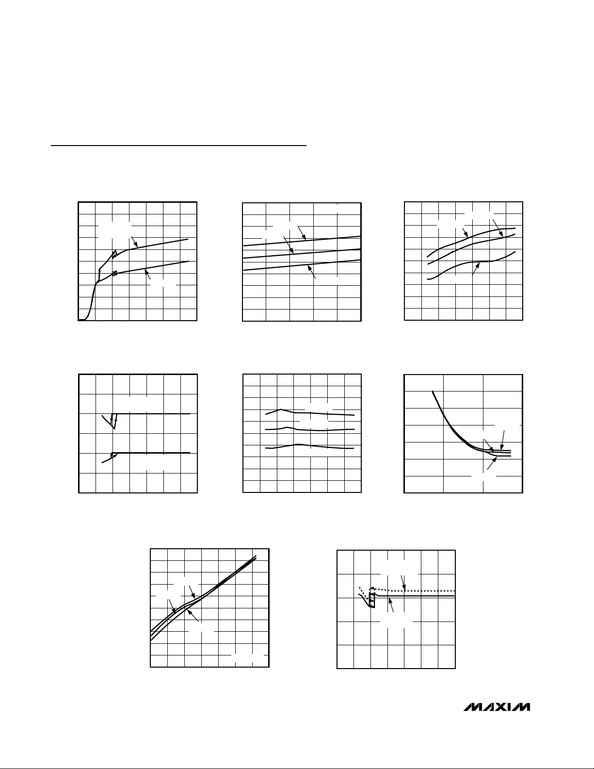
Typical Operating Characteristics
(Circuit of Figure 7, VIN= 5V, R
SENSE
= 100mΩ, M1 = FDS6670A, C
BOARD
= 470µF, C
GATE
= 0, RS= 0, TA= +25°C, unless other-
wise noted.)
0
0.3
0.2
0.1
0.5
0.4
0.9
0.8
0.7
0.6
1.0
02468101214
SUPPLY CURRENT vs. INPUT VOLTAGE
MAX4370 toc01
VIN (V)
SUPPLY CURRENT (mA)
ON = V
IN
I
GATE
= 10µA
ON = GND
-40 -15 10 35 60 85
SUPPLY CURRENT vs. TEMPERATURE
MAX4370 toc02
TEMPERATURE (°C)
0
0.3
0.2
0.1
0.5
0.4
0.9
0.8
0.7
0.6
1.0
SUPPLY CURRENT (mA)
ON = V
IN
VIN = 12V
VIN = 5V
VIN = 3V
49.0
49.6
49.4
49.2
50.0
49.8
50.8
50.6
50.4
50.2
51.0
02468101214
SLOW COMPARATOR THRESHOLD
vs. INPUT VOLTAGE
MAX4370 toc03
VIN (V)
V
SC, TH
(mV)
TA = -40°C
TA = +25°C
TA = +85°C
0
200
100
400
300
600
500
700
1 10 100 1000
FAST COMPARATOR RESPONSE TIME
vs. OVERDRIVE VOLTAGE
MAX4370 toc07
VOD (mV)
t
FCD
(ns)
VIN = 3V
VIN = 5V
VIN = 12V
18
20
19
22
21
23
24
18
20
19
22
21
23
24
0682 4 10 12 14
SLOW COMPARATOR
RESPONSE TIME vs. INPUT VOLTAGE
MAX4370 toc05
VIN (V)
t
CSPD
(µs)
t
CSPD
(ms)
CSPD = 110nF
TIME IN ms
CSPD = 0
TIME IN µs
190
196
194
192
200
198
108
206
204
202
210
FAST COMPARATOR THRESHOLD
vs. INPUT VOLTAGE
MAX4370 toc06
V
FC, TH
(mV)
02468101214
V
IN
(V)
TA = -40°C
TA = +25°C
TA = +85°C
400
430
420
410
450
440
490
480
470
460
500
-40 -20 0 20 40 60 80 100
FAST COMPARATOR RESPONSE TIME
vs. TEMPERATURE
MAX4370 toc08
TEMPERATURE (°C)
t
FCD
(ns)
VIN = 12V
VIN = 3V
VOD = 10mV
VIN = 5V
250
270
310
290
330
350
042 6 8101214
START-UP TIME
vs. INPUT VOLTAGE
MAX4370 toc09
VIN (V)
t
START
(µs)
25
27
31
29
33
35
t
START
(ms)
C
TIM
= 100nF
TIME IN ms
C
TIM
= 1nF
TIME IN µs

MAX4370
Current-Regulating Hot-Swap Controller with
DualSpeed/BiLevel Fault Protection
_______________________________________________________________________________________
5
0
60
40
20
80
100
120
0862 4 10 12 14 16 18 20
GATE CHARGE CURRENT
vs. GATE VOLTAGE
MAX4370 toc10
V
GATE
(V)
I
GATE
(µA)
VIN = 12V
VIN = 5.0V
VIN = 3.0V
0
50
25
100
75
125
150
-40 -10 35-15 60 85
GATE CHARGE CURRENT
vs. TEMPERATURE
MAX4370 toc11
TEMPERATURE (°C)
I
GATE
(µA)
VIN = 12V
V
GATE
= 0
VIN = 5V
VIN = 3V
0
5
15
10
20
25
042 6 8101214
GATE VOLTAGE vs. INPUT VOLTAGE
MAX4370 toc12
VIN (V)
V
GATE
(V)
I
GATE
= 10µA
TA = +85°C
TA = +25°C
TA = -40°C
0
100
50
150
300
350
250
200
400
0 468102 1214161820
GATE DISCHARGE CURRENT
vs. GATE VOLTAGE
MAX4370 toc13
V
GATE
(V)
I
GATE
(µA)
VIN = 12V
VIN = 3V
TRIGGERED BY A FAULT
OR BY ON FALLING
VIN = 5V
C
BOARD
= 0, R
SENSE
= 100mΩ,
C
TIM
= 10nF, C
GATE
= 0
V
OUT
(2V/div)
V
GATE
(2V/div)
ON
100µs/div
START-UP TIME (C
BOARD
= 0)
MAX4370-16
0
100
50
200
150
350
300
250
400
-40 10-15 35 60 85
GATE DISCHARGE CURRENT
vs. TEMPERATURE
MAX4370 toc14
TEMPERATURE (°C)
I
GATE
(µA)
VIN = 3V
VIN = 5V & 12V
V
GATE
= V
IN
TRIGGERED BY A FAULT
OR BY ON FALLING
C
BOARD
= 470µF, R
SENSE
= 100mΩ,
C
TIM
= 10nF, C
GATE
= 0
I
LOAD
(1A/div)
V
OUT
(2V/div)
V
GATE
(2V/div)
ON
500µs/div
START-UP TIME (C
BOARD
= 470µF)
MAX4370-15
C
BOARD
= 470µF, R
SENSE
= 100mΩ,
C
GATE
= 22nF, C
TIM
= 10nF, RS = 0
I
LOAD
(1A/div)
V
OUT
(2V/div)
V
GATE
(2V/div)
ON
1ms/div
START-UP TIME
(EXTERNAL C
GATE
= 22nF, C
BOARD
= 470µF)
MAX4370-17
C
BOARD
= 470µF, R
SENSE
= 100mΩ,
C
GATE
= 0
I
LOAD
(1A/div)
V
OUT
(2V/div)
V
GATE
(2V/div)
0A
50µs/div
TURN-OFF TIME (C
BOARD
= 470µF)
MAX4370-18
ON
0V
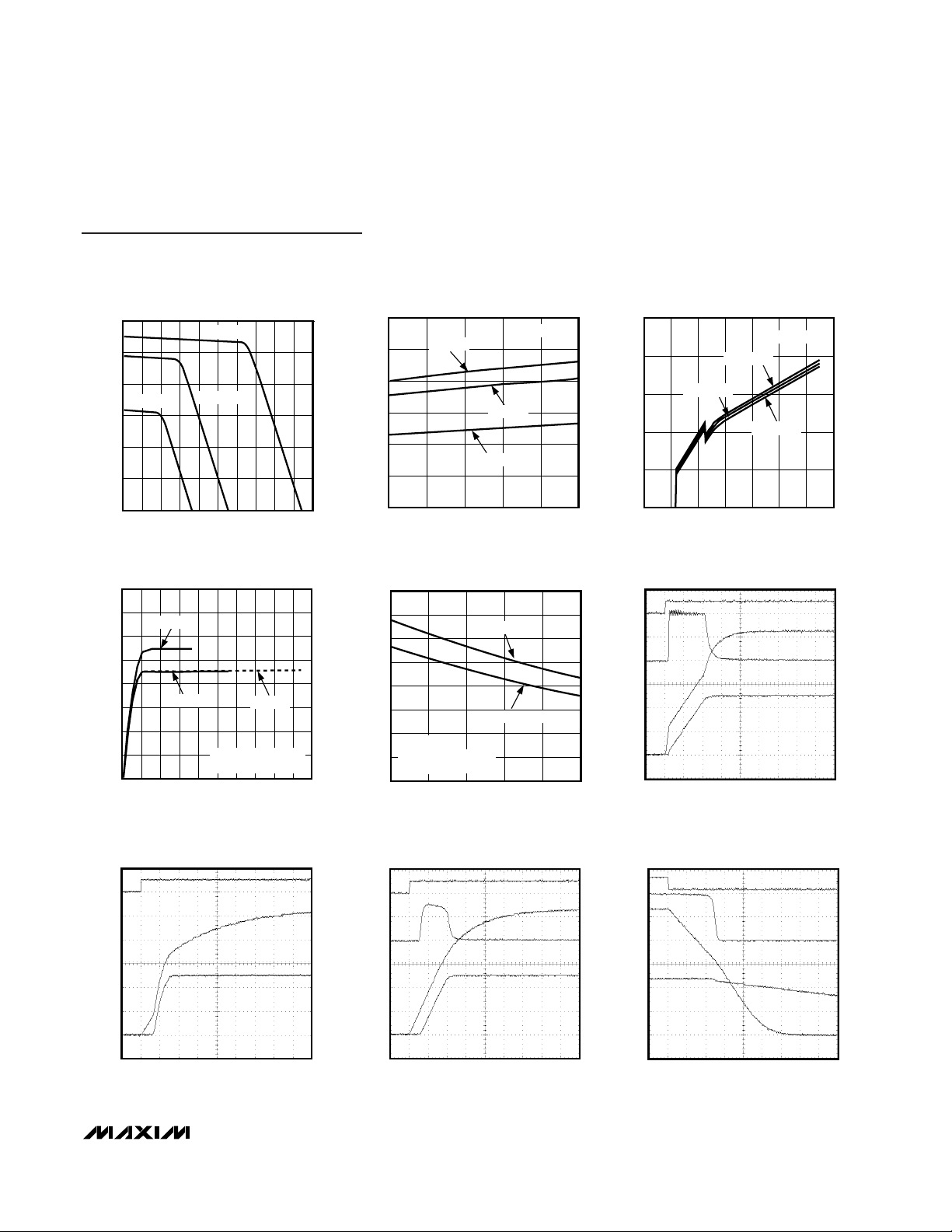
Typical Operating Characteristics (continued)
(Circuit of Figure 7, VIN= 5V, R
SENSE
= 100mΩ, M1 = FDS6670A, C
BOARD
= 470µF, C
GATE
= 0, RS= 0, TA= +25°C, unless other-
wise noted.)
 Loading...