

Page 1
General Description
The MAX4361/MAX4362/MAX4363 are a family of highperformance ADSL drivers and drivers/receivers ideal
for the upstream transmit path and the downstream
receive path of customer premise equipment. These
devices operate from a single 5V supply and deliver up
to 12.5dBm average line power for DMT modulated signals, meeting the requirements of full-rate ADSL.
Spurious-free dynamic range (SFDR) at full output
power is typically -75dBC at 100kHz.
The MAX4361 is a differential IN/differential OUT driver
with a fixed gain of 3.1V/V. The MAX4362 is a dual
amplifier with shutdown intended for use as a differential IN/differential OUT driver with gain set with external
resistors. The MAX4363 is a quad amplifier with shutdown intended for use as a differential IN/differential
OUT driver/receiver combination with gain set with
external resistors.
The MAX4361 is offered in a space-saving 8-pin µMAX
package.
Applications
ADSL Line Interface
HDSL Line Driver
Features
♦ Low-Noise Driver
4.8nV/√Hz Voltage-Noise Density
1.5pA/√Hz Current-Noise Density
♦ Full-Rate ADSL ATU-R Line Drivers and Receivers
♦ Single 5V Supply
♦ -75dBc SFDR at Full Output Power at 100kHz
♦ -95dB Driver-to-Receiver Crosstalk (MAX4363)
♦ +12.5dBm Average Line Power (DMT)
♦ 280mA (min) Peak Output Current
♦ Rail-to-Rail
®
Output Swing
♦ Thermal and Short-Circuit Protection
MAX4361/MAX4362/MAX4363
ADSL Drivers/Receivers for Customer Premise
Equipment
________________________________________________________________ Maxim Integrated Products 1
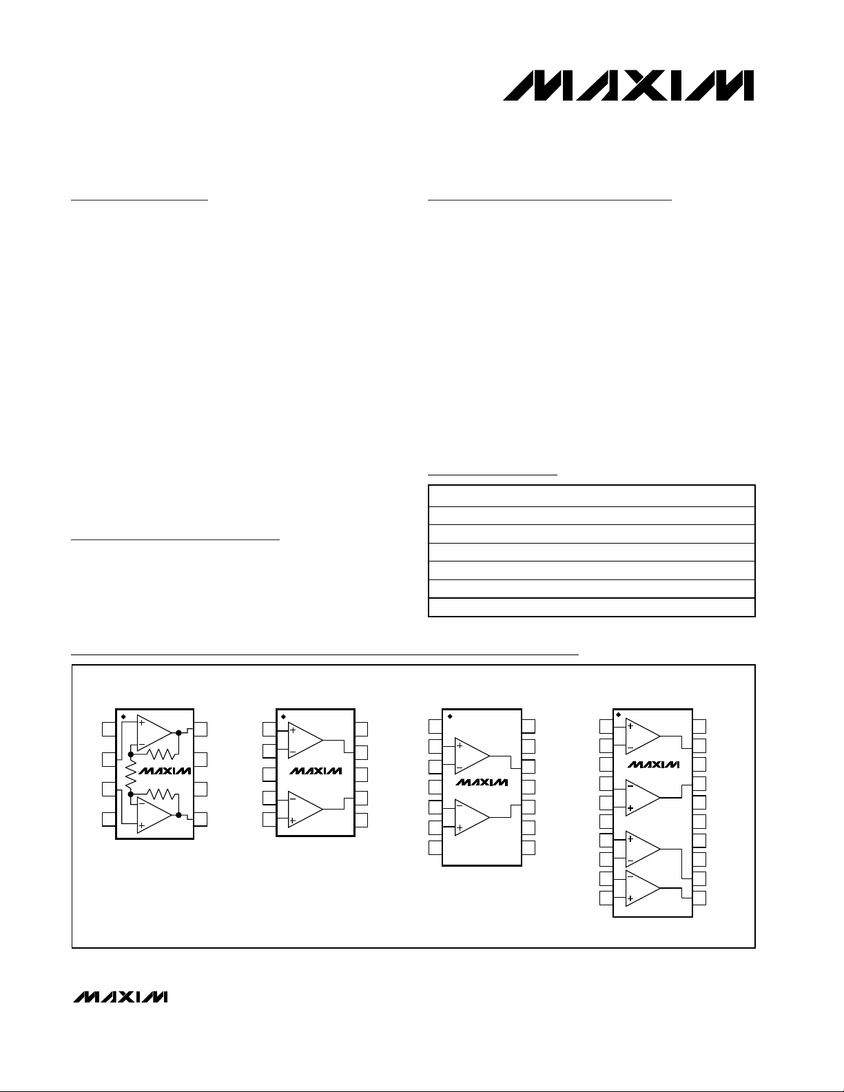
Pin Configurations
Ordering Information
19-2299; Rev 0; 1/02
For pricing, delivery, and ordering information, please contact Maxim/Dallas Direct! at
1-888-629-4642, or visit Maxim’s website at www.maxim-ic.com.
Rail-to-Rail is a registered trademark of Nippon Motorola, Ltd.
PART TEMP RANGE PIN-PACKAGE
MAX4361EUA -40°C to +85°C 8 µMAX
MAX4361ESA -40°C to +85°C 8 SO
MAX4362EUB -40°C to +85°C 10 µMAX
MAX4362ESD -40°C to +85°C 14 SO
MAX4363EUP -40°C to +85°C 20 TSSOP
MAX4363ESP -40°C to +85°C 20 SO
TOP VIEW
1
GND
T1IN+
T1IN-
SHDN
T2IN+
GND
R1IN+
R2IN-
2
3
4
5
6
7
8
9
10
SO/TSSOP
MAX4363
1 8 OUT+GND
27V+IN+
MAX4361 MAX4362
45
µMAX/SO
V+IN- 3 6
OUT-GND
T1IN+
T1IN-
SHDN
1
2
3
4
5
µMAX
10
GND
9
T1OUT
8
V+
7
T2OUTT2IN-
GNDT2IN+
6
T2IN+
MAX4362
SO
141 N.C.N.C.
132 GNDT1IN+
123 T1OUTT1IN-
114V+SHDN
105 T2OUTT2IN-
96
87 N.C.N.C.
20
19
18
17
16
15
14
13
12
11
GND (TX)
T1OUT
V+ (TX)
T2OUTT2IN-
GND (TX)
N.C.
V+ (RX)
GND (RX)R1IN-
R1OUT
R2OUTR2IN+
Page 2
MAX4361/MAX4362/MAX4363
ADSL Drivers/Receivers for Customer Premise
Equipment
2 _______________________________________________________________________________________
ABSOLUTE MAXIMUM RATINGS
ELECTRICAL CHARACTERISTICS—Driver
(V+ = 5V, GND = 0, VCM= 2.5V, RL= 12.5Ω, SHDN = 0, TA= T
MIN
to T
MAX
, unless otherwise noted. Typical values specified at
T
A
= +25°C.)
Stresses beyond those listed under “Absolute Maximum Ratings” may cause permanent damage to the device. These are stress ratings only, and functional
operation of the device at these or any other conditions beyond those indicated in the operational sections of the specifications is not implied. Exposure to
absolute maximum rating conditions for extended periods may affect device reliability.
Supply Voltage (V+ to GND) ....................................-0.3V to +6V
Analog Input Voltage .......................(GND - 0.3V) to (V+ + 0.3V)
SHDN Input Voltage.........................(GND - 0.3V) to (V+ + 0.3V)
Output Short-Circuit Duration .................................................10s
Driver Output Current...............................................................1A
Receiver Output Current ...................................................150mA
Continuous Power Dissipation (T
A
= +70°C)
8-Pin µMAX (derate 4.5mW/°C above +70°C) ..............362mW
10-Pin µMAX (derate 5.6mW/°C above +70°C) ............444mW
8-Pin SO (derate 5.88mW/°C above +70°C).................471mW
14-Pin SO (derate 8.33mW/°C above +70°C)...............667mW
20-Pin SO (derate 10.0mW/°C above +70°C)...............800mW
20-Pin TSSOP (derate 10.9mW/°C above +70°C) ........879mW
Operating Temperature Range ...........................-40°C to +85°C
Junction Temperature......................................................+150°C
Storage Temperature Range .............................-65°C to +150°C
Lead Temperature (soldering, 10s) .................................+300°C
)
PARAMETER SYMBOL CONDITIONS MIN TYP MAX UNITS
S up p l y V ol tag e Rang e ( N ote 1) V
Supply Current I
Maximum Average Output
Power (Notes 2, 3)
Gain G MAX4361 (0.7V ≤ V
Open-Loop Gain A
Second Harmonic Distortion
(Notes 3, 4)
Third Harmonic Distortion
(Notes 3, 4)
Peak Output Current I
Input Offset Voltage V
Input Bias Current I
Input Offset Current I
Differential Input Resistance R
CC
Q
P
OUT
VOL
OUT
OS
B
OS
IN(DIFF
MAX4361, RL = ∞ 22 33 mA
MAX4362, RL = ∞
MAX4363, measured at
V+ (TX), R
MAX4363, measured at
V+ (RX), R
DMT modulation 15.5
CAP modulation 18
MAX4362/MAX4363 (0.7V ≤ V
G = 3.1, f = 100kHz, V
G = 3.1, f = 100kHz, V
Inferred from Output Voltage Swing test 280 330 mA
MAX4361 ±30 ±600
MAX4362/MAX4363 ±10 ±500
MAX4361 25 MΩ
MAX4362/MAX4363 40 kΩ
L
L
= ∞
= ∞
≤ (V+) - 0.7V) 3.0 3.1 3.2 V/V
OUT
OUT(DIFF)
OUT(DIFF)
4.5 5.5 V
SHDN = 0 22 33 mA
SHDN = 5V 60 200 µA
SHDN = 0 22 33 mA
SHDN = 5V 60 200 µA
SHDN = 0 4 6.5 mA
SHDN = 5V 70 200 µA
≤ (V+) - 0.7V) 68 81 dB
OUT
= 7.1V
= 7.1V
P-P
P-P
-66 -76 dBc
-68 -79 dBc
±0.5 ±10 mV
1.6 4.5 µA
dBm
nA
Page 3
MAX4361/MAX4362/MAX4363
ADSL Drivers/Receivers for Customer Premise
Equipment
_______________________________________________________________________________________ 3
ELECTRICAL CHARACTERISTICS—Driver (continued)
(V+ = 5V, GND = 0, VCM= 2.5V, RL= 12.5Ω, SHDN = 0, TA= T
MIN
to T
MAX
, unless otherwise noted. Typical values specified at
T
A
= +25°C.)
)
PARAMETER SYMBOL CONDITIONS MIN TYP MAX UNITS
Input Common-Mode Voltage
Range
Common-Mode Rejection
Ratio
V
CM
Inferred from CMRR test 1.25 4.50 V
CMRR 1.25V ≤ V
CM
≤ 4.5V
Power-Supply Rejection Ratio PSRR V+ = 4.5V to 5.5V
AC Power-Supply Rejection
Ratio
Differential Output-Voltage
Swing (Note 4)
PSRR
V
OU T ( D IF F )
f = 100kHz
AC
Inferred from Output Voltage Swing test 7.4 8.2 V
RL = 100Ω
Output-Voltage Swing
(Note 4)
VOH,
V
OL
MAX4362/MAX4363
= 12.5Ω
R
L
MAX4361, RL = 12.5Ω,
= -20°C to 85°C
T
A
Output Short-Circuit Current I
Output Resistance R
SHDN Logic Low V
SHDN Logic High V
SHDN Input Current IIH, I
Shutdown Output Impedance Z
-3dB Bandwidth BW
Slew Rate SR V
Settling Time (1%) t
Voltage-Noise Density e
Current-Noise Density i
SC
OUT
IL
IH
IL
OUT(SD
S
n
n
MAX4361 0.3
MAX4362/MAX4363, G = 1 0.001
SHDN = 0 or SHDN = V+ ±10 µA
f = 1MHz 1.8 kΩ
MAX4361 40
MAX4362/MAX4363, G = 1 60
OUT(DIFF)
V
OUT(DIFF)
= 7.1V
= 7.1V
step
f = 100kHz to 1.1MHz 4.8 nV /√ Hz
f = 100kHz to 1.1MHz 1.5 p A/√ Hz
Capacitive-Load Stability 10 nF
Shutdown Delay Time t
Enable Delay Time t
SHDN
ENABLE
MAX4361 60 73
MAX4362/MAX4363 70 85
MAX4361 60 89
MAX4362/MAX4363 60 74
MAX4361 63
MAX4362/MAX4363 49
(V+) - V
V
OL
(V+) - V
V
OL
(V+) - V
V
OL
OH
OH
OH
215 550
230 550
400 600
430 650
400 600
430 650
±650 mA
0.8 V
2.0 V
step 30 V/µs
P-P
MAX4361 115
P-P
MAX4362/MAX4363,
G = 3
165
400 ns
2.8 µs
dB
dB
dB
P-P
mV
Ω
MHz
ns
Page 4
MAX4361/MAX4362/MAX4363
ADSL Drivers/Receivers for Customer Premise
Equipment
4 _______________________________________________________________________________________
Note 1: Guaranteed by the Power-Supply Rejection Ratio (PSRR) test.
Note 2: Implied by worst-case output-voltage swing (V
OUT(DIFF)
), crest factor (Cr) and load resistance (RL):
P
Driver
= 10log((250 ✕(V
OUT(DIFF)
)^2 / ((Cr)^2 ✕RL)) dBmW
Note 3: Guaranteed by design.
Note 4: May exceed absolute maximum ratings for power dissipation if unit is subject to full-scale sinusoids for long periods
(see Applications Information section).
ELECTRICAL CHARACTERISTICS—Receiver (MAX4363 only)
(V+ = 5V, GND = 0, VCM= 2.5V, RL= ∞, SHDN = 0, TA= T
MIN
to T
MAX
, unless otherwise noted. Typical values specified at
T
A
= +25°C.)
)
,
PARAMETER SYMBOL CONDITIONS MIN TYP MAX UNITS
Spurious-Free Dynamic Range SFDR G = 1, f = 1MHz, V
Gain-Bandwidth Product GBW 190 MHz
Open-Loop Gain A
Peak Output Current I
Input Offset Voltage V
Input Bias Current I
Input Offset Current I
Input Capacitance C
Differential Input Resistance R
IN(DIFF
Input Common-Mode Voltage
Range
Common-Mode Rejection Ratio C
VOL
OUT
OS
V
MRR
OS
B
IN
CM
1.5V ≤ V
OUT
RL = 50Ω, inferred from Output-Voltage
Swing test
Inferred from CMRR test 0.25 3.80 V
0.25V ≤ VCM ≤ 3.8V 70 87 dB
Power-Supply Rejection Ratio PSRR V+ = 4.5V to 5.5V 60 75 dB
AC Power-Supply Rejection
Ratio
PSRR
f = 1MHz 47 dB
AC
RL = ∞
Output-Voltage Swing V
OH
V
OL
RL = 50Ω
Output Short-Circuit Current I
Output Resistance R
Slew Rate SR V
Settling Time (1%) t
Voltage-Noise Density e
Current-Noise Density i
Driver-Receiver Crosstalk X
SC
OUT
S
n
n
TALK
G = 1 0.001 Ω
= 1V
V
OUT
OUT
P-P
= 100mV
f = 1MHz 8.5 nV/√Hz
f = 1MHz 0.5 pA/√Hz
f = 100kHz 95 dB
OUT
= 1V
P-P
-75 dBc
≤ 3.5V 65 77 dB
18 25 mA
±0.5 ±10 mV
-0.75 -2 µA
±20 ±250 nA
1.6 pF
76 kΩ
(V+) - V
V
OL
(V+) - V
V
OL
OH
OH
0.64 1
0.73 1
1.27 1.5
1.37 1.6
±130 mA
step 160 V/µs
step, G = 1 40 ns
P-P
V
Page 5

MAX4361/MAX4362/MAX4363
ADSL Drivers/Receivers for Customer Premise
Equipment
_______________________________________________________________________________________ 5
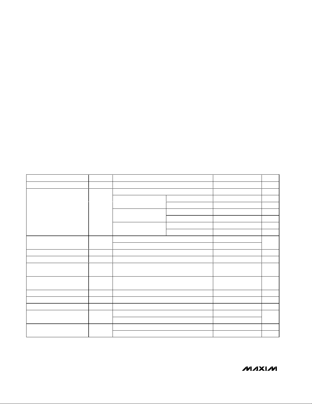
Typical Operating Characteristics
(V+ = 5V, GND = 0, VCM= 2.5V, RL= 12.5Ω, SHDN = 0, TA= +25°C.)
DRIVER DIFFERENTIAL DISTORTION
vs. FREQUENCY
-40
V
= 7.2V
OUT
P-P
G = 3
-50
= 12.5Ω
R
L
-60
2ND HARMONIC
-70
-80
DIFFERENTIAL DISTORTION (dB)
-90
-100
10k 1M
FREQUENCY (Hz)
3RD HARMONIC
100k
DRIVER LINE POWER
vs. TURNS RATIO
16.0
15.5
15.0
14.5
14.0
13.5
(dBm)
13.0
LINE
P
12.5
12.0
11.5
11.0
10.5
10.0
3.0 5.0
V+ = 5.5V
V+ = 5V
V+ = 4.5V
TRANSFORMER TURNS RATIO
DRIVER GAIN AND PHASE
vs. FREQUENCY
20
15
10
5
0
-5
GAIN (dB)
-10
-15
-20
-25
-30
10k 1G
GAIN
PHASE
FREQUENCY (Hz)
MAX4361 toc07
G = 3
= 12.5Ω
R
L
100M10M1M100k
MAX4361 toc01
MAX4361 toc04
4.84.64.2 4.43.4 3.6 3.8 4.03.2
120
90
60
30
0
-30
-60
PHASE (DEGREES)
-90
-120
-150
-180
DRIVER DIFFERENTIAL DISTORTION
vs. PEAK-TO-PEAK OUTPUT VOLTAGE
-40
f = 100kHz
G = 3
-50
= 12.5
W
R
L
-60
-70
-80
DIFFERENTIAL DISTORTION (dBc)
-90
-100
28
PEAK-TO-PEAK OUTPUT VOLTAGE (V)
DRIVER CURRENT AND VOLTAGE NOISE
vs. FREQUENCY
100
10
INPUT CURRENT NOISE (pA/√Hz)
1
DRIVER POWER-SUPPLY REJECTION
RATIO vs. FREQUENCY
10
G = 1
0
-10
-20
-30
-40
PSRR (dB)
-50
-60
-70
-80
1k 1G
3RD HARMONIC
2ND HARMONIC
FREQUENCY (Hz)
FREQUENCY (Hz)
DRIVER DIFFERENTIAL DISTORTION
-60
MAX4361 toc02
76543
MAX4361 toc05
100
10
V
NOISE
I
NOISE
100k10k
10M1M100k10k
1M1k
1
MAX4361 toc08
-70
-80
-90
DIFFERENTIAL DISTORTION (dBc)
-100
100k
10k
1k
100
10
1
OUTPUT IMPEDANCE (Ω)
INPUT VOLTAGE NOISE (nV/√Hz)
0.1
0.01
100k 100M
2.5
2.4
2.3
2.2
2.1
2.0
1.9
1.8
1.7
1.6
OUTPUT SWING (V)
1.5
1.4
1.3
1.2
1.1
1.0
vs. LOAD RESISTANCE
V
= 5V
OUT
P-P
f = 100kHz
G = 3
= 12.5Ω
R
L
3RD HARMONIC
2ND HARMONIC
5
R
(Ω)
LOAD
85654525
DRIVER OUTPUT IMPEDANCE
vs. FREQUENCY
SHDN = V
CC
SHDN = GND
10M1M
FREQUENCY (Hz)
DRIVER OUTPUT SWING
vs. LOAD RESISTANCE
+SWING
-SWING
1 10k
LOAD RESISTANCE (Ω)
1k10010
MAX4361 toc03
MAX4361 toc06
MAX4361 toc09
Page 6

MAX4361/MAX4362/MAX4363
ADSL Drivers/Receivers for Customer Premise
Equipment
6 _______________________________________________________________________________________
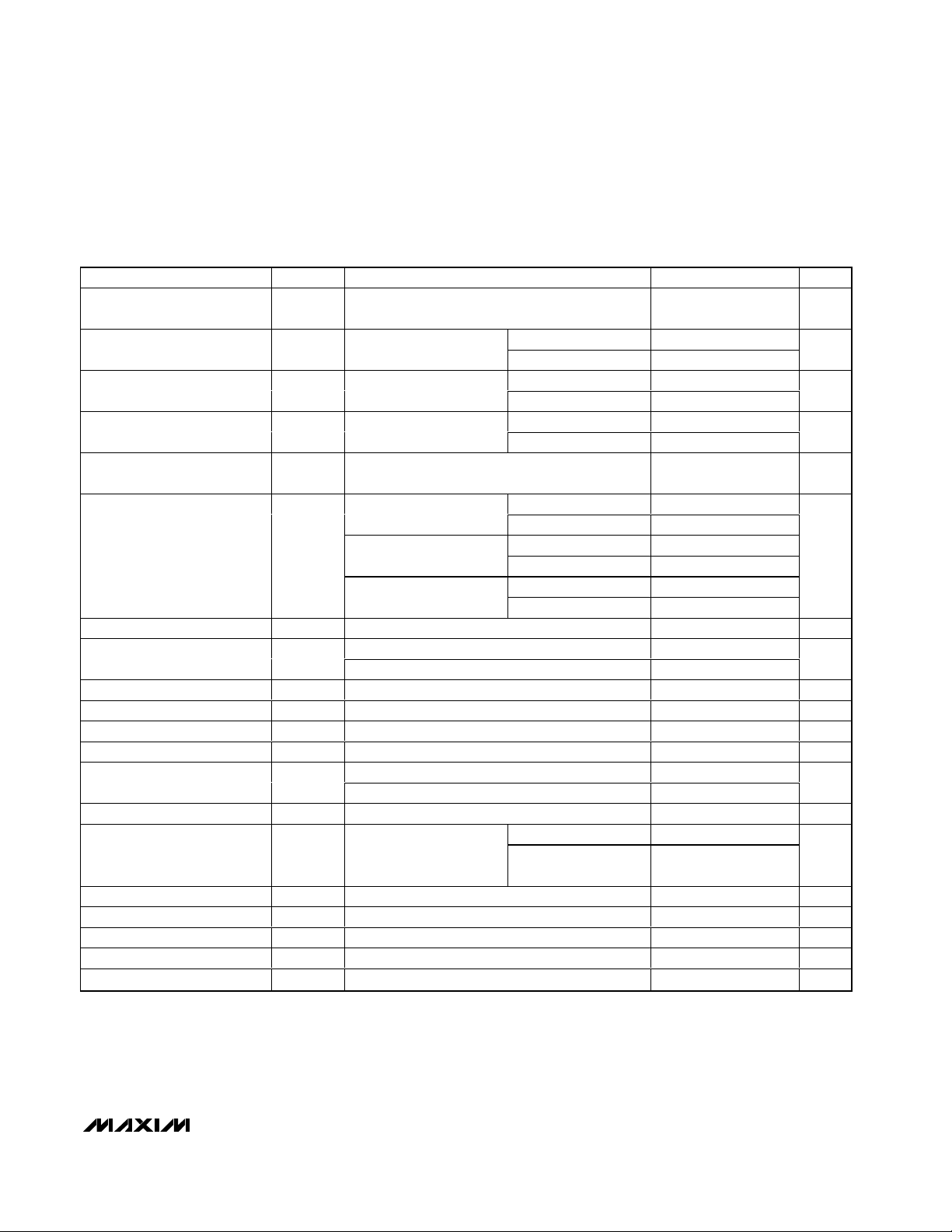
Typical Operating Characteristics (continued)
(V+ = 5V, GND = 0, VCM= 2.5V, RL= 12.5Ω, SHDN = 0, TA= +25°C.)
MAX4361 toc010
FREQUENCY (Hz)
DIFFERENTIAL DISTORTION (dB)
100k
-90
-80
-70
-60
-50
-40
-100
10k 1M
RECEIVER DIFFERENTIAL DISTORTION
vs. FREQUENCY
3RD HARMONIC
2ND HARMONIC
V
OUT
= 1V
P-P
G = 1
R
L
= 150Ω
FREQUENCY (Hz)
100k10k
1
1M1k
100
0.1
1
10 10
100
0.1
MAX4361 toc11
RECEIVER CURRENT AND VOLTAGE
NOISE vs. FREQUENCY
INPUT CURRENT NOISE (pA/√Hz)
INPUT VOLTAGE NOISE (nV/√Hz)
V
NOISE
I
NOISE
RECEIVER GAIN AND PHASE
vs. FREQUENCY
MAX4361 toc12
FREQUENCY (Hz)
GAIN (dB)
100M10M1M100k
-20
-10
0
10
20
30
40
50
60
70
-30
10k 1G
GAIN
PHASE
G = 1000
R
L
= 500Ω
PHASE (DEGREES)
-150
-120
-90
-60
-30
0
30
60
90
120
-180
MAX4361 toc13
FREQUENCY (Hz)
PSRR (dB)
10M1M100k10k
-70
-60
-50
-40
-30
-20
-10
0
10
-80
1k 100M
RECEIVER POWER-SUPPLY REJECTION
RATIO vs. FREQUENCY
G = 1
DRIVER-TO-RECEIVER CROSSTALK
vs. FREQUENCY
MAX4361 toc14
FREQUENCY (Hz)
CROSSTALK (dB)
100M10M1M100k
-100
-80
-60
-40
-20
0
-120
10k 1G
RL = 12.5Ω
NO LOAD
RECEIVER-TO-RECEIVER CROSSTALK
vs. FREQUENCY
MAX4361 toc15
FREQUENCY (Hz)
CROSSTALK (dB)
100M10M1M100k
-100
-80
-60
-40
-20
0
-120
10k 1G
NO LOAD
RL = 150Ω
RECEIVER OUTPUT AMPLITUDE
vs. FREQUENCY
MAX4361 toc16
FREQUENCY (Hz)
100M10M1M100k
-8
-6
-4
-2
0
2
4
-10
10k 1G
RF = 100Ω
RF = 1kΩ
RF = 500Ω
G = -1
R
L
= 150Ω
V
P-P
= 100mV
GAIN (dB)
Page 7

MAX4361/MAX4362/MAX4363
ADSL Drivers/Receivers for Customer Premise
Equipment
_______________________________________________________________________________________ 7
Pin Descriptions
MAX4361
MAX4362
PIN NAME FUNCTION
1, 4 GND Ground
2 IN+ First Driver Input
3 IN- Second Driver Input
5 OUT- Second Driver Output
6, 7 V+ Positive Power-Supply Voltage. Bypass V+ to GND with a 0.1µF capacitor.
8 OUT+ First Driver Output
µMAX SO
PIN
1 2 T1IN+ First Driver Noninverting Input
2 3 T1IN- First Driver Inverting Input
3 4 SHDN Shutdown. Connect to GND for normal operation.
4 5 T2IN- Second Driver Inverting Input
5 6 T2IN+ Second Driver Noninverting Input
6, 10 9, 13 GND Ground
7 10 T2OUT Second Driver Output
8 11 V+ Positive Power-Supply Voltage. Bypass V+ to GND with a 0.1µF capacitor.
9 12 T1OUT First Driver Output
— 1, 7, 8, 14 N.C. No Connection. Not internally connected.
NAME FUNCTION
Page 8

MAX4361/MAX4362/MAX4363
ADSL Drivers/Receivers for Customer Premise
Equipment
8 _______________________________________________________________________________________
Detailed Description
The MAX4361/MAX4362/MAX4363 are a family of highperformance ADSL drivers and drivers/receivers ideal
for the upstream transmit path and the downstream
receive path of customer premise equipment. These
devices operate from a single 5V supply and deliver up
to 12.5dBm average line power for DMT modulated signals, meeting the requirements of full-rate ADSL. SFDR
at full output power is typically -75dBc at 100kHz.
Differential In/Differential Out ADSL Driver
(MAX4361)
The MAX4361 is a differential line driver with a fixed
gain of 3.1V/V. The gain is set by three internal resistors.
Uncommitted Dual Amplifier for ADSL
Driver (MAX4362)
The MAX4362 is a dual amplifier with shutdown intended for use as a differential IN/differential OUT driver
with gain set with external resistors
Uncommitted Quad Amplifier for ADSL
Driver/Receiver (MAX4363)
The MAX4363 is a quad amplifier with shutdown intended
for use as a differential IN/differential OUT driver/receiver
combination with gain set with external resistors.
Shutdown
The MAX4362/MAX4363 feature a low-power shutdown
mode. When the SHDN pin is pulled high, the supply
current drops to 70µA, and the amplifier’s outputs are
placed in a high-impedance disable mode. Connect
SHDN to GND for normal operation.
MAX4363
Pin Descriptions (continued)
PIN NAME FUNCTION
1 T1IN+ First Driver Noninverting Input
2 T1IN- First Driver Inverting Input
3 SHDN Shutdown. Connect to GND for normal operation.
4 T2IN- Second Driver Inverting Input
5 T2IN+ Second Driver Noninverting Input
6 GND Ground
7 R1IN+ First Receiver Noninverting Input
8 R1IN- First Receiver Inverting Input
9 R2IN- Second Receiver Inverting Input
10 R2IN+ Second Receiver Noninverting Input
11 R2OUT Second Receiver Output
12 R1OUT First Receiver Output
13 GND (RX) Ground for Receiver Amplifiers
14 V+ (RX)
15 N.C. No Connection. Not internally connected.
16, 20 GND (TX) Ground for Driver Amplifier
17 T2OUT Second Driver Output
18 V+ (TX)
19 T1OUT First Driver Output
Positive Power-Supply Voltage for Receiver Amplifiers. Bypass V+ (RX) to GND (RX) with a
separate 0.1µF capacitor.
Positive Power-Supply Voltage for Driver Amplifiers. Bypass V+ (TX) to GND (TX) with a
separate 0.1µF capacitor.
Page 9

MAX4361/MAX4362/MAX4363
ADSL Drivers/Receivers for Customer Premise
Equipment
_______________________________________________________________________________________ 9
Applications Information
Power Supply and Decoupling
The MAX4361/MAX4362/MAX4363 should be powered
from a well-regulated, low-noise, 4.5V to 5.5V supply in
order to optimize the ADSL upstream drive capability to
+12.5dBm and maintain the best SFDR.
High-quality capacitors with low equivalent series resistance (ESR) such as multilayer ceramic capacitors
(MLCCs) should be used to minimize supply voltage
ripple and power dissipation. A larger capacitor located
in proximity to the MAX4361/MAX4362/MAX4363
improves decoupling for lower frequency signals.
In addition, 0.1µF MLCC decoupling capacitors should
be located as close as possible to each of the powersupply pins, no more than 1/8 inch away. An additional
large (4.7µF to 10µF) tantalum capacitor should be
placed on the board near the supply terminals to supply current for fast, large-signal changes at the
MAX4361/MAX4362/MAX4363 outputs.
MAX4361/MAX4362
The MAX4361/MAX4362 require a single 0.1µF bypass
from V+ to ground located as close as possible to the
IC leads.
MAX4363
The MAX4363 features separate supply and ground
pins for the receiver and driver amplifiers. Bypass the
V+ (RX) supply to the GND (RX) pin with a 0.1µF capacitor. Bypass the V+ (TX) supply to the GND (TX) pin with
a separate 0.1µF capacitor. Both capacitors should be
placed as close as possible to their respective IC leads.
USB Applications
The 5V supplied at the universal serial bus (USB) port
may be poorly regulated or unable to supply the peak
currents required by an ADSL modem. Improving the
quality of the supply will optimize the performance of
the MAX4361/MAX4362/MAX4363 in a USB-supplied
CPE ADSL modem. This can be accomplished through
the use of a step-up DC-to-DC converter or switching
power supply followed by a low-dropout (LDO) regulator. Careful attention must be paid to decoupling the
power supply at the output of the DC-to-DC converter,
the output of the LDO regulator and the supply pins of
the MAX4361/MAX4362/MAX4363.
Driving a Capacitive Load
The MAX4361/MAX4362/MAX4363 are capable of driving capacitive loads up to 2nF. Most hybrid circuits
are well under this limit. For additional capacitive-drive
capability use isolation resistors between the output
and the load to reduce ringing on the output signal. In a
typical hybrid the back-matching resistors provide sufficient isolation for most any capacitive-loading condition
(see Figure 1).
Method for Generating a Midsupply
Voltage
To operate an amplifier on a single-voltage supply, a
voltage midway between the supply and ground must be
generated to properly bias the inputs and the outputs.
A voltage divider can be created with two equal-value
resistors (Figure 2). There is a trade-off between the
power consumed by the divider and the voltage drop
across these resistors due to the positive input bias
currents. Selecting 2.7kΩ for R1 and R2 will create a
voltage divider that draws less than 1mA from a 5V
supply. Use a decoupling capacitor (0.1µF) at the node
where V
REF
is generated.
Power Dissipation
It is important to consider the total power dissipation of
the MAX4361/MAX4362/MAX4363 in order to properly
size the heat sink area of an application. With some
simplifying assumptions we can estimate the total
power dissipated in the driver (see Typical Operating
Figure 2. Voltage-Divider Reference
Figure 1. Driving Capacitive Load
500Ω
INPUT
2.7kΩ
2.7kΩ
1kΩ
MAX436 _
5V
R1
R2
3.1Ω
0.1µF
OUTPUT
C
LOAD
V
REF
Page 10

MAX4361/MAX4362/MAX4363
ADSL Drivers/Receivers for Customer Premise
Equipment
10 ______________________________________________________________________________________
Circuit). If the output current is large compared to the
quiescent current, computing the dissipation in the output devices and adding it to the quiescent power dissipation will give a close approximation of the total power
dissipation in the package.
For a 12.5dBm average line power on a 100Ω line, the
RMS current is 13.4mA. With a one-to-four transformer
the driver therefore supplies 53.6mA RMS. It can be
shown for a DMT signal the ratio of RMS current to the
average rectified current is 0.8. The total power consumption is approximately
P
CONS
= 0.8 ✕ 53.6 x 5V = 214mW
of which 18mW is delivered as line power and 18mW is
dissipated in the back-matching resistors. Hence the
average power consumption of the IC is approximately
178mW + quiescent power (110mW), or 288mW. For
the MAX4361 in an 8-pin µMAX package, this corresponds to a temperature rise of 64°C. With an ambient
temperature of +85°C this corresponds to a junction
temperature of +148°C, just below the absolute maximum of +150°C.
Please note the part is capable of over 200mA RMS,
which could cause thermal shutdown in applications
with elevated ambient temperatures and/or signals with
low crest factors. See Figure 3 for a guide to power derating for each of the MAX4361/MAX4362/MAX4363
packages.
Transformer Selection
Full-rate, customer premise ADSL requires the transmission of a +12.5dBm (18mW) DMT signal. The DMT
signal has a typical crest factor of 5.3, requiring the line
driver to provide peak line power of 27.5dBm (560mW).
The 27.5dBm peak line power translates into a 28.4V
peak-to-peak differential voltage on the 100Ω telephone
line. The maximum low-distortion output swing available
from the MAX4361/MAX4362/MAX4363 line driver on a
5V supply is 3.8V and, taking into account the power
lost due to the back-matching resistance, a step-up
transformer with turns ratio of 3.8 or greater is needed.
In the Typical Operating Circuit, the MAX4363 is coupled to the phone line through a step-up transformer
with a 1:4 turns ratio. R1 and R2 are back-matching
resistors, each 3.1Ω (100Ω / (2 ✕ 42)), where 100Ω is
the approximate phone-line impedance. The total differential load for the MAX4361/MAX4362/MAX4363,
including the termination resistors, is therefore 12.5Ω.
Even under these conditions the MAX4361/MAX4362/
MAX4363 provide low distortion signals to within 0.6V of
the power rails.
Receive Channel Considerations
A transformer used at the output of the differential line
driver to step up the differential output voltage to the line
has the inverse effect on signals received from the line.
A voltage reduction or attenuation equal to the inverse of
the turns ratio is realized in the receive channel of a typical bridge hybrid. The turns ratio of the transformer may
also be dictated by the ability of the receive circuitry to
resolve low-level signals in the noisy, twisted-pair telephone plant. Higher turns-ratio transformers effectively
reduce the received signal-to-noise ratio due to the
reduction in the received signal strength.
The MAX4363 includes an amplifier with typical voltage
noise of only 8.5nV/√Hz and a low-supply current of
2mA/amplifier to be used as the receive channel.
Layout Considerations
Good layout techniques optimize performance by
decreasing the amount of stray capacitance at the
amplifier’s inputs and outputs. Excess capacitance will
produce peaking in the amplifier’s frequency response.
To decrease stray capacitance, minimize trace lengths
by placing external components as close to the amplifier as possible.
Chip Information
MAX4361 TRANSISTOR COUNT: 1400
MAX4362 TRANSISTOR COUNT: 1400
MAX4363 TRANSISTOR COUNT: 1750
PROCESS: Bipolar
Figure 3. Maximum Power Dissipation vs. Temperature
2.5
2.0
1.5
1.0
0.5
MAXIMUM POWER DISSIPATION (W)
0
-40 0-20 20 40 60 80
MAX4361
8-PIN µMAX
MAX4362
14-PIN SO
MAX4363
20-PIN SO
MAX4362
10-PIN µMAX
TEMPERATURE (
MAX4363
20-PIN TSSOP
MAX4361
8-PIN SO
°C)
Page 11

MAX4361/MAX4362/MAX4363
ADSL Drivers/Receivers for Customer Premise
Equipment
______________________________________________________________________________________ 11
Typical Operating Circuit
ADSL
CHIPSET
2.7kΩ
2.7kΩ
0.047µF
0.047µF
5V
V
CC
DRIVER
0.1µF
OUT+
OUT-
IN1IN1+
IN2+
IN2-
1kΩ
3.125Ω
LINE IMPEDANCE
3.125Ω
TRANSFORMER
500Ω
1kΩ
500Ω
5V
100Ω
1:4
5V
1kΩ
1kΩ
0.1µF
10kΩ
IN1+
IN1-
10kΩ
1kΩ
IN2-
IN2+
OUT+
OUT-
MAX4363
5V
RECEIVER
10kΩ
GND
1kΩ
1kΩ
10kΩ
0.1µF
Page 12

MAX4361/MAX4362/MAX4363
ADSL Drivers/Receivers for Customer Premise
Equipment
12 ______________________________________________________________________________________
Package Information
8LUMAXD.EPS
10LUMAX.EPS
Page 13

MAX4361/MAX4362/MAX4363
ADSL Drivers/Receivers for Customer Premise
Equipment
Maxim cannot assume responsibility for use of any circuitry other than circuitry entirely embodied in a Maxim product. No circuit patent licenses are
implied. Maxim reserves the right to change the circuitry and specifications without notice at any time.
Maxim Integrated Products, 120 San Gabriel Drive, Sunnyvale, CA 94086 408-737-7600 ____________________ 13
© 2002 Maxim Integrated Products Printed USA is a registered trademark of Maxim Integrated Products.
Package Information (continued)
SOICN.EPS
 Loading...