

General Description
The MAX4356 is a 16 ✕ 16 highly integrated video
crosspoint switch matrix with input and output buffers
and On-Screen Display (OSD) Insertion. This device
operates from dual ±3V to ±5V supplies or from a single +5V supply. Digital logic is supplied from an independent single +2.7V to +5.5V supply. Individual
outputs can be switched between an input video signal
source and OSD information through an internal, dedicated fast 2:1 mux (40ns switching times) located
before the output buffer. All inputs and outputs are
buffered, with all outputs able to drive standard 75Ω
reverse-terminated video loads.
The switch matrix configuration and output buffer gain
are programmed via an SPI/QSPI™-compatible, threewire serial interface and initialized with a single update
signal. The unique serial interface operates in two
modes facilitating both fast updates and initialization.
On power-up, all outputs are initialized in the disabled
state to avoid output conflicts in large-array configurations.
Superior flexibility, high integration, and space-saving
packaging make this nonblocking switch matrix ideal
for routing video signals in security and video-ondemand systems.
The MAX4356 is available in a 128-pin TQFP package
and specified over an extended -40°C to 85°C temperature range.
Applications
Security Systems
Video Routing
Video-on-Demand Systems
Features
♦ 16 ✕16 Nonblocking Matrix with Buffered Inputs
and Outputs
♦ Operates from ±3V, ±5V, or +5V Supplies
♦ Individually Programmable Output Buffer Gain
(A
V
= +1V/V or +2V/V)
♦ High-Impedance Output Disable for Wired-OR
Connections
♦ Fast-Switching (40ns) 2:1 OSD Insertion Mux
♦ 0.1dB Gain Flatness to 14MHz
♦ -62dB Crosstalk, -110dB Isolation at 6MHz
♦ 0.02%/0.12° Differential Gain/Differential Phase
Error
♦ Low 195mW Power Consumption (0.76mW per
Point)
MAX4356
16 x 16 Nonblocking Video Crosspoint Switch
with On-Screen Display Insertion and I/O Buffers
________________________________________________________________ Maxim Integrated Products 1
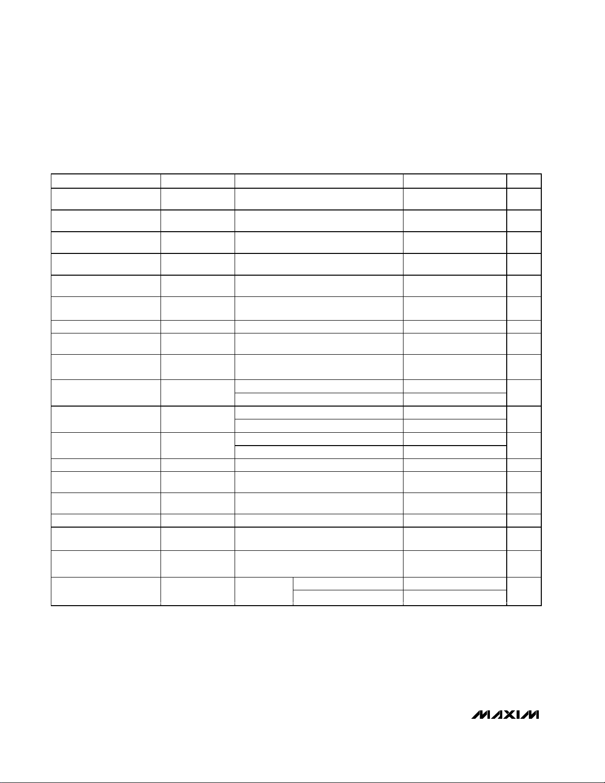
Ordering Information
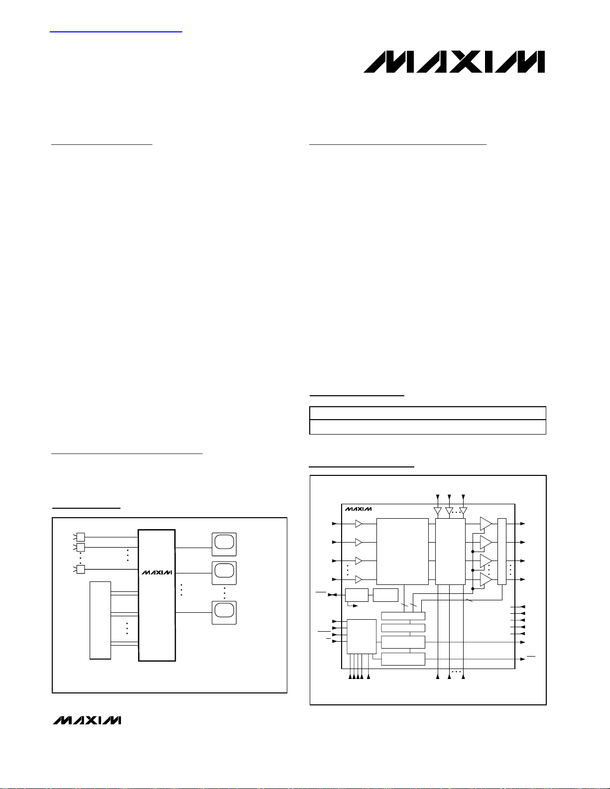
OUT0
OSDFILL0
OSDKEY0
OSDFILL1
OSDKEY1
OSDFILL15
OSDKEY15
OUT1
OUT15
IN0
CAMERAS
IN1
IN15
MONITOR
MONITOR
MONITOR
MAX4356
OSD GENERATOR
MAX4356
16 x 16
SWITCH MATRIX
POWER-ON
RESET
SERIAL
INTERFACE
THERMAL
SHUTDOWN
DECODE LOGIC
DISABLE ALL OUTPUTS
LATCHES
256
16
16
MATRIX REGISTER
96 BITS
UPDATE REGISTER
16 BITS
2:1
OSD
MUX
ENABLE/DISABLE
AV*
AV*
AV*
AV*
*AV = +1V/V OR +2V/V
A0-A3 MODE
IN0
IN1
IN2
IN15
DIN
SCLK
UPDATE
CE
RESET
OSDKEY0 OSDKEY15
OSDKEY1
OSDFILL0 OSDFILL15
OUT0
OUT1
OUT2
OUT15
V
CC
V
EE
DGND
V
DD
DOUT
AOUT
OSDFILL1
AGND
Typical Operating Circuit
Functional Diagram
19-2113; Rev 0; 8/01
For pricing, delivery, and ordering information, please contact Maxim/Dallas Direct! at
1-888-629-4642, or visit Maxim’s website at www.maxim-ic.com.
SPI and QSPI are trademarks of Motorola, Inc.
Pin Configuration appears at end of data sheet.
查询MAX4356ECD供应商
PART TEMP. RANGE PIN-PACKAGE
MAX4356ECD -40°C to +85°C 128 TQFP
MAX4356
16 x 16 Nonblocking Video Crosspoint Switch
with On-Screen Display Insertion and I/O Buffers
2 _______________________________________________________________________________________
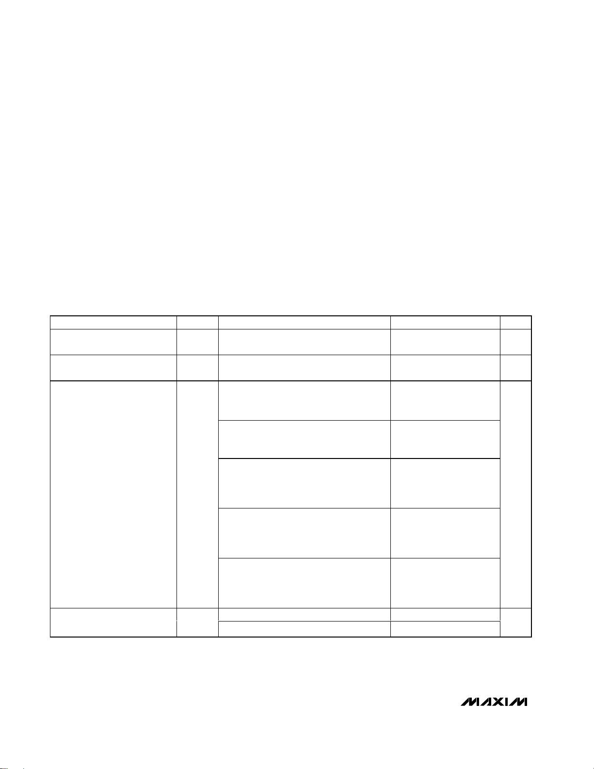
ABSOLUTE MAXIMUM RATINGS
DC ELECTRICAL CHARACTERISTICS—DUAL SUPPLIES ±5V
(VCC= +5V, VEE= -5V, VDD= +5V, AGND = DGND = 0, VIN_= 0, V
OSDFILL
_ = 0, RL= 150Ω to AGND, and TA= T
MIN
to T
MAX
,
unless otherwise noted. Typical values are at T
A
= +25°C.)
Stresses beyond those listed under “Absolute Maximum Ratings” may cause permanent damage to the device. These are stress ratings only, and functional
operation of the device at these or any other conditions beyond those indicated in the operational sections of the specifications is not implied. Exposure to
absolute maximum rating conditions for extended periods may affect device reliability.
Analog Supply Voltage (VCC- VEE) .....................................+11V
Digital Supply Voltage (V
DD
- DGND) ...................................+6V
Analog Supplies to Analog Ground
(V
CC
- AGND) and (AGND - VEE) ......................................+6V
Analog Ground to Digital Ground .........................-0.3V to +0.3V
IN_, OSDFILL_ Voltage Range........ (V
CC
+ 0.3V) to (VEE- 0.3V)
OUT_ Short-Circuit Duration to AGND, V
CC
, or VEE......Indefinite
SCLK, CE, UPDATE, MODE, A_, DIN, DOUT,
RESET, AOUT, OSDKEY_.......(V
DD
+ 0.3V) to (DGND - 0.3V)
Current into Any Analog Input Pin (IN_, OSDFILL_) .........±50mA
Current into Any Analog Output Pin (OUT_).....................±75mA
Continuous Power Dissipation (T
A
= +70°C)
128-Pin TQFP (derate 25mW/°C above +70°C).................2W
Operating Temperature Range ...........................-40°C to +85°C
Junction Temperature......................................................+150°C
Storage Temperature Range .............................-65°C to +150°C
Lead Temperature (soldering, 10s) ................................ +300°C
Operating Supply Voltage
Range
Logic Supply Voltage Range
PARAMETER SYMBOL
V
CC
V
EE
VDD to
DGND
Guaranteed by PSRR test
CONDITIONS
MIN
4.5
2.7
TYP
MAX UNITS
10.5
5.5
V
V
Gain (Note 1)
Gain Matching
(Channel to Channel)
(VEE + 2.5V) < V
= +1V/V, RL = 150Ω
A
V
(VEE + 2.5V) < V
= +1V/V, RL = 10kΩ
A
V
(VEE + 3.75V) < V
A
AV = +2V/V, RL = 150Ω
V
(VEE + 3.75V) < V
AV = +2V/V, RL = 10kΩ
(VEE + 1V) < V
AV = +1V/V, RL = 10kΩ
RL = 10kΩ
RL = 150Ω
< (VCC - 2.5V),
IN
_
< (VCC - 2.5V),
IN
_
< (VCC - 3.75V),
IN
_
< (VCC - 3.75V)
IN
_
< (VCC - 1.2V),
IN
_
0.97 0.995
0.99 0.999
1.92 1.996
1.94 2.008
0.95 0.994
0.5
0.5
1
1
2.08
2.06
1
1.5
2
V/V
%

MAX4356
16 x 16 Nonblocking Video Crosspoint Switch
with On-Screen Display Insertion and I/O Buffers
_______________________________________________________________________________________ 3
DC ELECTRICAL CHARACTERISTICS—DUAL SUPPLIES ±5V (continued)
(VCC= +5V, VEE= -5V, VDD= +5V, AGND = DGND = 0, VIN_= 0, V
OSDFILL
_ = 0, RL= 150Ω to AGND, and TA= T
MIN
to T
MAX
,
unless otherwise noted. Typical values are at T
A
= +25°C.)
Temperature Coefficient of Gain TC
Input Voltage Range
Output
Voltage Range
Input Bias Current
Input Resistance
Output Offset Voltage
PARAMETER SYMBOL
VIN_
V
OUT
I
B
R
IN
V
OFFSET
AV
_
AV = +1V/V
AV = +2V/V
RL = 10kΩ
RL = 150Ω
(VEE + 1V) < V
AV = +1V/V
AV = +2V/V
CONDITIONS
RL = 10kΩ
RL = 150Ω
RL = 10kΩ
RL = 150Ω
< (VCC - 1.2V)
IN
_
MIN
V
+ 1
E E
V
+
E E
2.5
V
+
E E
3
V
+
E E
3.75
V
+
E E
1
V
+
E E
2.5
10
±5
TYP
10
4
±10
MAX UNITS
V
-
C C
1.2
V
-
C C
2.5
V
-
C C
3.1
V
-
C C
3.75
V
-
C C
1.2
V
-
C C
2.5
11
±20
±40
ppm/°C
V
V
V
µA
MΩ
mV
Output Short-Circuit Current
Enabled Output Impedance
Output Leakage Current,
Disable Mode
DC Power-Supply Rejection
Ratio
Quiescent
Supply Current
I
SC
Z
OUT
I
OD
PSRR 4.5V < (V
I
CC
I
EE
I
DD
Sinking or sourcing, RL = 1Ω
(VEE + 1V) < V
(VEE + 1V) < V
RL = ∞
RL = ∞
< (VCC - 1.2V)
IN
_
OUT
- VEE) < 10.5V
CC
< (VCC - 1.2V)
_
Outputs enabled,
= +25°C
T
A
Outputs enabled
Outputs disabled
Outputs enabled,
= +25°C
T
A
Outputs enabled
Outputs disabled
±40
60
0.2
0.004
70
110
60
105
55
4
1
160
185
80
160
185
80
8
mA
Ω
µA
dB
mA
MAX4356
16 x 16 Nonblocking Video Crosspoint Switch
with On-Screen Display Insertion and I/O Buffers
4 _______________________________________________________________________________________
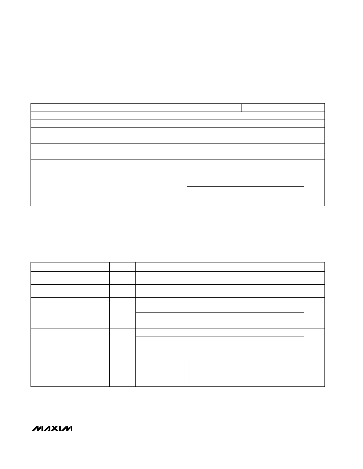
DC ELECTRICAL CHARACTERISTICS—DUAL SUPPLIES ±3V
(VCC= +3V, VEE= -3V, VDD= +3V, AGND = DGND = 0, VIN_ = 0, V
OSDFILL
_ = 0, RL= 150Ω to AGND, and TA= T
MIN
to T
MAX
,
unless otherwise noted. Typical values are at T
A
= +25°C.)
Operating Supply Voltage
Range
Logic Supply Voltage Range
PARAMETER SYMBOL CONDITIONS MIN TYP MAX UNITS
V
- V
CC
V
DD
DGND
Gain (Note 1) A
Gain Matching
(Channel to Channel)
Temperature Coefficient of
Gain
Input Voltage Range V
Output Voltage Range V
Input Bias Current I
Input Resistance R
Output Offset
Voltage
TC
OUT
V
OFFSET
IN
B
IN
Guaranteed by PSRR test 4.5 10.5 V
EE
to
(V
+ 1V) < V
EE
A
= +1V/V, RL = 150Ω
V
(V
+ 1V) < V
EE
A
= +1V/V, RL = 10kΩ
V
AV
_
V
(V
+ 2V) < V
EE
= +2V/V, RL = 150Ω
A
V
(V
+ 2V) < V
EE
= +2V/V, RL = 10kΩ
A
V
R
= 10kΩ 0.5 1.5
L
RL = 150Ω 0.5 2
10 ppm/°C
AV = +1V/V
A
= +2V/V
V
R
= 10kΩ
L
R
= 150Ω
L
(V
+ 1V) < V
EE
A
= +1V/V ±5 ±20
V
A
= +2V/V ±10 ±40
V
< (VCC - 1.2V),
IN
_
< (VCC - 1.2V),
IN
_
< (VCC - 2.1V),
IN
_
< (VCC - 2.1V)
IN
_
< (VCC - 1.2V) 10 MΩ
IN
_
2.7 5.5 V
0.94 0.983 1
0.96 0.993 1
1.92 1.985 2.08
1.94 2.000 2.06
RL = 10kΩ
R
= 150Ω
L
R
= 10kΩ
L
R
= 150Ω
L
+
EE
1
V
+
EE
1
V
+
EE
2
V
+
EE
2
V
+
EE
1
V
+
EE
1
VCC -
1.2
VCC -
1.2
VCC -
2.1
VCC -
2.1
VCC -
1.2
VCC -
1.2
V
4 11 µA
V/V
%
V
V
mV
MAX4356
16 x 16 Nonblocking Video Crosspoint Switch
with On-Screen Display Insertion and I/O Buffers
_______________________________________________________________________________________ 5
DC ELECTRICAL CHARACTERISTICS—DUAL SUPPLIES ±3V (continued)
(VCC= +3V, VEE= -3V, VDD= +3V, AGND = DGND = 0, VIN_ = 0, V
OSDFILL
_ = 0, RL= 150Ω to AGND, and TA= T
MIN
to T
MAX
,
unless otherwise noted. Typical values are at T
A
= +25°C.)
DC ELECTRICAL CHARACTERISTICS—SINGLE SUPPLY +5V
(VCC= +5V, VEE= 0, VDD= +5V, AGND = DGND = 0, VIN_ = V
OSDFILL
_ = +1.75V, AV= +1V/V, RL= 150Ω to AGND, and TA= T
MIN
to T
MAX
, unless otherwise noted. Typical values are at TA= +25°C.)
Output Short-Circuit Current I
Enabled Output Impedance Z
Output Leakage Current,
Disable Mode
DC Power-Supply Rejection
Ratio
PARAMETER SYMBOL CONDITIONS MIN TYP MAX UNITS
SC
OUT
I
OD
PSRR 4.5V < (V
I
CC
Sinking or sourcing, R
(V
+ 1V) < V
EE
(V
EE
R
= ∞
L
+ 1V) < V
IN
OUT
- VEE) < 10.5V 60 75 dB
CC
< (VCC - 1.2V) 0.2 Ω
_
< (VCC - 1.2V) 0.004 1 µA
_
Quiescent
Supply
Current
I
I
EE
DD
RL = ∞
= 1Ω ±40 mA
L
Outputs enabled 95
Outputs disabled 50
Outputs enabled 90
Outputs disabled 45
3
PARAMETER SYMBOL CONDITIONS MIN TYP MAX UNITS
Operating Supply Voltage
Range
Logic-Supply Voltage Range
Gain (Note 1) A
Gain Matching (Channel to
Channel)
Temperature Coefficient of Gain TC
Input Voltage Range V
V
CC
V
to
DD
DGND
V
AV
IN
Guaranteed by PSRR test 4.5 5.5 V
2.7 5.5 V
(V
+ 1V) < V
EE
A
= +1V/V, RL = 150Ω
V
(V
+ 1V) < V
EE
AV = +1V/V, RL = 10kΩ
R
= 10kΩ 0.5 3
L
RL = 150Ω 0.5
10
A
= +1V/V
V
IN
< (VCC - 2.5V),
< (VCC - 1.2V),
IN
R
R
= 10kΩ
L
= 150Ω
L
0.94 0.995 1
0.94 0.995 1
V
EE
+ 1
V
+ 1
EE
3
V
CC
- 1.2
V
CC
- 2.5
mA
V/V
%
ppm/°
C
V
MAX4356
16 x 16 Nonblocking Video Crosspoint Switch
with On-Screen Display Insertion and I/O Buffers
6 _______________________________________________________________________________________
DC ELECTRICAL CHARACTERISTICS—SINGLE SUPPLY +5V (continued)
(VCC= +5V, VEE= 0, VDD= +5V, AGND = DGND = 0, VIN_ = V
OSDFILL
_ = +1.75V, AV= +1V/V, RL= 150Ω to AGND, and TA= T
MIN
to T
MAX
, unless otherwise noted. Typical values are at TA= +25°C.)
PARAMETER SYMBOL CONDITIONS MIN TYP MAX UNITS
Output Voltage
Range
Input Bias Current I
Input Resistance R
Output Offset Voltage V
Output Short-Circuit Current I
Enabled Output Impedance Z
Output Leakage Current,
Disable Mode
DC Power-Supply Rejection
Ratio
V
OUT
OFFSET AV
SC
OUT
I
OD
PSRR 4.5V < (V
AV = +1V/V, RL = 10kΩ
A
= +1V/V, RL = 150Ω
V
4 11 µA
B
V
IN
+ 1V < V
EE
= +1V/V ±10 ±40 mV
Sinking or sourcing, R
(V
+ 1V) < V
EE
(V
+ 1V) < V
EE
IN
–
IN
OUT
CC - VEE
V
EE
+ 1
V
EE
+ 1
< VCC - 1.2V 10 MΩ
= 1Ω
L
< (VCC - 1.2V)
–
< (VCC - 1.2V) 0.004 1 µA
–
) < 5.5V 50 65 dB
±35
0.2
V
CC
- 1.2
V
CC
- 2.5
mA
Ω
V
Quiescent Supply
Current
I
I
I
CC
EE
DD
R
= ∞
L
Outputs enabled, T
= +25°C 85
A
Outputs disabled 35
R
= ∞
L
Outputs enabled, T
= +25°C 80
A
Outputs disabled 30
4
mA
MAX4356
16 x 16 Nonblocking Video Crosspoint Switch
with On-Screen Display Insertion and I/O Buffers
_______________________________________________________________________________________ 7
LOGIC-LEVEL CHARACTERISTICS
(VCC- V
EE)
= +4.5V to +10.5V, VDD= +2.7V to +5.5V, AGND = DGND = 0, VIN_ = V
OSDFILL
_ = 0, RL= 150Ω to AGND, and
T
A
= T
MIN
to T
MAX
, unless otherwise noted. Typical values are at TA= +25°C.) (Note 2)
AC ELECTRICAL CHARACTERISTICS—DUAL SUPPLIES ±5V
(VCC= +5V, VEE= -5V, VDD= +5V, AGND = DGND = 0, VIN_ = V
OSDFILL
_ = 0, RL= 150Ω to AGND, and TA= +25°C, unless other-
wise noted.)
_
Input Voltage High Level V
Input Voltage
Low Level
Input Current
High Level
Input Current
Low Level
Output Voltage High
Level
Output Voltage Low
Level
Output Current High
Level
Output Current
Low Level
PARAMETER SYMBOL CONDITIONS MIN TYP MAX UNITS
VDD = +5.0V 3
IH
VDD = +2.7V 2
V
V
IL
I
IH
I
IL
V
OH
V
OL
I
OH
I
OL
DD
VDD = +2.7V 0.6
V
I
VI < 1V
I
SOURCE
I
SOURCE
I
SINK
I
SINK
VDD = +5V, VO = +4.9V 1 5
VDD = +2.7V, VO = +2.4V 1 3
VDD = +5V, VO = +0.1V 1 5
VDD = +2.7V, VO = +0.3V 1 3
= +5.0V 0.8
> 2V
= 1mA, VDD = +5V 4.7 4.9
= 1mA, VDD = +2.7V 2.3 TBD
= 1mA, VDD = +5V 0.1 0.3
= 1mA, VDD = +2.7V 0.3 0.5
Excluding RESET -1 0.01 1
RESET TBD TBD
Excluding RESET -1 0.01 1
RESET TBD TBD
V
V
µA
µA
V
V
mA
mA
PARAMETER SYMBOL CONDITIONS MIN TYP MAX UNITS
Small-Signal -3dB
Bandwidth
Medium-Signal -3dB
Bandwidth
Large-Signal -3dB
Bandwidth
Small-Signal 0.1dB
Bandwidth
Medium-Signal
0.1dB Bandwidth
Large-Signal 0.1dB
Bandwidth
Slew Rate SR
BW
BW
BW
BW
SS
BW
MS
BW
LS
0.1dB-SS
0.1dB-MS
0.1dB-LS
V
= 20mVp-p
OUT
V
=
OUT
_
200mVp-p
V
= 2Vp-p
OUT
_
V
= 20mVp-p
OUT
V
=
OUT
_
200mVp-p
V
= 2Vp-p
OUT
_
V
= 2V step,
OUT
_
A
= +1V/V
V
V
= 2V step,
OUT
_
A
= +2V/V
V
A
= +1V/V 110
V
A
= +2V/V 78
V
A
= +1V/V 80
V
A
= +2V/V 75
V
A
= +1V/V 40
V
A
= +2V/V 50
V
A
= +1V/V 14
V
A
= +2V/V 11
V
A
= +1V/V 14
V
A
= +2V/V 11
V
A
= +1V/V 14
V
A
= +2V/V 11
V
150
150
MHz
MHz
MHz
MHz
MHz
MHz
V/µs
MAX4356
16 x 16 Nonblocking Video Crosspoint Switch
with On-Screen Display Insertion and I/O Buffers
8 _______________________________________________________________________________________
AC ELECTRICAL CHARACTERISTICS—DUAL SUPPLIES ±5V (continued)
(VCC= +5V, VEE= -5V, VDD= +5V, AGND = DGND = 0, VIN_ = V
OSDFILL
_ = 0, RL= 150Ω to AGND, AV= +1V/V, and TA= +25°C,
unless otherwise noted.)
AC ELECTRICAL CHARACTERISTICS—DUAL SUPPLIES ±3V
(VCC= +3V, VEE= -3V, VDD= +3V, AGND = DGND = 0, VIN_= V
OSDFILL
_ = 0, RL= 150Ω to AGND, AV= +1V/V, and TA= +25°C,
unless otherwise noted.)
PARAMETER SYMBOL CONDITIONS MIN TYP MAX UNITS
V
= 0 to 2V
OUT_
Settling Time t
Switching Transient
(Glitch) (Note 3)
AC Power-Supply
Rejection Ratio
Differential Gain
Error (Note 4)
Differential Phase
Error (Note 4)
S 0.1%
step
A
= +1V/V 50
V
AV = +2V/V 45
f = 100kHz 70
f = 1MHz 68
R
= 1kΩ 0.002
L
RL = 150Ω 0.02
R
= 1kΩ 0.02
L
RL = 150Ω 0.12
Crosstalk, All Hostile f = 6MHz -62 dB
Off-Isolation, Input-to-Output f = 6MHz -110 dB
Input Noise Voltage Density e
Input Capacitance C
Disabled Output
Capacitance
Capacitive Load at 3dB
Output Peaking
Output Impedance Z
n
IN
Amplifier in disable mode 3 pF
30 pF
OUT
BW = 6MHz 73 µV
5 pF
f = 6MHz
A
= +1V/V 60
V
A
= +2V/V 60
V
Output enabled 3
Output disabled 4k
ns
mV
dB
%
d eg r ees
RMS
Ω
Small-Signal
-3dB Bandwidth
Medium-Signal
-3dB Bandwidth
Large-Signal -3dB
Bandwidth
Small-Signal
0.1dB Bandwidth
Medium-Signal
0.1dB Bandwidth
Large-Signal 0.1dB
Bandwidth
PARAMETER SYMBOL CONDITIONS MIN TYP MAX UNITS
V
=
OUT
_
20mVp-p
V
=
OUT
_
200mVp-p
V
= 2Vp-p
OUT
_
V
=
OUT_
20mVp-p
V
=
OUT
_
200mVp-p
V
= 2Vp-p
OUT
_
BW
BW
BW
BW
SS
BW
MS
BW
LS
0.1dB-SS
0.1dB-MS
0.1dB-LS
A
= +1V/V 110
V
A
= +2V/V 70
V
A
= +1V/V 110
V
A
= +2V/V 70
V
A
= +1V/V 32
V
A
= +2V/V 38
V
A
= +1V/V 12
V
A
= +2V/V 12
V
A
= +1V/V 12
V
A
= +2V/V 12
V
A
= +1V/V 12
V
A
= +2V/V 12
V
MHz
MHz
MHz
MHz
MHz
MHz
MAX4356
16 x 16 Nonblocking Video Crosspoint Switch
with On-Screen Display Insertion and I/O Buffers
_______________________________________________________________________________________ 9
AC ELECTRICAL CHARACTERISTICS—DUAL SUPPLIES ±3V (continued)
(VCC= +3V, VEE= -3V, VDD= +3V, AGND = DGND = 0, VIN_= V
OSDFILL
_ = 0, RL= 150Ω to AGND, AV= +1V/V, and TA= +25°C,
unless otherwise noted.)
Slew Rate SR
Settling Time t
Switching Transient
(Glitch) (Note 3)
AC Power-Supply
Rejection Ratio
Differential Gain Error
(Note 4)
Differential Phase
Error (Note 4)
PARAMETER SYMBOL CONDITIONS MIN TYP MAX UNITS
V
= 2V step
_
OUT
A
= +1V/V
V
V
= 2V step
OUT
_
A
= +2V/V
V
V
S 0.1%
= 0 to 2V step
O
A
= +1V/V 20
V
AV = +2V/V 20
f = 100kHz 72
f = 1MHz 71
R
= 1kΩ 0.02
L
RL = 150Ω 0.15
R
= 1kΩ 0.05
L
RL = 150Ω 0.2
125
125
A
= +1V/V 60
V
A
= +2V/V 60
V
d eg r ees
Crosstalk, All Hostile f = 6MHz -63 dB
Off-Isolation, Input to Output f = 6MHz -112 dB
Input Noise Voltage Density e
Input Capacitance C
n
IN
_
BW = 6MHz 73 µV
5 pF
Disabled Output Capacitance Amplifier in disable mode 3 pF
Capacitive Load at 3dB
Output Peaking
Output Impedance Z
30 pF
OUT
f =
6MHz
Output enabled 3
Output disabled 4k
V/µs
ns
mV
dB
%
RMS
Ω
MAX4356
16 x 16 Nonblocking Video Crosspoint Switch
with On-Screen Display Insertion and I/O Buffers
10 ______________________________________________________________________________________
AC ELECTRICAL CHARACTERISTICS—SINGLE SUPPLY +5V
(VCC= +5V, VEE= 0, VDD= +5V, AGND = DGND = 0, VIN_ = V
OSDFILL
_ = 1.75V, RL= 150Ω to AGND, AV= +1V/V, and TA=
+25°C, unless otherwise noted.)
p
y
PARAMETER SYMBOL CONDITIONS MIN TYP MAX
Small-Signal
-3dB Bandwidth
Medium-Signal -3dB
Bandwidth
Large-Signal
-3dB Bandwidth
Small-Signal
0.1dB Bandwidth
Medium-Signal
0.1dB Bandwidth
Large-Signal
0.1dB Bandwidth
Slew Rate SR V
Settling Time t
BW
BW
BW
BW
SS
BW
MS
BW
LS
0.1dB-SS
0.1dB-MS
0.1dB-LS
S 0.1%
V
OUT_
V
OUT
_
V
OUT
_
V
_ = 20mVp-p 10 MHz
OUT
V
OUT
_
V
OUT_
OUT
_
V
OUT_
= 20mVp-p 100 MHz
= 200mVp-p 100 MHz
= 1.5Vp-p 40 MHz
= 200mVp-p 12 MHz
= 1.5Vp-p 14 MHz
= 2V step, AV = +1V/V 100 V/µs
= 0 to 2V step 60 ns
UNITS
Switching Transient
(Glitch)
AC Power-Supply
Rejection Ratio
Differential Gain Error
(Note 4)
Differential Phase
Error (Note 4)
25 mV
f = 100kHz 70
f = 1MHz 69
R
= 1kΩ 0.1
L
RL = 150Ω 0.2
R
= 1kΩ 0.05
L
RL = 150Ω 0.2
dB
%
d eg r ees
Crosstalk, All Hostile f = 6MHz -63 dB
Off-Isolation, Input-to-
ut
Out
Input Noise Voltage
Densit
Input Capacitance C
Disabled Output
Capacitance
Capacitive Load at 3dB
Output Peaking
Output
Impedance
f = 6MHz -110 dB
e
n
IN
_
BW = 6MHz 73 µV
5 pF
Amplifier in disable mode 3 pF
30 pF
Z
OUT
f = 6MHz
Output enabled 3
Output disabled 4k
RMS
Ω
MAX4356
16 x 16 Nonblocking Video Crosspoint Switch
with On-Screen Display Insertion and I/O Buffers
______________________________________________________________________________________ 11
SWITCHING CHARACTERISTICS
((VCC- VEE) = +4.5V to +10.5V, VDD= +2.7V to +5.5V, DGND = AGND = 0, VIN_ = V
OSDFILL
_ = 0 for dual supplies, VIN_ =
V
OSDFILL
_ = +1.75V for single supply, RL= 150Ω to AGND, CL= 100pF, AV= +1V/V, and TA= T
MIN
to T
MAX
, unless otherwise
noted. Typical values are at TA= +25°C. )
Note 1: Associated output voltage may be determined by multiplying the input voltage by the specified gain (AV) and adding output
offset voltage. Gain is specified for IN_ and OSDFILL_ signal paths.
Note 2: Logic-level characteristics apply to the following pins: DIN, DOUT, SCLK, CE, UPDATE, RESET, A3–A0, MODE, AOUT, and
OSDKEY_.
Note 3: Switching transient settling time is guaranteed by the settling time (t
S
) specification. Switching transient is a result of updat-
ing the switch matrix.
Note 4: Input test signal: 3.58MHz sine wave of amplitude 40IRE superimposed on a linear ramp (0 to 100IRE). IRE is a unit of
video-signal amplitude developed by the International Radio Engineers: 140IRE = 1.0V.
Note 5: All devices are 100% production tested at T
A
= +25°C. Specifications over temperature limits are guaranteed by design.
PARAMETER SYMBOL CONDITIONS MIN TYP MAX UNITS
Delay: UPDATE to Video Out t
Delay: UPDATE to AOUT t
Delay: OSDKEY_ to Output
t
Delay: SCLK to DOUT Valid t
Delay: Output Disable t
Delay: Output Enable t
Setup: CE to SCLK t
Setup: DIN to SCLK t
Hold Time: SCLK to DIN t
Minimum High Time: SCLK t
Minimum Low Time: SCLK t
Minimum Low Time: UPDATE t
Setup Time: UPDATE to SCLK t
Hold Time: SCLK to UPDATE t
Setup Time: MODE to SCLK t
Hold Time: MODE to SCLK t
Minimum Low Time: RESET t
Delay: RESET t
PdUdVo VIN
PdUdAo
PdOkVo/
t
PdOfVo
PdDo
PdHOe
PdLOe
SuCe
SuDi
HdDi
MnHCk
MnLCk
MnLUd
SuHUd
HdHUd
SuMd
HdMd
MnLRst
PdRst
= 0.5V step 200 450 ns
MODE = 0, time to AOUT = low after
UPDATE = low
V
= +5V 40
V
OUT
= 0.5V step
DD
V
= +3V 60
DD
Logic state change in DOUT on active
SCLK edge
V
= 0.5V, 1kΩ pulldown to AGND 300 800 ns
OUT
Output disabled, 1kΩ pulldown to AGND,
= 0.5V
V
IN
100 ns
100 ns
100 ns
100 ns
100 ns
100 ns
Rising edge of UPDATE to falling edge of
SCLK
Falling edge of SCLK to falling edge of
UPDATE
Minimum time from clock edge to MODE
with valid data clocking
Minimum time from clock edge to MODE
with valid data clocking
300 ns
10kΩ pulldown to AGND,
0.5V step
30 200 ns
30 200 ns
200 800 ns
100 ns
100 ns
100 ns
100 ns
600 ns
ns
MAX4356
16 x 16 Nonblocking Video Crosspoint Switch
with On-Screen Display Insertion and I/O Buffers
12 ______________________________________________________________________________________
Symbol Definitions
Naming Conventions
• All parameters with time units are given a "t" designation, with appropriate subscript modifiers.
• Propagation delays for clocked signals are from the
active edge of clock.
• Propagation delay for level-sensitive signals is from
input to output at the 50% point of a transition.
• Setup and hold times are measured from the 50%
point of signal transition to the 50% point of the
clocking signal transition.
• Setup time refers to any signal that must be stable
before the active clock edge, even if the signal is
not latched or clocked itself.
• Hold time refers to any signal that must be stable
during and after active clock edge, even if the signal is not latched or clocked.
• Propagation delays to unobservable internal signals
are modified to setup and hold designations
applied to observable I/O signals.
SYMBOL TYPE DESCRIPTION
Ao Signal
Ce Signal Clock Enable (CE)
Ck Signal Clock (SCLK)
Di Signal Serial Data In (DIN)
Do Signal
Md Signal MODE
Oe Signal Output enable
Rst Signal Reset Input (RESET)
Ud Signal UPDATE
Vo Signal Video Out (OUT)
H Property
Hd Property Hold
L Property
Mn Property Minimum
Mx Property Maximum
Pd Property Propagation delay
Su Property Setup
Tr Property Transition
W Property Width
Address Valid Flag
(AOUT)
Serial Data Output
(DOUT)
High- or Low-to-High
transition
Low- or High-to-Low
transition
MAX4356
16 x 16 Nonblocking Video Crosspoint Switch
with On-Screen Display Insertion and I/O Buffers
______________________________________________________________________________________ 13
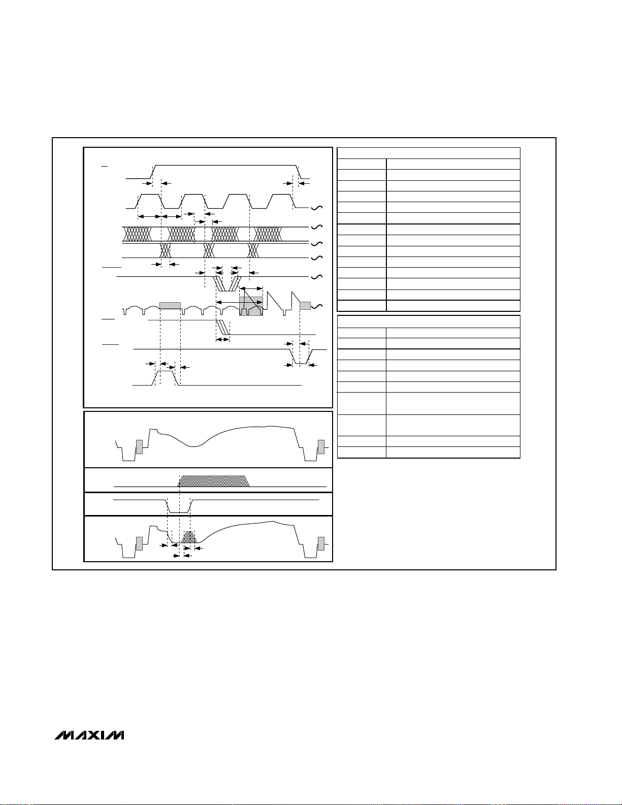
Figure 1. Timing Diagram
Ce: CE
Ck: SCLK
Di: DIN
Do: DOUT
Ud: UPDATE
Vo: OUT_
Ao: AOUT
Rst: RESET
t
PdHOeVo
Oe: OUTPUT ENABLE
IN_
t
PdDo
t
t
SuCe
MnHCk
t
MnLCk
Hi-Z
OSD: KEY AND FILL TIMING
DATA AND CONTROL TIMING
t
SuDi
t
HdDi
t
t
PdLOeVo
MnLUd
t
t
PdUdAo
PdUdVo
t
WTrVo
t
HdUd
VIDEO SOURCE
(SELECTED INPUT)
t
SuUd
t
HdCe
t
PdRstVo
t
MnlRst
Hi-Z
TIMING PARAMETER DEFINITIONS
NAME DESCRIPTION
t
HdDi
t
MnHCk
t
MnLCk
t
MnLUd
t
SuHUd
Hold Time: Clock to Data In
Min High Time: Clk
Min Low Time: Clk
Min Low Time: Update
Setup Time: UPDATE to Clk with UPDATE High
Not Valid Setup Time: UPDATE to Clk with UPDATE Low
t
HdHUd
Hold Time: Clk to UPDATE with UPDATE high
Not Valid Hold Time: Clk to UPDATE with UPDATE Low
t
PdDiDo
t
MnMd
t
MxTr
t
MnLRst
t
PdRstVo
Asynchronous Delay: Data In to Data Out
Min Low Time: MODE
Max Rise Time: Clk, Update
Min Low Time: Reset
Delay: Reset to Video Output
TIMING PARAMETER DEFINITIONS
NAME DESCRIPTION
t
PdUdVo
t
PdUdAo
t
PdOkVo
t
PdOfVo
t
PdDo
t
PdHOeVo
Delay: Update to Video Out
Delay: UPDATE to Aout
Delay: OSD Key to Video Output
Delay: OSD Fill to Video Output
Delay: Clk to Data Out
Delay: Output Enable to Video Output
(High: Disable)
t
PdLOeVo
Delay: Output Enable to Video Output
(Low: Enable)
t
t
SuCe
SuDi
Setup: Clock Enable to Clock
Setup Time: Data In to Clock
Of: OSDFILL
Ok: OSDKEY
OUT
i
i
i
t
PdHOkVo
(WITH SUPERIMPOSED OSD)
t
PdLOkVo
t
PdLOfVo
VIDEO OUTPUT

MAX4356
16 x 16 Nonblocking Video Crosspoint Switch
with On-Screen Display Insertion and I/O Buffers
14 ______________________________________________________________________________________
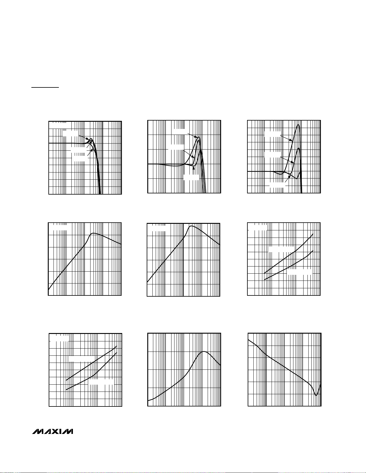
Typical Operating Characteristics—Dual Supplies ±5V
(VCC= +5V and VEE= -5V, VDD= +5V, AGND = DGND = 0, V
IN_
= 0, RL= 150Ω to AGND, and TA = +25°C, unless otherwise
noted.)
3
-7
0.1 1 10 100 1000
LARGE-SIGNAL FREQUENCY RESPONSE
-5
MAX4356 toc01
FREQUENCY (MHz)
NORMALIZED GAIN (dB)
-3
-1
1
0
-2
-4
-6
2
RL = 150Ω
AV = +2V/V
AV = +1V/V
3
-7
0.1 1 10 100 1000
MEDIUM-SIGNAL FREQUENCY RESPONSE
-5
MAX4356 toc02
FREQUENCY (MHz)
NORMALIZED GAIN (dB)
-3
-1
1
0
-2
-4
-6
2
RL = 150Ω
AV = +1V/V
AV = +2V/V
3
-7
0.1 1 10 100 1000
SMALL-SIGNAL FREQUENCY RESPONSE
-5
MAX4356 toc03
FREQUENCY (MHz)
NORMALIZED GAIN (dB)
-3
-1
1
0
-2
-4
-6
2
RL = 150Ω
AV = +1V/V
AV = +2V/V
3
-7
0.1 1 10 100 1000
LARGE-SIGNAL FREQUENCY RESPONSE
-5
MAX4356 toc04
FREQUENCY (MHz)
NORMALIZED GAIN (dB)
-3
-1
1
0
-2
-4
-6
2
RL = 1kΩ
AV = +1V/V
AV = +2V/V
3
-7
0.1 1 10 100 1000
MEDIUM-SIGNAL FREQUENCY RESPONSE
-5
MAX4356 toc05
FREQUENCY (MHz)
NORMALIZED GAIN (dB)
-3
-1
1
0
-2
-4
-6
2
RL = 1kΩ
AV = +2V/V
AV = +1V/V
3
-7
0.1 1 10 100 1000
SMALL-SIGNAL FREQUENCY RESPONSE
-5
MAX4356 toc06
FREQUENCY (MHz)
NORMALIZED GAIN (dB)
-3
-1
1
0
-2
-4
-6
2
RL = 1kΩ
AV = +1V/V
AV = +2V/V
0.3
-0.7
0.1 1 10 100 1000
LARGE-SIGNAL GAIN FLATNESS
vs. FREQUENCY
-0.5
MAX4356 toc07
FREQUENCY (MHz)
NORMALIZED GAIN (dB)
-0.3
-0.1
0.1
0
-0.2
-0.4
-0.6
0.2
AV = +1V/V
AV = +2V/V
RL = 150Ω
0.3
-0.7
0.1 1 10 100 1000
LARGE-SIGNAL GAIN FLATNESS
vs. FREQUENCY
-0.5
MAX4356 toc08
FREQUENCY (MHz)
NORMALIZED GAIN (dB)
-0.3
-0.1
0.1
0
-0.2
-0.4
-0.6
0.2
AV = +1V/V
AV = +2V/V
RL = 1kΩ
3
-7
0.1 1 10 100 1000
LARGE-SIGNAL FREQUENCY RESPONSE
(A
V
= +1V/V)
-5
MAX4356 toc09
FREQUENCY (MHz)
NORMALIZED GAIN (dB)
-3
-1
1
0
-2
-4
-6
2
RL = 150Ω
CL = 30pF
CL = 15pF
CL = 45pF
MAX4356
16 x 16 Nonblocking Video Crosspoint Switch
with On-Screen Display Insertion and I/O Buffers
______________________________________________________________________________________ 15
Typical Operating Characteristics—Dual Supplies ±5V (continued)
(VCC= +5V and VEE= -5V, VDD= +5V, AGND = DGND = 0, V
IN_
= 0, RL= 150Ω to AGND, and TA = +25°C, unless otherwise
noted.)
3
-7
0.1 1 10 100 1000
LARGE-SIGNAL FREQUENCY RESPONSE
(A
V
= +2V/V)
-5
MAX4356 toc10
FREQUENCY (MHz)
NORMALIZED GAIN (dB)
-3
-1
1
0
-2
-4
-6
2
RL = 150Ω
CL = 30pF
CL = 15pF
CL = 45pF
0.1 101 100 1000
MEDIUM-SIGNAL FREQUENCY RESPONSE
(A
V
= +1V/V)
MAX4356 toc11
FREQUENCY (MHz)
NORMALIZED GAIN (dB)
-10
-5
5
0
10
15
CL = 45pF
CL = 15pF
CL = 30pF
7
3
0.1 1 10 100 1000
MEDIUM-SIGNAL FREQUENCY RESPONSE
(A
V
= +2V/V)
1
MAX4356 toc12
FREQUENCY (MHz)
NORMALIZED GAIN (dB)
1
3
5
4
2
0
2
6
CL = 15pF
CL = 45pF
CL = 30pF
-40
-100
0.1 10 1001 1000
MAX4356 toc13
FREQUENCY (MHz)
CROSSTALK (dB)
-90
-80
-70
-60
-50
CROSSTALK vs. FREQUENCY
AV = +1V/V
-40
-100
0.1 10 1001 1000
MAX4356 toc14
FREQUENCY (MHz)
CROSSTALK (dB)
-90
-80
-70
-60
-50
CROSSTALK vs. FREQUENCY
AV = +2V/V
-10
-100
0.1 100101
DISTORTION vs. FREQUENCY
-70
-90
-30
-50
0
-60
-80
-20
-40
MAX4356 toc15
FREQUENCY (MHz)
DISTORTION ( dBc)
AV = +1V/V
2ND HARMONIC
3RD HARMONIC
-10
-100
0.1 100101
DISTORTION vs. FREQUENCY
-70
-90
-30
-50
0
-60
-80
-20
-40
MAX4356 toc16
FREQUENCY (MHz)
DISTORTION ( dBc)
AV = +2V/V
2ND HARMONIC
3RD HARMONIC
0.1 101 100 1000
ENABLED-OUTPUT IMPEDANCE
vs. FREQUENCY
MAX4356 toc17
FREQUENCY (MHz)
OUTPUT IMPEDIANCE (Ω)
1000
-0.1
1
10
100
1M
1
100k 10M 100M1M 1G
MAX4356 toc18
FREQUENCY (Hz)
OUTPUT IMPEDIANCE (Ω)
10
100
1k
10k
100k
DISABLED-OUTPUT IMPEDANCE
vs. FREQUENCY

MAX4356
16 x 16 Nonblocking Video Crosspoint Switch
with On-Screen Display Insertion and I/O Buffers
16 ______________________________________________________________________________________
Typical Operating Characteristics—Dual Supplies ±5V (continued)
(VCC= +5V and VEE= -5V, VDD= +5V, AGND = DGND = 0, V
IN_
= 0, RL= 150Ω to AGND, and TA = +25°C, unless otherwise
noted.)
-40
-50
-60
-70
-80
-90
-100
-110
-120
100k 10M 100M1M 1G
MAX4356 toc19
FREQUENCY (Hz)
OFF ISOLATION (dB)
OFF ISOLATION vs. FREQUENCY
10k 1M100k 10M 100M
POWER-SUPPLY REJECTION RATIO
vs. FREQUENCY
MAX4356 toc20
FREQUENCY (Hz)
PSRR (dB)
-75
-70
-60
-65
-55
-50
1000
1
10 10k 100k 1M100 1k 10M
INPUT VOLTAGE NOISE vs. FREQUENCY
100
MAX4356 toc21
FREQUENCY (Hz)
VOLTAGE NOISE (nV/√ Hz)
25ns/div
LARGE-SIGNAL PULSE RESPONSE
(A
V
= +1V/V)
INPUT
1V/div
OUTPUT
0.5V/div
MAX4356 toc22
25ns/div
LARGE-SIGNAL PULSE RESPONSE
(A
V
= +2V/V)
INPUT
0.5V/div
OUTPUT
0.5V/div
MAX4356 toc23
25ns/div
MEDIUM-SIGNAL PULSE RESPONSE
(A
V
= +1V/V)
INPUT
100mV/div
OUTPUT
50mV/div
MAX4356 toc24
25ns/div
MEDIUM-SIGNAL PULSE RESPONSE
(A
V
= +2V/V)
INPUT
50mV/div
OUTPUT
50mV/div
MAX4356 toc25
20ns/div
SWITCHING TIME
(A
V
= +1V/V)
V
UPDATE
5V/div
V
OUT
00mV/div
MAX4356 toc26
20ns/div
SWITCHING TIME
(A
V
= +2V/V)
V
UPDATE
5V/div
V
OUT
1V/div
MAX4356 toc27

MAX4356
16 x 16 Nonblocking Video Crosspoint Switch
with On-Screen Display Insertion and I/O Buffers
______________________________________________________________________________________ 17
Typical Operating Characteristics—Dual Supplies ±5V (continued)
(VCC= +5V and VEE= -5V, VDD= +5V, AGND = DGND = 0, V
IN_
= 0, RL= 150Ω to AGND, and TA = +25°C, unless otherwise
noted.)
20ns/div
SWITCHING TRANSIENT (GLITCH)
(A
V
= +1V/V)
V
UPDATE
5V/div
V
OUT
25mV/div
MAX4356 toc28
20ns/div
SWITCHING TRANSIENT (GLITCH)
(A
V
= +2V/V)
V
UPDATE
5V/div
V
OUT
25mV/div
MAX4356 toc29
0
100
50
200
150
250
300
-15
-11
-9 -7-13 -5 -3 -1
1
3
5
OFFSET VOLTAGE DISTRIBUTION
MAX4356 toc30
OFFSET VOLTAGE (mV)
-0.05
0102030405060708090100
0102030405060708090100
DIFFERENTIAL GAIN AND PHASE
(R
L
= 150Ω)
0.00
0.00
-0.02
0.05
0.02
0.04
0.10
006
0.08
0.15
IRE
DIFF PHASE (°)
DIFF GAIN (%)
MAX4356 toc31
0.01
0.00
0102030 405060708090100
0102030 405060708090100
DIFFERENTIAL GAIN AND PHASE
(R
L
= 1kΩ)
-0.004
0.02
-0.002
0.000
0.002
0.004
0.03
IRE
DIFF PHASE (°)
DIFF GAIN (%)
MAX4356 toc32
-0.01
25ns/div
LARGE-SIGNAL PULSE RESPONSE WITH
CAPACITIVE LOAD (C
L
= 30pF, AV = +1V/V)
INPUT
1V/div
OUTPUT
0.5/Vdiv
MAX4356 toc33
25ns/div
LARGE-SIGNAL PULSE RESPONSE WITH
CAPACITIVE LOAD (C
L
= 30pF, AV = +2V/V)
INPUT
0.5V/div
OUTPUT
0.5/Vdiv
MAX4356 toc34
25ns/div
MEDIUM-SIGNAL PULSE RESPONSE WITH
CAPACITIVE LOAD (C
L
= 30pF, AV = +1V/V)
INPUT
100mV/div
OUTPUT
50mV/div
MAX4356 toc35
25ns/div
MEDIUM-SIGNAL PULSE RESPONSE WITH
CAPACITIVE LOAD (C
L
= 30pF, AV = +2V/V)
INPUT
50mV/div
OUTPUT
50mV/div
MAX4356 toc36

MAX4356
16 x 16 Nonblocking Video Crosspoint Switch
with On-Screen Display Insertion and I/O Buffers
18 ______________________________________________________________________________________
Typical Operating Characteristics—Dual Supplies ±5V (continued)
(VCC= +5V and VEE= -5V, VDD= +5V, AGND = DGND = 0, V
IN_
= 0, RL= 150Ω to AGND, and TA = +25°C, unless otherwise
noted.)
-0.20
-0.15
-0.10
-0.05
0
0.05
0.10
0.15
0.20
-50 0-25 25 50 75 100
GAIN vs. TEMPERATURE
MAX4356 toc37
TEMPERATURE (°C)
NORMALIZED GAIN (dB)
AV = +2V/V
AV = +1V/V
1p 10n 1µ100p10p 1n 100n 10µ
100µ
MAX4356 toc38
10n
10µ
1µ
100n
100µ
1m
10m
100m
10
1
RESET DELAY vs. C
RESET
RESET DELAY (s)
C
RESET
(F)
OSD SWITCHING TRANSIENT
(100IRE LEVEL SWITCH) (A
V
= +2V/V)
MAX4356 toc39
50ns/div
V
OSDKEY0
5V/div
V
OUT0
500mV/div
100IRE
0IRE
OSD SWITCHING 3.58MHz SIGNAL
(A
V
= +2V/V)
MAX4356 toc40
50ns/div
V
OSDKEY0
5V/div
V
OUT0
500mV/div
0
20
10
40
30
60
50
70
-50 0 25-25 50 75 100
SUPPLY CURRENT vs. TEMPERATURE
MAX4358 toc41
TEMPERATURE (°C)
SUPPLY CURRENT (mA)
I
CC
I
EE
I
DD

MAX4356
16 x 16 Nonblocking Video Crosspoint Switch
with On-Screen Display Insertion and I/O Buffers
______________________________________________________________________________________ 19
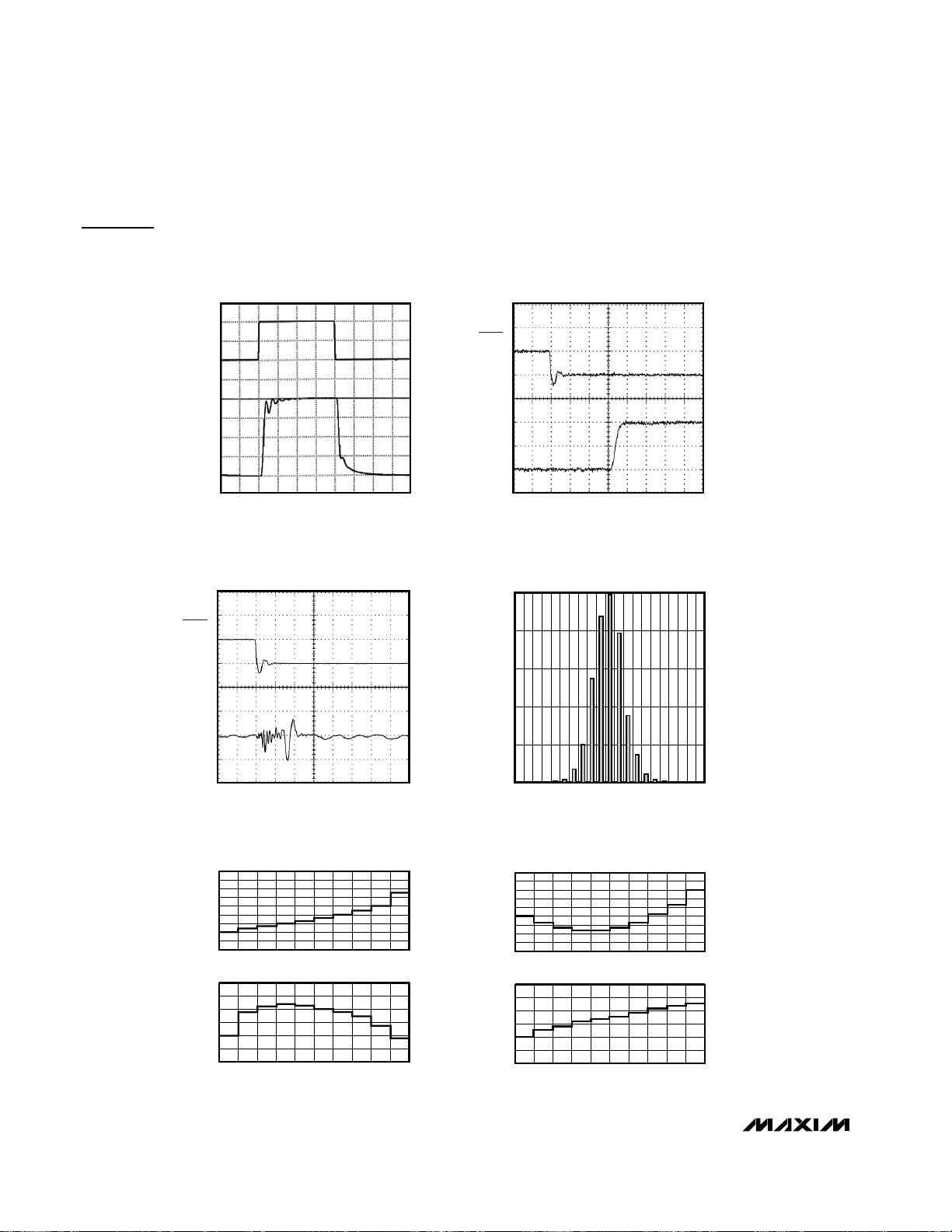
Typical Operating Characteristics—Dual Supplies ±3V
(VCC= +3V and VEE= -3V, VDD= +3V, AGND = DGND = 0, V
IN_
= 0, RL= 150Ω to AGND, and TA = +25°C, unless otherwise
noted.)
3
-7
0.1 1 10 100 1000
LARGE-SIGNAL FREQUENCY
RESPONSE
-5
MAX4356 toc42
FREQUENCY (MHz)
NORMALIZED GAIN (dB)
-3
-1
1
0
-2
-4
-6
2
RL = 150Ω
AV = +1V/V
AV = +2V/V
3
-7
0.1 1 10 100 1000
MEDIUM-SIGNAL FREQUENCY
RESPONSE
-5
MAX4356 toc43
FREQUENCY (MHz)
NORMALIZED GAIN (dB)
-3
-1
1
0
-2
-4
-6
2
RL = 150Ω
AV = +1V/V
Av = +2V/V
3
-7
0.1 1 10 100 1000
SMALL-SIGNAL FREQUENCY
RESPONSE
-5
MAX4356 toc44
FREQUENCY (MHz)
NORMALIZED GAIN (dB)
-3
-1
1
0
-2
-4
-6
2
RL = 150Ω
AV = +1V/V
AV = +2V/V
3
-7
0.1 1 10 100 1000
LARGE-SIGNAL FREQUENCY
RESPONSE
-5
MAX4356 toc45
FREQUENCY (MHz)
NORMALIZED GAIN (dB)
-3
-1
1
0
-2
-4
-6
2
RL = 1kΩ
AV = +2V/V
AV = +1V/V
3
-7
0.1 1 10 100 1000
MEDIUM-SIGNAL FREQUENCY
RESPONSE
-5
MAX4356 toc46
FREQUENCY (MHz)
NORMALIZED GAIN (dB)
-3
-1
1
0
-2
-4
-6
2
RL = 1kΩ
AV = +1V/V
AV = +2V/V
3
-7
0.1 1 10 100 1000
SMALL-SIGNAL FREQUENCY
RESPONSE
-5
MAX4356 toc47
FREQUENCY (MHz)
NORMALIZED GAIN (dB)
-3
-1
1
0
-2
-4
-6
2
RL = 1kΩ
AV = +1V/V
AV = +2V/V
0.3
-0.7
0.1 1 10 100 1000
LARGE-SIGNAL GAIN FLATNESS
-0.5
MAX4356 toc48
FREQUENCY (MHz)
NORMALIZED GAIN (dB)
-0.3
-0.1
0.1
0
-0.2
-0.4
-0.6
0.2
RL = 150Ω
AV = +1V/V
AV = +2V/V
0.3
-0.7
0.1 1 10 100 1000
LARGE-SIGNAL GAIN FLATNESS
-0.5
MAX4356 toc49
FREQUENCY (MHz)
NORMALIZED GAIN (dB)
-0.3
-0.1
0.1
0
-0.2
-0.4
-0.6
0.2
RL = 1kΩ
AV = +1V/V
AV = +2V/V
3
-7
0.1 1 10 100 1000
LARGE-SIGNAL FREQUENCY RESPONSE
(A
V
= +1V/V)
-5
MAX4356 toc50
FREQUENCY (MHz)
NORMALIZED GAIN (dB)
-3
-1
1
0
-2
-4
-6
2
CL = 15pF
CL = 45pF
CL = 30pF

MAX4356
16 x 16 Nonblocking Video Crosspoint Switch
with On-Screen Display Insertion and I/O Buffers
20 ______________________________________________________________________________________
Typical Operating Characteristics—Dual Supplies ±3V (continued)
(VCC= +3V and VEE= -3V, VDD= +3V, AGND = DGND = 0, V
IN_
= 0, RL= 150Ω to AGND, and TA = +25°C, unless otherwise
noted.)
3
-7
0.1 1 10 100 1000
LARGE-SIGNAL FREQUENCY RESPONSE
(A
V
= +2V/V)
-5
MAX4356 toc51
FREQUENCY (MHz)
NORMALIZED GAIN (dB)
-3
-1
1
0
-2
-4
-6
2
CL = 15pF
CL = 45pF
CL = 30pF
8
-8
0.1 1 10 100 1000
MEDIUM-SIGNAL FREQUENCY RESPONSE
(A
V
= +1V/V)
MAX4356 toc52
FREQUENCY (MHz)
NORMALIZED GAIN (dB)
-2
2
4
0
-4
-6
6
CL = 30pF
CL = 45pF
CL = 15pF
6
-4
0.1 1 10 100 1000
MEDIUM-SIGNAL FREQUENCY RESPONSE
(A
V
= +2V/V)
-2
MAX4356 toc53
FREQUENCY (MHz)
NORMALIZED GAIN (dB)
0
2
4
3
1
-1
-3
5
CL = 45pF
CL = 30pF
CL = 15pF
-40
-90
1k 1M 10M 100M 1G
CROSSTALK VS. FREQUENCY
-80
MAX4356 toc54
FREQUENCY (Hz)
CROSSTALK (dB)
-70
-60
-50
-55
-65
-75
-85
-45
AV = +1V/V
-30
-80
0.1 1 10 100 1000
CROSSTALK VS. FREQUENCY
-70
MAX4356 toc55
FREQUENCY (MHz)
CROSSTALK (dB)
-60
-50
-40
-45
-55
-65
-75
-35
AV = + 2V/V
-10
-100
0.1 100101
DISTORTION VS. FREQUENCY
-70
-90
-30
-50
0
-60
-80
-20
-40
MAX4356 toc56
FREQUENCY (MHz)
DISTORTION (dBc)
AV = + 1V/V
2ND HARMONIC
3RD HARMONIC
-10
-100
0.1 100M10M1M
DISTORTION VS. FREQUENCY
-70
-90
-30
-50
0
-60
-80
-20
-40
MAX4356 toc57
FREQUENCY (Hz)
CROSSTALK (dBc)
AV = +2 V/V
2ND HARMONIC
3RD HARMONIC
0.1 101 100 1000
ENABLED OUTPUT IMPEDANCE
VS. FREQUENCY
MAX4356 toc58
FREQUENCY (MHz)
OUTPUT IMPEDANCE (Ω)
1000
0.1
1
10
100
1M
1
0.1 10 1001 1000
DISABLED OUTPUT IMPEDANCE
VS. FREQUENCY
MAX4356 toc59
FREQUENCY (MHz)
OUTPUT IMPEDANCE (Ω)
10
100
1k
10k
100k

MAX4356
16 x 16 Nonblocking Video Crosspoint Switch
with On-Screen Display Insertion and I/O Buffers
______________________________________________________________________________________ 21
Typical Operating Characteristics—Dual Supplies ±3V (continued)
(VCC= +3V and VEE= -3V, VDD= +3V, AGND = DGND = 0, V
IN_
= 0, RL= 150Ω to AGND, and TA = +25°C, unless otherwise
noted.)
-40
-50
-60
-70
-80
-90
-100
-110
-120
100k 10M 100M1M 1G
OFF ISOLATION VS. FREQUENCY
MAX4356 toc60
FREQUENCY (Hz)
OFF ISOLATION (dB)
-50
-75
10k 100k 10M 100M
POWER-SUPPLY REJECTION RATIO
VS. FREQUENCY
-70
-65
-55
MAX4356 toc61
FREQUENCY (Hz)
PSRR (dB)
1M
1000
10
10 10k 100k 1M100 1k 10M
INPUT VOLTAGE NOISE
vs. FREQUENCY
100
MAX4356 toc62
FREQUENCY (Hz)
VOLTAGE NOISE (nV/ Hz)
LARGE-SIGNAL PULSE RESPONSE
(A
V
= +1V/V)
MAX4356 toc63
OUTPUT
0.5V/div
INPUT
1V/div
25ns/div
LARGE-SIGNAL PULSE RESPONSE
(A
V
= +2V/V)
MAX4356 toc64
OUTPUT
0.5V/div
INPUT
0.5V/div
25ns/div
MEDIUM-SIGNAL PULSE RESPONSE
(A
V
= +1V/V)
MAX4356 toc65
OUTPUT
50mV/div
INPUT
100mV/div
25ns/div
MEDIUM-SIGNAL PULSE RESPONSE
(A
V
= +2V/V)
MAX4356 toc66
OUTPUT
50mV/div
INPUT
50mV/div
25ns/div
SWITCHING TIME
(A
V
= +1V/V)
MAX4356 toc67
V
OUT
V
UPDATE
3V/div
20ns/div
SWITCHING TIME
(A
V
= +2V/V)
MAX4356 toc68
V
OUT
1V/div
V
UPDATE
3V/div
20ns/div

MAX4356
16 x 16 Nonblocking Video Crosspoint Switch
with On-Screen Display Insertion and I/O Buffers
22 ______________________________________________________________________________________
Typical Operating Characteristics—Dual Supplies ±3V (continued)
(VCC= +3V and VEE= -3V, VDD= +3V, AGND = DGND = 0, V
IN_
= 0, RL= 150Ω to AGND, and TA = +25°C, unless otherwise
noted.)
SWITCHING TRANSIENT (GLITCH)
MAX4356 toc69
(AV = +1V/V)
V
OUT
25mV/div
V
UPDATE
3V/div
20ns/div
SWITCHING TRANSIENT (GLITCH)
MAX4356 toc70
(AV = +2V/V)
V
OUT
25mV/div
V
UPDATE
3V/div
20ns/div
50
0
150
100
250
200
300
-15 -11 -9 -7-13 -5 -3 -1 1 3 5
OFFSET VOLTAGE DISTRIBUTION
MAX4356 toc71
OFFSET VOLTAGE (mV)
0.05
0
-0.05
0.15
0.10
0.20
0.05
0
-0.05
0.15
0.10
0.20
0.25
10 30 40 5020 60 70 80 90 100
DIFFERENTIAL GAIN AND PHASE
(R
L
= 150Ω)
MAX4356 toc72
IRE
DIFFERENTIAL
GAIN (%)
DIFFERENTIAL
PHASE (°)
0.02
0
-0.02
0.06
0.04
0.08
10 30 40 5020 60 70 80 90 100
DIFFERENTIAL GAIN AND PHASE
(R
L
= 1kΩ)
MAX4356 toc73
IRE
DIFFERENTIAL
GAIN (%)
DIFFERENTIAL
PHASE (°)
0.015
0.020
0
0.010
0.005
0.010
LARGE-SIGNAL PULSE RESPONSE
WITH CAPACITIVE LOAD
(C
L
= 30pF, AV = +1V/V)
MAX4356 toc74
OUTPUT
500mV/div
INPUT
1V/div
25ns/div
LARGE-SIGNAL PULSE RESPONSE
WITH CAPACITIVE LOAD
(C
L
= 30pF, AV = + 2V/V)
MAX4356 toc75
OUTPUT
0.5V/div
INPUT
0.5V/div
25ns/div
MEDIUM-SIGNAL PULSE RESPONSE
WITH CAPACITIVE LOAD
(C
L
= 30pF, AV = + 1V/V)
MAX4356 toc76
OUTPUT
50mV/div
100mV/div
25ns/div
MEDIUM-SIGNAL PULSE RESPONSE
WITH CAPACITIVE LOAD
(C
L
= 30pF, AV = + 2V/V)
MAX4356 toc77
OUTPUT
50mV/div
INPUT
50mV/div
25ns/div

MAX4356
16 x 16 Nonblocking Video Crosspoint Switch
with On-Screen Display Insertion and I/O Buffers
______________________________________________________________________________________ 23
Typical Operating Characteristics—Dual Supplies ±3V (continued)
(VCC= +3V and VEE= -3V, VDD= +3V, AGND = DGND = 0, V
IN_
= 0, RL= 150Ω to AGND, and TA = +25°C, unless otherwise
noted.)
-50 0-25 25 50 75 100
GAIN VS. TEMPERATURE
MAX4356 toc78
TEMPERATURE (°C)
NORMALIZED GAIN (dB)
-0.20
-0.15
-0.05
-0.10
0.10
0.15
0.05
0.20
0
AV = +2V/V
AV = +1V/V
1p 10n 1
µ100p10p 1n 100n 10µ
100µ
MAX4356 toc79
10n
10µ
1µ
100n
100µ
1m
10m
100m
10
1
RESET DELAY vs. C
RESET
RESET DELAY (s)
C
RESET
(F)
OSD SWITCHING TRANSIENT
(100IRE LEVEL SWITCH)
MAX4356 toc80
V
OUT0
500mV/div
V
OSDKEY0
3V/div
50ns/div
100IRE
0IRE
AV = +2V/V
OSD SWITCHING 3.58MHz SIGNAL
MAX4356 toc81
V
OUT0
500mV/div
V
OSDKEY0
3V/div
50ns/div
AV = + 2V/V

3
-7
100k 1M 10M 100M 1G
LARGE-SIGNAL FREQUENCY RESPONSE
-5
MAX4356 toc85
FREQUENCY (Hz)
NORMALIZED GAIN (dB)
-3
-1
1
0
-2
-4
-6
2
RL = 1kΩ
MAX4356
16 x 16 Nonblocking Video Crosspoint Switch
with On-Screen Display Insertion and I/O Buffers
24 ______________________________________________________________________________________
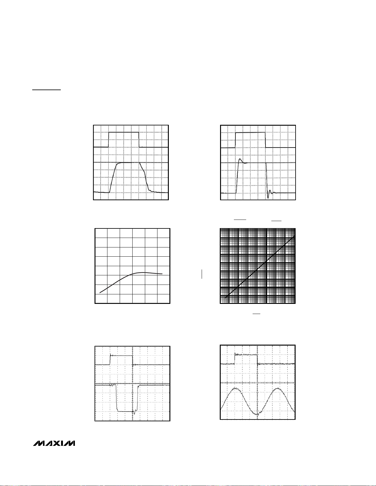
Typical Operating Characteristics—Single Supply +5V
(VCC= +5V and VEE= 0, VDD= +5V, AGND = DGND = 0, V
IN_
= 0, RL= 150Ω to AGND, AV= +1V/V, and TA = +25°C, unless oth-
erwise noted.)
3
-7
0.1 1 10 100 1000
LARGE-SIGNAL FREQUENCY RESPONSE
-5
MAX4356 toc82
FREQUENCY (MHz)
NORMALIZED GAIN (dB)
-3
-1
1
0
-2
-4
-6
2
RL = 150Ω
3
-7
0.1 1 10 100 1000
MEDIUM-SIGNAL FREQUENCY RESPONSE
-5
MAX4356 toc83
FREQUENCY (MHz)
NORMALIZED GAIN (dB)
-3
-1
1
0
-2
-4
-6
2
RL = 150Ω
3
-7
0.1 1 10 100 1000
SMALL-SIGNAL FREQUENCY RESPONSE
-5
MAX4356 toc84
FREQUENCY (MHz)
NORMALIZED GAIN (dB)
-3
-1
1
0
-2
-4
-6
2
RL = 150Ω
3
-7
100k 1M 10M 100M 1G
MEDIUM-SIGNAL FREQUENCY RESPONSE
-5
MAX4356 toc86
FREQUENCY (Hz)
NORMALIZED GAIN (dB)
-3
-1
1
0
-2
-4
-6
2
RL = 1kΩ
3
-7
100k 1M 10M 100M 1G
SMALL-SIGNAL FREQUENCY RESPONSE
-5
MAX4356 toc87
FREQUENCY (Hz)
NORMALIZED GAIN (dB)
-3
-1
1
0
-2
-4
-6
2
RL = 1kΩ
0.3
-0.7
0.1 1 10 100 1000
LARGE-SIGNAL GAIN FLATNESS
-0.5
MAX4356 toc88
FREQUENCY (MHz)
NORMALIZED GAIN (dB)
-0.3
-0.1
0.1
0
-0.2
-0.4
-0.6
0.2
RL = 150Ω
0.3
-0.7
0.1 1 10 100 1000
LARGE-SIGNAL GAIN FLATNESS
-0.5
MAX4356 toc89
FREQUENCY (MHz)
NORMALIZED GAIN (dB)
-0.3
-0.1
0.1
0
-0.2
-0.4
-0.6
0.2
RL = 1kΩ
3
-7
0.1 1 10 100 1000
LARGE-SIGNAL FREQUENCY RESPONSE
-5
MAX4356 toc90
FREQUENCY (MHz)
NORMALIZED GAIN (dB)
-3
-1
1
0
-2
-4
-6
2
CL = 15pF
CL = 45pF
CL = 30pF

MAX4356
16 x 16 Nonblocking Video Crosspoint Switch
with On-Screen Display Insertion and I/O Buffers
______________________________________________________________________________________ 25
Typical Operating Characteristics—Single Supply +5V (continued)
(VCC= +5V and VEE= 0, VDD= +5V, AGND = DGND = 0, V
IN_
= 0, RL= 150Ω to AGND, AV= +1V/V, and TA = +25°C, unless oth-
erwise noted.)
7
-7
100k 1M 10M 100M 1G
MEDIUM-SIGNAL FREQUENCY RESPONSE
MAX4356 toc91
FREQUENCY (Hz)
NORMALIZED GAIN (dB)
-1
1
3
-3
-5
5
CL = 15pF
CL = 45pF
CL = 30pF
-50
-100
100k 1M 10M 100M 1G
CROSSTALK vs. FREQUENCY
-90
MAX4356 toc92
FREQUENCY (MHz)
CROSSTALK (dB)
-80
-70
-60
-65
-75
-85
-95
-55
0
-100
0.1 1 10 100
DISTORTION vs. FREQUENCY
-80
MAX4356 toc93
FREQUENCY (MHz)
DISTORTION (Ω)
-60
-40
-20
-30
-50
-70
-90
-10
2ND HARMONIC
3RD HARMONIC
0.1 101 100 1000
ENABLED-OUTPUT IMPEDANCE
vs. FREQUENCY
MAX4356 toc94
FREQUENCY (MHz)
OUTPUT IMPEDANCE (Ω)
1k
0.1
1
10
100
1M
1
100k 10M 100M1M 1G
MAX4356 toc95
FREQUENCY (Hz)
OUTPUT IMPEDANCE (Ω)
10
100
1k
10k
100k
DISABLED-OUTPUT IMPEDANCE
vs. FREQUENCY
-40
-50
-60
-70
-80
-90
-100
-110
-120
100k 10M 100M1M 1G
MAX4356 toc96
FREQUENCY (Hz)
OFF ISOLATION (dB)
OFF ISOLATION vs. FREQUENCY
10k 1M100k 10M 100M
POWER-SUPPLY REJECTION RATIO
vs. FREQUENCY
MAX4356 toc97
FREQUENCY (Hz)
PSRR (dB)
-75
-70
-60
-65
-55
-50
1000
1
10 10k 100k 1M100 1k 10M
INPUT VOLTAGE NOISE vs. FREQUENCY
100
MAX4356 toc98
FREQUENCY (Hz)
VOLTAGE NOISE (nV/√ Hz)
LARGE-SIGNAL PULSE RESPONSE
MAX4356 toc99
25ns/div
INPUT
1V/div
OUTPUT
0.5V/div
MAX4356
16 x 16 Nonblocking Video Crosspoint Switch
with On-Screen Display Insertion and I/O Buffers
26 ______________________________________________________________________________________
Typical Operating Characteristics—Single Supply +5V (continued)
(VCC= +5V and VEE= 0, VDD= +5V, AGND = DGND = 0, V
IN_
= 0, RL= 150Ω to AGND, AV= +1V/V, and TA = +25°C, unless oth-
erwise noted.)
MEDIUM-SIGNAL PULSE RESPONSE
MAX4356 toc100
25ns/div
INPUT
100mV/div
OUTPUT
50mV/div
SWITCHING TIME
MAX4356 toc101
20ns/div
V
UPDATE
5V/div
V
OUT
500mV/div
SWITCHING TRANSIENT (GLITCH)
MAX4356 toc102
20ns/div
V
UPDATE
5V/div
V
OUT
25mV/div
0
50
150
100
200
250
-20 -16 -14 -12-18 -10 -8 -6 -4 -2 0
OFFSET VOLTAGE HISTOGRAM
MAX4356 toc103
OFFSET VOLTAGE (mV)
-0.1
0102030 405060708090100
0102030 405060708090100
DIFFERENTIAL GAIN AND PHASE
(R
L
= 150Ω)
0.0
0.20
0.10
0.00
-0.10
0.1
0.2
0.30
0.3
IRE
DIFF PHASE (°)
DIFF GAIN (%)
MAX4356 toc104
-0.02
0102030 405060708090100
0102030 405060708090100
DIFFERENTIAL GAIN AND PHASE
(R
L
= 1kΩ)
0.00
0.10
0.00
0.10
-0.20
0.02
0.04
0.20
0.06
IRE
DIFF PHASE (°)
DIFF GAIN (%)
MAX4356 toc105
MAX4356
16 x 16 Nonblocking Video Crosspoint Switch
with On-Screen Display Insertion and I/O Buffers
______________________________________________________________________________________ 27
Typical Operating Characteristics—Single Supply +5V (continued)
(VCC= +5V and VEE= 0, VDD= +5V, AGND = DGND = 0, V
IN_
= 0, RL= 150Ω to AGND, AV= +1V/V, and TA = +25°C, unless oth-
erwise noted.)
LARGE-SIGNAL PULSE RESPONSE WITH
CAPACITIVE LOAD (C
L
= 30pF)
MAX4356 toc106
25ns/div
INPUT
1V/div
OUTPUT
0.5V/div
MEDIUM-SIGNAL PULSE RESPONSE WITH
CAPACITIVE LOAD (C
L
= 30pF)
MAX4356 toc107
25ns/div
INPUT
100mV/div
OUTPUT
50mV/div
-0.20
-0.15
-0.10
-0.05
0
0.05
0.10
0.15
0.20
-50 0-25 25 50 75 100
GAIN vs. TEMPERATURE
MAX4356 toc108
TEMPERATURE (°C)
NORMALIZED GAIN (dB)
1p 10n 1
µ100p10p 1n 100n 10µ
100µ
MAX4356 toc109
10n
10µ
1µ
100n
100µ
1m
10m
100m
10
1
RESET DELAY vs. C
RESET
RESET DELAY (s)
C
RESET
(F)
OSD SWITCHING TRANSIENT
(100IRE LEVEL SWITCH)
MAX4356 toc110
50ns/div
V
OSDKEY0
5V/div
V
OUT0
250mV/div
100IRE
0IRE
50ns/div
OSD SWITCHING 3.58MHz SIGNAL
V
OSDKEY0
5V/div
V
OUT0
250mV/div
MAX4356 toc111

MAX4356
16 x 16 Nonblocking Video Crosspoint Switch
with On-Screen Display Insertion and I/O Buffers
28 ______________________________________________________________________________________
Pin Description
PIN NAME FUNCTION
1–4, 30–38, 103 N.C. No Connection. Not internally connected. Connect to AGND.
5, 7, 9, 11, 13,
15, 17, 19, 21, 23,
25, 27, 121, 123,
125, 127
6, 8, 10, 12, 14,
16, 18, 20, 65, 66,
100, 101, 102,
120, 122, 124,
126
22, 24, 26, 28 A3–A0
29, 67, 71, 75, 79,
83, 87, 91, 95, 99
39 DOUT
40 DGND Digital Ground
41 AOUT Address Recognition Output. AOUT drives low after successful chip address recognition.
42 SCLK Serial Clock Input
43 CE Clock Enable Input. Drive low to enable the serial data interface.
44 MODE
45 RESET
46 UPDATE Update Input. Drive UPDATE low to transfer data from Mode registers to the matrix switch.
47 DIN Serial Data Input. Data is clocked in on the falling edge of SCLK.
48 V
IN0–IN15 Buffered Analog Inputs
AGND Analog Ground
Address Programming Inputs. Connect to DGND or V
output address mode. See Table 3.
V
CC
DD
Positive Analog Supply. Bypass each pin with a 0.1µF capacitor to AGND. Connect a single
10µF capacitor from one V
Serial Data Output. In complete matrix mode, data is clocked through the 96-bit Matrix Control
Shift register. In individual output address mode, data at DIN passes directly to DOUT.
Serial Interface Mode Select Input. Drive high for complete matrix mode (mode 1), or drive low
for individual output address mode (mode 0).
Asynchronous Reset Input/Output. Drive RESET low to initiate hardware reset. All matrix
settings are set to power-up defaults and all analog outputs are disabled. Additional power-on
reset delay may be set by connecting a small capacitor from RESET to DGND.
Digital Logic Supply. Bypass VDD with a 0.1µF capacitor DGND.
pin to AGND.
CC
to select the address for individual
DD
49–64
68, 70, 72, 74, 76,
78, 80, 82, 84, 86,
88, 90, 92, 94, 96,
98
69, 73, 77, 81, 85,
89, 93, 97, 128
104–119
OSDKEY0–
OSDKEY15
OUT0–
OUT15
V
EE
OSDFILL0–
OSDFILL15
Digital Control Input. Control for the fast 2:1 OSD insertion multiplexer routing signal to output
buffers. A logic high routes the programmed IN_ analog input signal to the output buffer. A
logic low routes the dedicated OSDFILL_ input to the corresponding output buffer.
Buffered Analog Outputs. Gain is individually programmable for A
through the serial interface. Outputs may be individually disabled (high impedance). On
power-up or assertion of RESET, all outputs are disabled.
Negative Analog Supply. Bypass each pin with a 0.1µF capacitor to AGND. Connect a single
10µF capacitor from one V
Dedicated OSD Analog Signal Buffered Inputs. For each output buffer amplifier OSDFILL, the
input signal is routed to output buffer amplifier OUT when the corresponding OSDKEY is low.
pin to AGND.
EE
= +1V/V or AV = +2V/V
V
MAX4356
16 x 16 Nonblocking Video Crosspoint Switch
with On-Screen Display Insertion and I/O Buffers
______________________________________________________________________________________ 29
Detailed Description
The MAX4356 is a highly integrated 16 ✕16 nonblocking video crosspoint switch matrix. All inputs and outputs are buffered, with all outputs able to drive
standard 75Ω reverse-terminated video loads.
A 3-wire interface programs the switch matrix and initializes with a single update signal. The unique serial
interface operates in one of two modes: Complete
Matrix Mode (Mode 1) or Individual Output Address
Mode (Mode 0).
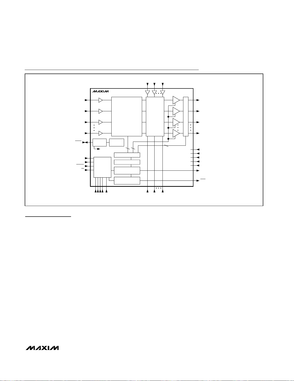
In the Functional Diagram, the signal path of the
MAX4356 is from the inputs (IN0–IN15), through the
switching matrix, buffered by the output amplifiers, and
presented at the output terminals (OUT0–OUT15). The
other functional blocks are the serial interface and control logic. Each of the functional blocks is described in
detail below.
Analog Outputs
The MAX4356 outputs are high-speed voltage feedback amplifiers capable of driving 150Ω (75Ω back-terminated) loads. The gain, AV= +1V/V or +2V/V, is
selectable through programming bit 4 of the serial control word. Amplifier compensation is automatically opti-
mized to maximize the bandwidth for each gain selection. Each output can be individually enabled and disabled through bit 5 of the serial control word. When
disabled, the output is high impedance, presenting typically a 4kΩ load, and 3pF output capacitance, allowing
multiple outputs to be connected together in building
large arrays. On power-up (or asynchronous RESET),
all outputs are initialized in the disabled state to avoid
output conflicts in large array configurations. The programming and operation of the MAX4356 is output
referred. Outputs are configured individually to connect
to any one of the 16 analog inputs, programmed to the
desired gain (AV= +1V/V or +2V/V), or disabled in a
high-impedance state.
Analog Inputs
The MAX4356 offers 16 analog input channels. Each
input is buffered before the crosspoint switch matrix,
allowing one input to cross-connect to up to 16 outputs.
The input buffers are voltage feedback amplifiers with
high input impedance and low-input bias current. This
allows the use of very simple input clamp circuits.
Functional Diagram
RESET
UPDATE
IN0
IN1
IN2
IN15
DIN
SCLK
CE
MAX4356
POWER-ON
RESET
DISABLE ALL OUTPUTS
SERIAL
INTERFACE
A0-A3 MODE
*AV = +1V/V OR +2V/V
SWITCH MATRIX
THERMAL
SHUTDOWN
MATRIX REGISTER
UPDATE REGISTER
16 x 16
256
DECODE LOGIC
LATCHES
96 BITS
16 BITS
OSDFILL0 OSDFILL15
16
OSDKEY0 OSDKEY15
OSDFILL1
2:1
OSD
MUX
OSDKEY1
AV*
A
*
V
*
A
V
A
*
V
16
OUT0
OUT1
OUT2
ENABLE/DISABLE
OUT15
V
V
AGND
DGND
DOUT
AOUT
CC
EE
V
DD
MAX4356
16 x 16 Nonblocking Video Crosspoint Switch
with On-Screen Display Insertion and I/O Buffers
30 ______________________________________________________________________________________
OSDFILL and OSDKEY Inputs
Intended for on-screen display insertion, the 16 OSDFILL inputs are buffered analog signal inputs that are
routed exclusively to a dedicated output buffer through
a fast 2:1 Mux. The signal presented to the output
buffer is selected from the programmed analog input
signal (IN_) and the dedicated OSDFILL input signal.
Each OSD Insertion Mux is controlled through the corresponding OSDKEY digital input to provide fast pixel
switching.
Switch Matrix
The MAX4356 has 256 individual T-switches making a
16 x 16 switch matrix . The switching matrix is 100%
nonblocking, which means that any input may be routed to any output. The switch matrix programming is
output-referred. Each output may be connected to any
one of the 16 analog inputs. Any one input can be routed to all 16 outputs with no signal degradation.
Digital Interface
The digital interface consists of the following pins: DIN,
DOUT, SCLK, AOUT, UPDATE, CE, A3–A0, MODE, and
RESET. DIN is the serial data input; DOUT is the serial
data output. SCLK is the serial data clock that clocks
data into the Data Input registers (Figure 2). Data at
DIN is loaded at each falling edge of SCLK. DOUT is
the data shifted out of the 96-bit Complete Matrix Mode
(Mode = 1). DIN passes directly to DOUT when in
Individual Output Address Mode (Mode = 0).
The falling edge of UPDATE latches the data and programs the matrix. When using individual output
address mode, the address recognition output AOUT
drives low when control word bits D13 to D10 match
the address programming inputs (A3–A0) and UPDATE
is low. Table 1 is the operation truth table.
Programming the Matrix
The MAX4356 offers two programming modes: individual output address mode and complete matrix mode.
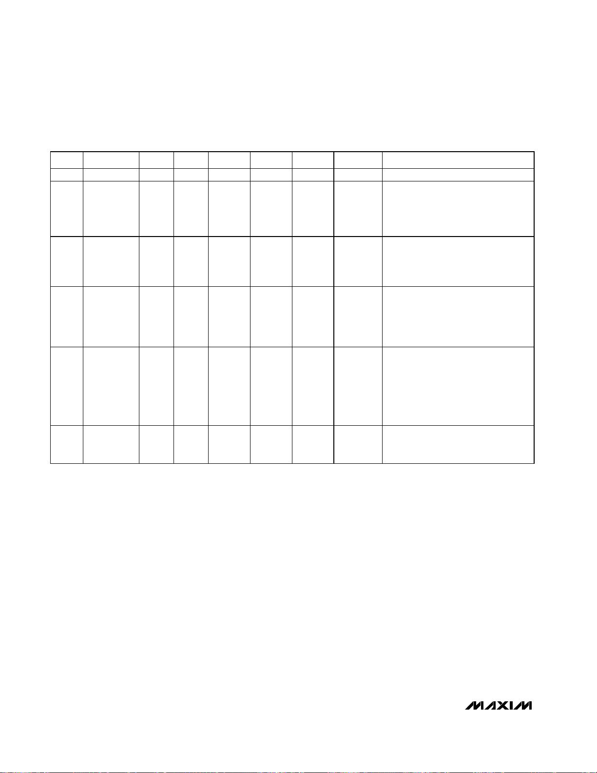
Table 1. Operation Truth Table
CE UPDATE SCLK DIN DOUT MODE AOUT RESET OPERATION/COMMENTS
1 X X X X X X 1 No change in logic.
Data at DIN is clocked on the negative
edge of the SCLK into the 96-bit
01↓ D
00XXX111
01↓ D
D
i
i
i-96
D
i
11 1
01 1
Complete Matrix Mode register. DOUT
supplies original data in 96 SCLK
pulses later.
Data in the serial 96-bit Complete
Matrix Mode register is transferred
into parallel latches that control the
switching matrix.
Data at DIN is routed to the Individual
Output Address Mode shift register.
DIN is also connected directly to
DOUT so that all devices on the serial
bus may be addressed in parallel.
00XDiD
X X XXXXX 0
i
00 1
The 4-bit chip address A
compared to D
remaining 10 bits in the Individual
Output Address Mode register are
decoded, allowing reprogramming for
a single output. AOUT signals a
successful individual matrix update.
Asynchronous reset. All outputs are
disabled. Other logic remains
unchanged.
to D10. If equal, the
13
to A0 is
3
MAX4356
16 x 16 Nonblocking Video Crosspoint Switch
with On-Screen Display Insertion and I/O Buffers
______________________________________________________________________________________ 31
These two distinct programming modes are selected
by toggling a single MODE pin high or low. Both modes
operate with the same physical board layout. This flexibility allows initial programming of the IC by daisychaining and sending one long data word while still
being able to address immediately and update individual outputs in the matrix.
Individual Output Address Mode (MODE = 0)
Drive MODE to logic low to select mode 0. Individual
outputs are programmed through the serial interface
with a single 16-bit control word. The control word consists of two don’t care MSBs, the chip address bits, output address bits, an output enable/disable bit, an
output gain-set bit, and input address bits (Tables 2
through 6, and Figure 2).
In mode 0, data at DIN passes directly to DOUT
through the data routing gate (Figure 3). In this configuration, the 16-bit control word is simultaneously sent to
all chips in an array of up to 16 addresses.
Complete Matrix Mode (MODE = 1)
Drive MODE to logic high to select mode 1. A single
96-bit control word consisting of 16 six-bit control
words programs all outputs. The 96-bit control word’s
first 6-bit control word (MSBs) programs output 15, and
the last 6-bit control word (LSBs) programs output 0
(Table 7 and Figures 4 and 5). Data clocked into the
96-bit Complete Matrix Mode register is latched on the
falling edge of UPDATE, and the outputs are immediately updated.
Initialization String
The Complete Matrix Mode (Mode = 1) is convenient to
use to program the matrix at power-up. In a large
matrix consisting of many MAX4356 devices, all the
devices can be programmed by sending a single-bit
Table 2. 16-Bit Serial Control Word Bit
Assignments (Mode 0: Individual Output
Address Mode)
Table 3. Chip Address Programming for
16-Bit Control Word (Mode 0: Individual
Output Address Mode)
BIT NAME FUNCTION
0
(LSB)
10 IC Address A0
11 IC Address A1
12 IC Address A2
13 IC Address A3
14 X Don’t care
15
(MSB)
Input Address 0
1 Input Address 1
2 Input Address 2
3 Input Address 3
4 Gain Set
5 Output Enable
6 Output Address B0
7 Output Address B1
8 Output Address B2
9 Output Address B3
X Don’t care
LSB of input channel
select address
MSB of input channel
select address
Gain Select for output
buffer, 0 = gain of +1V/V,
1 = gain of +2V/V
Enable bit for output, 0 =
disable, 1 = enable
LSB of output buffer
address
MSB of output buffer
address
LSB of selected chip
address
MSB of selected chip
address
IC ADDRESS BIT ADDRESS
A3
(MSB) A2 A1A0(LSB)
0 0 0 0 0h 0
0 0 0 1 1h 1
0 0 1 0 2h 2
0 0 1 1 3h 3
0 1 0 0 4h 4
0 1 0 1 5h 5
0 1 1 0 6h 6
0 1 1 1 7h 7
1 0 0 0 8h 8
1 0 0 1 9h 9
1 0 1 0 Ah 10
1 0 1 1 Bh 11
1 1 0 0 Ch 12
1 1 0 1 Dh 13
1 1 1 0 Eh 14
1 1 1 1 Fh 15
CHIP
ADDRESS
(HEX)
CHIP
ADDRESS
(DECIMAL)

MAX4356
16 x 16 Nonblocking Video Crosspoint Switch
with On-Screen Display Insertion and I/O Buffers
32 ______________________________________________________________________________________
Figure 2. Mode 0: Individual Output Address Mode Timing and Programming Example
Table 4. Chip Address A3–A0 Pin
Programming
Table 5. Output Selection Programming
16-BIT INDIVIDUAL OUTPUT ADDRESS MODE:
UPDATE
MODE
SCLK
FIRST 2 BITS ARE DON'T CARE BITS, LAST 14 BITS CLOCKED INTO DIN WHEN MODE = 0 CREATE ADDRESS WORD;
IC ADDRESS A3–A0 IS COMPARED TO DIN
EQUAL, ADDRESSED OUTPUT IS UPDATED.
t
SuMd
–DIN10 WHEN UPDATE IS LOW; IF
13
t
HdMd
DIN
DON'T CARE X
DON'T CARE X
IC ADDRESS A3
IC ADDRESS A2
IC ADDRESS A1
IC ADDRESS A0
OUTPUT ADDRESS B3
OUTPUT ADDRESS B2
OUTPUT ADDRESS B1
OUTPUT ADDRESS B0
IC ADDRESS = 5 OUTPUT ADDRESS = 3 OUTPUT (i) ENABLED, AV = +1V/V,
EXAMPLE OF 16-BIT
SERIAL CONTROL WORD FOR OUTPUT
CONTROL IN INDIVIDUAL OUTPUT ADDRESS MODE
A3 A2 A1 A0
D GND D GND D GND D GND 0h 0
D GND D GND D GND V
D GND D GND V
D GND D GND V
D GND V
D GND V
D GND V
D GND V
V
D D
V
D D
V
D D
V
D D
V
D D
V
D D
V
D D
V
D D
PIN ADDRESS
C H IP
A D DR ESS
D D
D GND 2h 2
D D
D D
D GND D GND 4h 4
D D
D GND V
D D
D D
D D
V
D D
V
D D
V
D D
D D
D GND 6h 6
V
D D
( H EX)
1h 1
3h 3
5h 5
7h 7
A D DR ESS
( D EC IM AL )
D GND D GND D GND 8h 8
D GND D GND V
D GND V
D GND V
V
D D
V
D D
V
D D
V
D D
D D
D D
D GND D GND Ch 12
D GND V
V
D D
V
D D
D D
D GND Ah 10
V
D D
D D
D GND Eh 14
V
D D
9h 9
Bh 11
Dh 13
Fh 15
C H IP
B3
(MSB) B2 B1
GAIN SET = +1V/V
OUTPUT ENABLED
CONNECTED TO INPUT 12
INPUT ADDRESS 2 = 1
INPUT ADDRESS 1 = 0
INPUT ADDRESS 3 (MSB) = 1
INPUT ADDRESS 0 (LSB) = 0
OUTPUT ADDRESS BIT
B0
(LSB)
SELECTED
OUTPUT
0000 0
0001 1
0010 2
0011 3
0100 4
0101 5
0110 6
0111 7
1000 8
1001 9
1010 10
1011 11
1100 12
1101 13
1110 14
1111 15

MAX4356
16 x 16 Nonblocking Video Crosspoint Switch
with On-Screen Display Insertion and I/O Buffers
______________________________________________________________________________________ 33
Figure 3. Serial Interface Block Diagram
Table 6. Input Selection Programming
Table 7. 6-Bit Serial Control Word Bit
Assignments (Mode 1: Complete Matrix
Mode)
4
SCLK
CE
MODE
SCLK
CE
MODE
DIN
A0–A3
CHIP ADDRESS
16-BIT INDIVIDUAL OUTPUT ADDRESS
MODE REGISTER
10
96-BIT COMPLETE MATRIX MODE REGISTER
10
OUTPUT ADDRESS DECODE
UPDATE
EN
256
SWITCH MATRIX OUTPUT ENABLE
INPUT ADDRESS BIT
B3
(MSB) B2 B1
0000 0
0001 1
0010 2
0011 3
0100 4
0101 5
0110 6
0111 7
1000 8
1001 9
1010 10
1011 11
1100 12
1101 13
1110 14
1111 15
B0
(LSB)
SELECTED
INPUT
4
7
96-BIT PARALLEL LATCH
SWITCH DECODE
MODE
S
A
DATA
DOUT
ROUTING
GATE
B
96
MODE
MODE
1
7
96
AOUT
96
16
BIT NAME FUNCTION
5 (MSB)
4
3
2
1
0 (LSB)
Output
Enable
Gain
Set
Input
Address 3
Input
Address 2
Input
Address 1
Input
Address 0
Enable bit for output,
0 = disable, 1 = enable
Gain Select for output buffer, 0 =
gain of +1V/V, 1 = gain of +2V/V.
MSB of input channel select
address
LSB of input channel select
address

MAX4356
16 x 16 Nonblocking Video Crosspoint Switch
with On-Screen Display Insertion and I/O Buffers
34 ______________________________________________________________________________________
Figure 5. Mode 1: Complete Matrix Mode Programming
Figure 4. 6-Bit Control Word and Programming Example (Mode 1: Complete Matrix Mode Programming)
SCLK
DIN
UPDATE
DOUT
EXAMPLE OF 6-BIT
SERIAL CONTROL
WORD FOR OUTPUT
CONTROL
16 x 16 CROSSPOINT = 6-BIT
CONTROL WORD
t
SuDitHdDi
t
PdDo
SCLK
DIN
t
MnLCk
t
MnHCk
OUTPUT ENABLED
GAIN SET = +1V/V
OUTPUT (i) ENABLED, A
CONNECTED TO INPUT 14
INPUT ADDRESS 2 = 1
INPUT ADDRESS 3 (MSB) = 1
= +1V/V,
V
t
SuHUd
INPUT ADDRESS 1 = 1
t
MnLUd
NEXT CONTROL WORD
INPUT ADDRESS 0 (LSB) = 0
UPDATE 1
MODE 1
DIN
MOST-SIGNIFICANT OUTPUT BUFFER CONTROL BITS ARE SHIFTED IN FIRST, I.E., OUT15, THEN OUT14, ETC.
LAST 6 BITS SHIFTED IN PRIOR TO UPDATE NEGATIVE EDGE PROGRAM OUT0.
6-BIT CONTROL WORD
OUT0OUT1OUT2
0
0

MAX4356
16 x 16 Nonblocking Video Crosspoint Switch
with On-Screen Display Insertion and I/O Buffers
______________________________________________________________________________________ 35
stream equal to n x 96 bits, where n is the number of
MAX4356 devices on the bus. The first 96-bit data word
programs the last MAX4356 in line (see Matrix
Programming under Applications Information).
On-Screen-Display Fast Mux
The MAX4356 features an asynchronous dedicated 2:1
Mux for each output buffer amplifier. Fast 40ns switching times enable pixel switching for on-screen-display
(OSD) information such as text or other picture-in-picture signals (Figure 1). OSDFILL_ inputs are buffered
analog inputs connected to each dedicated OSD Mux.
Switching between the programmed IN_ input from the
crosspoint switch matrix and the OSDFILL_ is accomplished by driving the dedicated OSDKEY_ digital
input. A logic low on OSDKEYi routes the analog signal
at OSDFILLito the OUTioutput buffer. OSDKEY_ control does not affect the crosspoint switch matrix programming or the output buffer enable/disable or
gain-set programming.
RESET
The MAX4356 features an asynchronous bidirectional
RESET with an internal 20kΩ pullup resistor to VDD.
When RESET is pulled low, either by internal circuitry,
or driven externally, the analog output buffers are
latched into a high-impedance state. After RESET is
released, the output buffers remain disabled. The outputs may be enabled by sending a new 96-bit data
word or a 16-bit individual output address word. A reset
is initiated from any of three sources. RESET can be
driven low by external circuitry to initiate a reset, or
RESET can be pulled low by internal circuitry during
power-up (power-on reset) or thermal shutdown.
Since driving RESET low only clears the output buffer
enable bit in the matrix control latches, RESET can be
used to disable all outputs simultaneously. If no new
data has been loaded into the 96-bit complete matrix
mode register, a single UPDATE restores the previous
matrix control settings.
Power-On-Reset
The power-on reset ensures all output buffers are in a
disabled state when power is initially applied. A V
DD
voltage comparator generates the power-on-reset.
When the voltage at VDDis less than 2.5V, the poweron-reset comparator pulls RESET low through internal
circuitry. As the digital supply voltage ramps up crossing 2.5V, the MAX4356 holds RESET low for 40ns (typ).
Connecting a small capacitor from RESET to DGND
extends the power-on-reset delay. See Power-on Reset
vs. RESET Capacitance in the Typical Operating
Characteristics.
Thermal Shutdown
The MAX4356 features thermal shutdown protection
with temperature hysteresis. When the die temperature
exceeds +150°C, the MAX4356 pulls RESET low, disabling the output buffers. When the die cools by 20°C,
the RESET pulldown is deasserted, and output buffers
remain disabled until the device is programmed again.
Applications Information
Building Large Video Switching Systems
The MAX4356 can be easily used to create larger
switching matrices. The number of ICs required to
implement the matrix is a function of the number of
input channels, the number of outputs required, and
whether the array needs to be nonblocking or not. The
most straightforward technique for implementing nonblocking matrices is to arrange the building blocks in a
grid. The inputs connect to each vertical bank of
devices in parallel with the other banks. The outputs of
each building block in a vertical column connect
together in a wired-OR configuration. Figure 6 shows a
128-input, 32-output, nonblocking array using the
MAX4356 16 x 16 crosspoint devices.
The wired-OR connection of the outputs shown in the
diagram is possible because the outputs of the IC
devices can be placed in a disabled or high-impedance output state. This disable state of the output
buffers is designed for a maximum impedance vs. frequency while maintaining a low output capacitance.
These characteristics minimize the adverse loading
effects from the disabled outputs. Larger arrays are
constructed by extending this connection technique to
more devices.
Driving a Capacitive Load
Figure 6 shows an implementation requiring many outputs to be wired together. This creates a situation
where each output buffer sees not only the normal load
impedance, but also the disabled impedance of all the
other outputs. This impedance has a resistive and a
capacitive component. The resistive components
reduce the total effective load for the driving output.
Total capacitance is the sum of the capacitance of all
the disabled outputs and is a function of the size of the
matrix. Also, as the size of the matrix increases, the
length of the PC board traces increases, adding more
capacitance. The output buffers have been designed to
drive more than 30pF of capacitance while still maintaining a good AC response. Depending on the size of
the array, the capacitance seen by the output can
exceed this amount. There are several ways to improve
the situation. The first is to use more building-block

MAX4356
16 x 16 Nonblocking Video Crosspoint Switch
with On-Screen Display Insertion and I/O Buffers
36 ______________________________________________________________________________________
crosspoint devices to reduce the number of outputs
that need to be wired together (see Figure 7).
In Figure 7, the additional devices are placed in a second bank to multiplex the signals. This reduces the
number of wired-OR connections. Another solution is to
put a small resistor in series with the output before the
capacitive load to limit excessive ringing and oscillations. Figure 8 shows the graph of the Optimal Isolation
Resistor vs. Capacitive Load. A lowpass filter is created
from the series resistor and parasitic capacitance to
ground. A single R-C do not affect the performance at
video frequencies, but in a very large system there may
be many R-Cs cascaded in series. The cumulative
effect is a slight rolling off of the high frequencies causing a "softening" of the picture. There are two solutions
to achieve higher performance. One way is to design
the PC board traces associated with the outputs such
that they exhibit some inductance. By routing the traces
in a repeating "S" configuration, the traces that are
nearest each other will exhibit a mutual inductance
increasing the total inductance. This series inductance
causes the amplitude response to increase or peak at
higher frequencies, offsetting the rolloff from the parasitic capacitance. Another solution is to add a smallvalue inductor to the output.
On-Screen Display Insertion
The MAX4356 facilitates the insertion of on-screen
graphics and characters by using the built-in fast 2:1
multiplexer associated with each of the 16 outputs
(Functional Diagram). This mux switches in 40ns, much
less than the width of a single pixel. Access to this fast
mux is through 16 dedicated OSDFILL analog inputs
and 16 dedicated OSDKEY input controls. OSD timing
is externally controlled and applied to the OSDKEY
inputs (Figure 1). Pulling OSDKEYilow switches the
signal on the OSDFILL
i
input to the OUTioutput. When
the OSDKEY signal is logic high, the signal at IN_ is
switched to the output. This switching action is repeated on a pixel-by-pixel basis for each scan line. In this
way any synchronized video signal, including arbitrary
graphics, can be inserted on the screen (Figure 9).
Figure 7. 64 x 16 Nonblocking Matrix with Reduced Capacitive
Loading
Figure 6. 128 x 32 Nonblocking Matrix Using 16 x 16 Crosspoint Devices
IN (0–15)
IN (16–31)
IN (32–47)
IN (48–63)
16
IN
16
IN
16
IN
16
IN
MAX4356
MAX4356
MAX4356
16
OUT
16
OUT
16
OUT
16
MAX4356
OUT
OUTPUTS (0–15) OUTPUTS (16–32)
16
IN
16
IN
16
IN
16
IN
MAX4356
MAX4356
MAX4356
MAX4356
OUT
OUT
OUT
OUT
16
16
16
16
IN (64–79)
IN (80–95)
IN (96–111)
IN (112–127)
IN (0–15)
IN (16–31)
IN (32–47)
IN (48–63)
16
IN
16
IN
16
IN
16
IN
MAX4356
MAX4356
MAX4356
MAX4356
16
MAX4356
IN
16
MAX4356
IN
16
IN
MAX4356
16
IN
MAX4356
OUT
OUT
OUT
OUT
16
16
16
16
OUT
OUT
OUT
OUT
16
IN
16
MAX4356
IN
16
MAX4356
IN
16
IN
16
16
16
IN
16
16
16
IN
MAX4356
MAX4356
MAX4356
MAX4356
OUT
OUT
OUT
OUT
16
16
16
16
OUT
OUT
16
OUTPUTS (0–15)
16

MAX4356
16 x 16 Nonblocking Video Crosspoint Switch
with On-Screen Display Insertion and I/O Buffers
______________________________________________________________________________________ 37
This technique for inserting OSD display information is
an improvement over the way it has traditionally been
done. Other OSD techniques require an external fast
mux and a buffer for each output.
Crosstalk Signal and Board Routing Issues
Improper signal routing causes performance problems
such as crosstalk. The MAX4356 has a typical crosstalk
rejection of -62dB at 6MHz. A bad PC board layout
degrades the crosstalk rejection by 20dB or more. To
achieve the best crosstalk performance:
1) Place ground isolation between long critical sig-
nal PC board trace runs. These traces act as a
shield to potential interfering signals. Crosstalk can
be degraded by parallel traces as well as directly
above and below on adjoining PC board layers.
2) Maintain controlled-impedance traces. Design as
many of the PC board traces as possible to be 75Ω
transmission lines. This lowers the impedance of the
traces, reducing a potential source of crosstalk.
More power will be dissipated due to the output
buffer driving a lower impedance.
3) Minimize ground-current interaction by using a
good ground plane strategy.
In addition to crosstalk, another key issue of concern is
isolation. Isolation is the rejection of undesirable feedthrough from input to output with the output disabled.
The MAX4356 acheives a -110dB isolation at 6MHz by
selecting the pinout configuration such that the inputs
and outputs are on opposite sides of the package.
Coupling through the power supply is a function of the
quality and location of the supply bypassing. Use
appropriate low-impedance components and locate
them as close as possible to the IC. Avoid routing the
inputs near the outputs.
Power-Supply Bypassing
The MAX4356 operates from a single +5V or dual ±3V
to ±5V supplies. For single-supply operation, connect
all V
EE
pins to ground and bypass all power-supply
pins with a 0.1µF capacitor to ground. For dual-supply
systems, bypass all supply pins to ground with 0.1µF
capacitors.
Power in Large Systems
The MAX4356 has been designed to operate with split
supplies down to ±3V or a single supply of +5V.
Operating at the minimum supply voltages reduces the
power dissipation by as much 40% to 50%. At ±5V, the
MAX4356 consumes 195mW (0.76mW/point).
Driving a PC Board Interconnect or a
Cable (A
V
= +1V/V or +2V/V)
The MAX4356 output buffers can be programmed to
either A
V
= +1V/V or +2V/V. The +1V/V configuration is
typically used when driving a short-length (less than
3cm), high-impedance "local" PC board trace. To drive
a cable or a 75Ω transmission line trace program the
gain of the output buffer to +2V/V and place a 75Ω
resistor in series with the output. The series termination
resistor and the 75Ω load impedance act as a voltagedivider that divides the video signal in half. Set the gain
to +2V/V to transmit a standard 1V video signal down a
Figure 9. Improved Implementation of On-Screen Display
Figure 8. Optimal Isolation Resistor vs. Capacitive Load
OPTIMAL ISOLATION RESISTANCE
vs. CAPACITIVE LOAD
30
25
20
15
10
ISOLATION RESISTANCE (Ω)
5
0
0 500
200100 300 400
CAPACITIVE LOAD (pF)
COMPUTER CONTROL
CAMERAS
SYNC0
SYNC1
SYNC15
OSD
OSD
OSD
MEMORY
IN15
OSDFILL0
OSDKEY0
OSDFILL1
OSDKEY1
OSDFILL15
OSDKEY15
IN0
IN1
MAX4356
OUT0
OUT1
OUT15
SYNC0
SYNC15
SYNC1
MONITOR 0
MONITOR 1
MONITOR 15

MAX4356
16 x 16 Nonblocking Video Crosspoint Switch
with On-Screen Display Insertion and I/O Buffers
38 ______________________________________________________________________________________
cable. The series 75Ω resistor is called the back-match,
reverse termination, or series termination. This 75Ω
resistor reduces reflections, and provides isolation,
increasing the output capacitive driving capability.
Matrix Programming
The MAX4356’s unique digital interface simplifies programming multiple MAX4356 devices in an array.
Multiple devices are connected with DOUT of the first
device connecting to DIN of the second device, and so
on (Figure 10). Two distinct programming modes, individual output address mode (MODE = 0) and complete
matrix mode (MODE = 1), are selected by toggling a
single MODE control pin high or low. Both modes operate with the same physical board layout. This allows initial programming of the IC by daisy-chaining and
sending one long data word while still being able to
address immediately and update individual locations in
the matrix.
Individual Output Address Mode (Mode 0)
In Individual Output Address Mode, the devices are
connected in a serial bus configuration, with the data
routing gate (Figure 3) connecting DIN to DOUT, making each device a virtual node on the serial bus. A single 16-bit control word is sent to all devices
simultaneously. Only the device with the corresponding
chip address responds to the programming word, and
updates its output. In this mode, the chip address is set
through hardware pin strapping of A3–A0. The host
then communicates with the device by sending a 16-bit
word consisting of 2 don’t care MSB bits, 4 chip
address bits, and 10 bits of data to make the word
exactly 2 bytes in length. The 10 data bits are broken
down into 4 bits to select the output to be programmed;
1 bit to set the output enable, 1 bit to set gain, and 4
bits to select the input to be connected to that output.
In this method, the matrix is programmed one output at
a time.
Complete Matrix Mode (Mode 1)
In Complete Matrix Mode, the devices are connected in
a daisy-chain fashion where n x 96 bits are sent to program the entire matrix, and where n = the number of
MAX4356 devices connected in series. This long data
word is structured such that the first bit is the LSB of
the last device in the chain and the last data bit is the
MSB of the first device in the chain. The total length of
the data word is equal to the number of crosspoint
devices to be programmed in series, times 96 bits per
crosspoint device. This programming method is most
often used at startup to initially configure the switching
matrix.
+5V Single-Supply Operation with
A
V
= +1V/V and +2V/V
The MAX4356 guarantees operation with single +5V
supply and gain of +1V/V for standard video input signals (1Vp-p). To implement a complete video matrix
switching system capable of gain = +2V/V while operating with +5V single supply, combine the MAX4356
crosspoint switch with Maxim’s low-cost, high-performance video amplifiers optimized for single +5V supply
operation (Figure 11). The MAX4450 single and
MAX4451 dual op amps are unity-gain-stable devices
that combine high-speed performance with Rail-toRail®outputs. The common-mode input voltage range
extends beyond the negative power-supply rail (ground
in single-supply applications). The MAX4450 is available in the ultra-small 5-pin SC70 package, while the
MAX4451 is available in a space-saving 8-pin SOT23.
The MAX4383 is a quad op amp available in a 14-pin
TSSOP package. The MAX4380/MAX4381/MAX4382
and MAX4384 offer individual output high-impedance
disable making these amplifiers suitable for wired-OR
connections.
Rail-to-Rail is a registered trademark of Nippon Motorola, Ltd.

MAX4356
16 x 16 Nonblocking Video Crosspoint Switch
with On-Screen Display Insertion and I/O Buffers
______________________________________________________________________________________ 39
Figure 10. Matrix Mode Programming
Figure 11. Typical Single +5V Supply Application
Chip Information
TRANSISTOR COUNT: 24,883
PROCESS: BiCMOS
CHIP ADDRESS = 0 CHIP ADDRESS = 1
DIN
HOST
CONTROLLER
MAX4356
SCLK
CE
MODE
UPDATE
IN0
IN1
DOUT
A3
A2
A1
A0
VIRTUAL SERIAL BUS (MODE 0: INDIVIDUAL OUTPUT ADDRESS MODE)
+5V
V
CC
OUT0
OUT1
+5V
1V
P-P
2V
P-P
U2
DIN
MAX4356
SCLK
CE
MODE
UPDATE
75Ω
DOUT
A3
A2
A1
A0
220µF
Z
0
V
DD
= 75Ω
75Ω
CHIP ADDRESS = 2
DOUT NEXT DEVICE
DIN
MAX4356
SCLK
CE
MODE
UPDATE
MONITOR 0
A3
A2
A1
A0
V
DD
OUT15
IN15
MAX4356
GND V
EE
500Ω
500Ω
U2 = MAX4450
OR 1/4 MAX4383

MAX4356
16 x 16 Nonblocking Video Crosspoint Switch
with On-Screen Display Insertion and I/O Buffers
40 ______________________________________________________________________________________
Pin Configuration
EE
V
IN3
AGND
IN2
AGND
IN1
AGND
IN0
AGND
ODSFILL15
ODSFILL14
ODSFILL13
ODSFILL12
ODSFILL11
ODSFILL10
ODSFILL9
ODSFILL8
ODSFILL7
ODSFILL6
ODSFILL5
ODSFILL4
ODSFILL3
ODSFILL2
ODSFILL1
ODSFILL0
N.C.
N.C.
1
N.C.
2
3
N.C.
N.C.
AGND
AGND
AGND
AGND
AGND
AGND
IN10
AGND
IN11
AGND
IN12
IN13
IN14
IN15
V
N.C.
N.C.
N.C.
N.C.
N.C.
N.C.
N.C.
N.C.
N.C.
IN4
IN5
IN6
IN7
IN8
IN9
4
5
6
7
8
9
10
11
12
13
14
15
16
17
18
19
20
21
22
A3
23
24
A2
25
26
A1
27
28
A0
29
CC
30
31
32
33
34
35
36
37
38
128
39
DOUT
127
40
DGND
126
41
AOUT
125
42
SCLK
124
123
43
44
CE
MODE
122
45
RESET
120
121
119
47
48
46
DD
DIN
V
UPDATE
117
118
MAX4356
50
49
OSDKEY15
OSDKEY14
116
115
51
52
OSDKEY13
OSDKEY12
113
114
54
53
OSDKEY11
OSDKEY10
112
111
55
OSDKEY9
110
57
56
OSDKEY8
OSDKEY7
109
108
58
59
OSDKEY6
OSDKEY5
107
106
60
OSDKEY4
105
61
62
OSDKEY3
OSDKEY2
104
103
63
OSDKEY1
OSDKEY0
AGND
102
AGND
101
AGND
100
V
99
OUT0
98
V
97
OUT1
96
V
95
OUT2
94
V
93
OUT3
92
V
91
OUT4
90
V
89
OUT5
88
V
87
OUT6
86
V
85
OUT7
84
V
83
OUT8
82
V
81
80
OUT9
79
V
78
OUT10
V
77
76
OUT11
75
V
74
OUT12
73
V
72
OUT13
71
V
70
OUT14
69
V
68
OUT15
67
V
66
AGND
65
AGND
64
CC
EE
CC
EE
CC
EE
CC
EE
CC
EE
CC
EE
CC
EE
CC
EE
CC

MAX4356
16 x 16 Nonblocking Video Crosspoint Switch
with On-Screen Display Insertion and I/O Buffers
Maxim cannot assume responsibility for use of any circuitry other than circuitry entirely embodied in a Maxim product. No circuit patent licenses are
implied. Maxim reserves the right to change the circuitry and specifications without notice at any time.
Maxim Integrated Products, 120 San Gabriel Drive, Sunnyvale, CA 94086 408-737-7600 ____________________ 41
© 2001 Maxim Integrated Products Printed USA is a registered trademark of Maxim Integrated Products.
Package Information
TQFP14x20x1.4mm.EPS
 Loading...