

Datasheet MAX4335EXT-T, MAX4336EXT-T, MAX4337EKA-T, MAX4337EUA, MAX4338EUB Datasheet (Maxim) [ru]
Page 1
General Description
The MAX4335–MAX4338 op amps deliver 40mW per
channel into 32Ω from ultra-small SC70/SOT23 packages making them ideal for mono/stereo headphone
drivers in portable applications. These amplifiers have
a 5MHz gain-bandwidth product and are guaranteed to
deliver 50mA of output current while operating from a
single supply of 2.7V to 5.5V.
The MAX4336 and the MAX4338 have a shutdown/mute
mode that reduces the supply current to 0.04µA per
amplifier and places the outputs in a high-impedance
state.
The MAX4335–MAX4338 have 90dB power-supply
rejection ratio (PSRR), eliminating the need for costly
pre-regulation in most audio applications. Both the
input voltage range and the output voltage swing
include both supply rails, maximizing dynamic range.
The MAX4335/MAX4336 single amplifiers are available
in ultra-small 6-pin SC70 packages. The MAX4337/
MAX4338 dual amplifiers are available in an 8-pin
SOT23 and a 10-pin µMAX package, respectively. All
devices are specified from -40°C to +85°C.
________________________Applications
32Ω Headphone Drivers
Portable/Battery-Powered Instruments
Wireless PA Control
Hands-Free Car Phones
Transformer/Line Drivers
DAC/ADC Buffers
Features
♦ 50mA Output Drive Capability
♦ Low 0.003% THD (20kHz into 10kΩ)
♦ Rail-to-Rail
®
Inputs and Outputs
♦ 2.7V to 5.5V Single-Supply Operation
♦ 5MHz Gain-Bandwidth Product
♦ 95dB Large-Signal Voltage Gain
♦ 90dB Power-Supply Rejection Ratio
♦ No Phase Reversal for Overdrive Inputs
♦ Ultra-Low Power Shutdown/Mute Mode
Reduces Supply Current to 0.04µA
Places Output in High-Impedance State
♦ Thermal Overload Protection
MAX4335–MAX4338
SC70/SOT23-8, 50mA I
OUT
, Rail-to-Rail I/O
Op Amps with Shutdown/Mute
________________________________________________________________ Maxim Integrated Products 1
19-2136; Rev 1; 9/01
Ordering Information
Pin Configurations appear at end of data sheet.
Rail-to-Rail is a registered trademark of Nippon Motorola Ltd.
For pricing, delivery, and ordering information, please contact Maxim/Dallas Direct! at
1-888-629-4642, or visit Maxim’s website at www.maxim-ic.com.
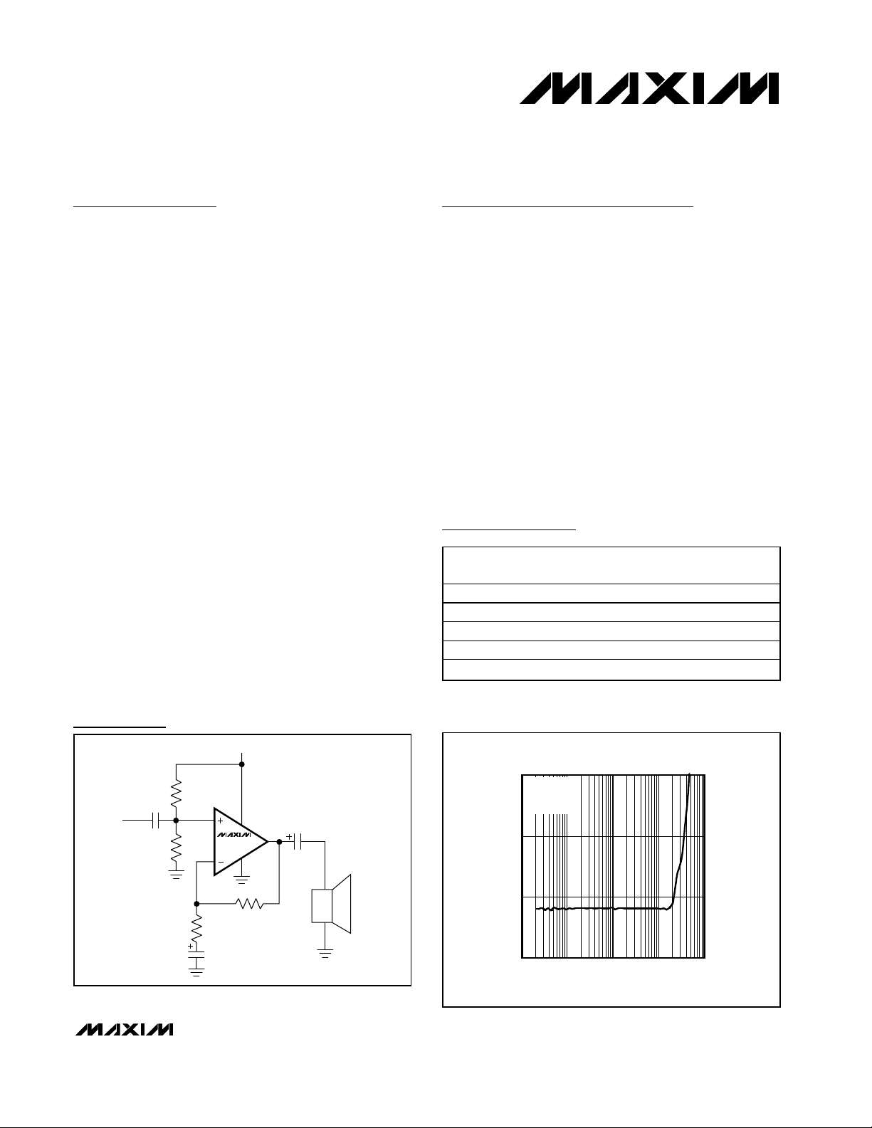
Typical Operating Circuit
PART TEMP RANGE
MAX4335EXT-T -40°C to +85°C 6 SC70-6 AAX
MAX4336EXT-T -40°C to +85°C 6 SC70-6 AAW
MAX4337EKA-T -40°C to +85°C 8 SOT23-8 AAIK
MAX4337EUA -40°C to +85°C 8 µMAX —
MAX4338EUB -40°C to +85°C 10 µMAX —
PINPACKAGE
MARK
TOP
R3
V
C1
IN
R4
V
CC
0.005
C2
MAX4335
MAX4336
R2
R1
C3
32Ω
0.004
THD + NOISE (%)
0.003
0.002
TOTAL HARMONIC DISTORTION
PLUS NOISE vs. FREQUENCY
RL = 10kΩ,
= 5V
V
CC
= 2V
V
OUT
P-P
10 100 10k1k 100k
FREQUENCY (Hz)
Page 2
MAX4335–MAX4338
SC70/SOT23-8, 50mA I
OUT
, Rail-to-Rail I/O
Op Amps with Shutdown/Mute
2 _______________________________________________________________________________________
ABSOLUTE MAXIMUM RATINGS
Stresses beyond those listed under “Absolute Maximum Ratings” may cause permanent damage to the device. These are stress ratings only, and functional
operation of the device at these or any other conditions beyond those indicated in the operational sections of the specifications is not implied. Exposure to
absolute maximum rating conditions for extended periods may affect device reliability.
Supply Voltage (VCCto GND) ..................................-0.3V to +6V
All Other Pins to GND ....................(GND - 0.3V) to (V
CC
+ 0.3V)
Output Short-Circuit Duration to V
CC
or GND............Continuous
Continuous Power Dissipation (T
A
= +70°C)
6-Pin SC70 (derate 3.1mW/°C above +70°C)...............245mW
8-Pin SOT23 (derate 9.1mW/°C above +70°C).............727mW
8-Pin µMAX (derate 4.5mW/°C above +70°C) ..............362mW
10-Pin µMAX (derate 5.6mW/°C above +70°C) .............444mW
Operating Temperature Range ...........................-40°C to +85°C
Junction Temperature......................................................+150°C
Storage Temperature Range .............................-65°C to +150°C
Lead Temperature (soldering, 10s) .................................+300°C
DC ELECTRICAL CHARACTERISTICS
(VCC= 2.7V, GND = 0, VCM= 0, V
OUT
= VCC/2, RL= ∞ to VCC/2, V
SHDN
= V
CC,
TA= +25°C, unless otherwise noted.)
Operating Supply Voltage Range V
Quiescent Supply Current (Per
Amplifier)
Input Offset Voltage V
Input Bias Current I
Input Offset Current I
Differential Input Resistance R
Input Common-Mode Voltage
Range
Common-Mode Rejection Ratio CMRR VCM = GND to V
Power-Supply Rejection Ratio PSRR VCC = 2.7V to 5.5V 70 90 dB
Output Resistance R
Large-Signal Voltage Gain A
Output Voltage Swing V
PARAMETER SYMBOL CONDITIONS MIN TYP MAX UNITS
CC
I
CC
OS
B
OS
IN(Diff)
V
CM
OUT
VOL
OUT
Inferred from PSRR Test 2.7 5.5 V
V
CC
V
CC
V
CM
VCM = GND to V
VCM = GND to V
|V
IN-
|
VIN-
Inferred from CMRR Test GND V
AVCL = 1V/V 0.05 Ω
VCC = 5V: RL = 10kΩ
V
OUT
VCC = 5V: RL = 100Ω
V
OUT
VCC = 2.7V: RL = 32Ω
V
OUT
VCC = 2.7V;
R
= 10kΩ
L
VCC = 2.7V;
R
= 32Ω
L
VCC = 5V;
R
= 10kΩ
L
VCC = 5V;
R
= 100Ω
L
= 5.5V 1.3 1.8
= 2.7 1.2
= GND to V
- V
| < 1.2V 500
IN+
- V
| > 1.2V 8.4
IN+
= 0.4V to 4.6V
= 0.5V to 4.5V
= 0.5V to 2.2V
CC
CC
CC
CC
±0.6 ±3 mV
±100 ±400 nA
60 80 dB
70 84
62 72
VCC - V
V
OL
VCC - V
V
OL
VCC - V
V
OL
VCC - V
V
OL
OH
OH
OH
OH
100
100
220 400
280 400
100
100
190 350
240 350
±7 ±30 nA
CC
95
mA
kΩ
V
dB
mV
Page 3
MAX4335–MAX4338
SC70/SOT23-8, 50mA I
OUT
, Rail-to-Rail I/O
Op Amps with Shutdown/Mute
_______________________________________________________________________________________ 3
DC ELECTRICAL CHARACTERISTICS (continued)
(VCC= 2.7V, GND = 0, VCM= 0, V
OUT
= VCC/2, RL= ∞ to VCC/2, V
SHDN
= V
CC,
TA= +25°C, unless otherwise noted.)
DC ELECTRICAL CHARACTERISTICS
(VCC= 2.7V, GND = 0, VCM= 0, V
OUT
= VCC/2, RL= ∞ to VCC/2, V
SHDN
= V
CC,
TA= -40°C to +85°C, unless otherwise noted.)
(Note 1)
(
)
)
Output Drive I
Short-Circuit Current I
SHDN Logic Levels
SHDN Leakage Current I
Output Leakage Current in
Shutdown
Shutdown Supply Current
(Per Amplifier)
PARAMETER SYMBOL CONDITIONS MIN TYP MAX UNITS
VCC = 2.7V;
I
SOURCE
I
OUT
SC
V
V
IL
I
SHDN
OUT
I
CC(SHDN
IH
IL
SINK
VCC = 5V;
I
SOURCE
I
SINK
Normal mode 0.7 x V
Shutdown mode 0.3 x V
VCC = 5V, GND < V
VCC = 5V, V
V
CC
SHDN = GND; VCC = 5V <0.04 0.5 µA
,
= 50mA
,
= 50mA
SHDN
VCC - V
V
VCC - V
V
SHDN
= 0, V
270 500
360 500
270 500
360 500
110 mA
0.01 0.5 µA
OL
OL
OUT
< V
OH
OH
CC
CC
= 0,
CC
0.5 µA
Operating Supply Voltage Range V
Quiescent Supply Current (Per
Amplifier)
Input Offset Voltage V
Input Bias Current I
Input Offset Current I
Input Common-Mode Voltage
Range
Common-Mode Rejection Ratio CMRR VCM = GND to V
Power-Supply Rejection Ratio PSRR VCC = 2.7V to 5.5V 64 dB
Large-Signal Voltage Gain A
PARAMETER SYMBOL CONDITIONS MIN TYP MAX UNITS
Inferred from PSRR test 2.7 5.5 V
CC
I
V
CC
OS
VOL
VCC = 5.5V 2.25 mA
V
OS
B
CM
= GND to V
CM
VCM = GND to V
VCM = GND to V
Inferred from CMRR test GND V
VCC = 5V: R
= 0.6V to 4.4V
V
OUT
VCC = 2.7V: RL = 32Ω,
V
= 0.6V to 2.1V
OUT
= 100Ω,
L
CC
CC
CC
CC
±6 mV
±600 nA
±60 nA
CC
50 dB
66
56
mV
V
V
dB
Page 4
MAX4335–MAX4338
SC70/SOT23-8, 50mA I
OUT
, Rail-to-Rail I/O
Op Amps with Shutdown/Mute
4 _______________________________________________________________________________________
DC ELECTRICAL CHARACTERISTICS (continued)
(VCC= 2.7V, GND = 0, VCM= 0, V
OUT
= VCC/2, RL = ∞ to VCC/2, V
SHDN
= V
CC,
TA= -40°C to +85°C, unless otherwise noted.)
(Note 1)
AC ELECTRICAL CHARACTERISTICS
(VCC= 2.7V, GND = 0, VCM= VCC/2, V
OUT
= VCC/2, V
SHDN
= V
CC,
A
VCL
= 1V/V, CL= 15pF, RL = ∞ to VCC/2,TA= +25°C, unless
otherwise noted.)
)
)
Output Voltage Swing V
Output Drive I
SHDN Logic Level
SHDN Leakage Current I
Output Leakage Current in
Shutdown
Shutdown Supply Current
(Per Amplifier)
PARAMETER SYMBOL CONDITIONS MIN TYP MAX UNITS
VCC = 2.7V;
= 32Ω
R
OUT
OUT
V
IH
V
IL
IL
I
OUT(SHDN
I
CC(SHDN
L
VCC = 5V;
= 100Ω
R
L
VCC = 2.7V;
I
I
VCC = 5V;
I
I
Normal mode 0.7 x V
Shutdown mode 0.3 x V
VCC = 5V, GND < V
V
V
V
,
SOURCE
= 50mA
SINK
,
SOURCE
= 50mA
SINK
= 5V, V
CC
CC
= 0; VCC = 5V 1 µA
SHDN
SHDN
SHDN
= 0, V
VCC - V
OH
V
OL
VCC - V
OH
V
OL
VCC - V
OH
V
OL
V
- V
CC
OH
V
OL
CC
< V
CC
= 0;
OUT
500
500
400
400
650
650
650
650
1µA
1µA
CC
mV
mV
V
Gain-Bandwidth Product GBWP 5 MHz
Full-Power Bandwidth FBWP V
Slew Rate SR 1.8 V/µs
Phase Margin PM 70 degrees
Gain Margin GM 18 dB
Total Harmonic Distortion THD
PARAMETER SYMBOL CONDITIONS MIN TYP MAX UNITS
= 2V
OUT
VCC = 5V, RL = 100Ω,
V
OUT
VCC = 5V, RL = 10kΩ, V
f = 10kHz
V
CC
= 32Ω,
R
L
V
OUT
= 2V
= 2.7V;
= 2V
P-P
P-P
P-P
, VCC = 5V 280 kHz
f = 1kHz 0.005
f = 10kHz 0.02
= 2V
OUT
f = 1kHz 0.01
f = 10kHz 0.03
P-P
,
0.003
%
Page 5
MAX4335–MAX4338
SC70/SOT23-8, 50mA I
OUT
, Rail-to-Rail I/O
Op Amps with Shutdown/Mute
_______________________________________________________________________________________ 5
AC ELECTRICAL CHARACTERISTICS (continued)
(VCC= +2.7V, GND = 0, VCM= VCC/2, V
OUT
= VCC/2, V
S HDN
= V
CC,
A
VCL
= 1V/V, CL= 15pF, RL = ∞ to VCC/2, TA= +25°C, unless
otherwise noted.)
Note 1: All devices are 100% production tested at T
A
= +25°C. All limits over temperature are guaranteed by design.
__________________________________________Typical Operating Characteristics
(VCC= 2.7V, GND = 0, VCM= 0, V
OUT
= VCC/2, RL = ∞ to VCC/2, V
S HDN
= V
CC,
TA= +25°C, unless otherwise noted.)
1.4
1.3
1.2
1.1
1.0
-40 10-15 35 60 85
MAX4335-8 toc01
TEMPERATURE (°C)
SUPPLY CURRENT (mA)
VCC = 5.5V
VCC = 2.7V
SUPPLY CURRENT PER AMPLIFIER
vs. TEMPERATURE
1.5
1.6
1.7
1.8
1.9
2.0
2.1
2.2
2.3
-40 -15 10 35 60 85
MAX4335-8 toc02
TEMPERATURE (°C)
MINIMUM OPERATING VOLTAGE (V)
MINIMUM OPERATING VOLTAGE
vs. TEMPERATURE
0
300
200
100
400
500
600
700
800
900
1000
MAX4335-8 toc03
TEMPERATURE (°C)
SUPPLY CURRENT (pA)
SHUTDOWN SUPPLY CURRENT
vs. TEMPERATURE
-40 -15 10 35 60 85
VCC = 5.5V
VCC = 2.7V
PARAMETER SYMBOL CONDITIONS MIN TYP MAX UNITS
Settling Time to 0.01% t
Crosstalk CT V
Input Capacitance C
Input Voltage-Noise Density e
Input Current-Noise Density I
Capacitive-Load Stability No sustained oscillation 200 pF
Shutdown Time t
Enable Time from Shutdown t
Power-Up Time t
S
IN
n
n
SHDN
ENABLE
ON
2V step 2 µs
OUT
= 2V
; f = 1kHz 100 dB
P-P
5pF
f = 10kHz 26
f = 1kHz
f = 10kHz 0.6
f = 1kHz
1µs
1µs
5µs
nV/√Hz
pA/√Hz
Page 6
MAX4335–MAX4338
SC70/SOT23-8, 50mA I
OUT
, Rail-to-Rail I/O
Op Amps with Shutdown/Mute
6 _______________________________________________________________________________________
MAX4335
8 toc04
)
Typical Operating Characteristics (continued)
(VCC= 2.7V, GND = 0, VCM= 0, V
OUT
= VCC/2, RL = ∞ to VCC/2, V
S HDN
= V
CC,
TA= +25°C, unless otherwise noted.)
INPUT OFFSET VOLTAGE
vs. TEMPERATURE
1.0
0.8
0.6
0.4
0.2
0
-0.2
-0.4
INPUT OFFSET VOLTAGE (mV)
-0.6
-0.8
-1.0
SC70
-40 -15 10 35 60 85
µMAX
TEMPERATURE (°C)
100
-
-50
-100
INPUT BIAS CURRENT (nA)
-150
-200
COMMON-MODE REJECTION RATIO
vs. TEMPERATURE
85
84
83
CMRR (dB)
82
81
80
-40 -15 10 35 60 85
TEMPERATURE (°C)
480
440
MAX4335-8 toc07
400
360
320
280
240
200
OUTPUT LOW VOLTAGE (mV)
160
120
INPUT BIAS CURRENT
vs. COMMON-MODE VOLTAGE
VCC = 2.7V VCC = 5.5V
50
0
0231 456
COMMON-MODE VOLTAGE (V)
OUTPUT LOW VOLTAGE
vs. TEMPERATURE
VCC = 5.5V
= 100Ω
R
L
VCC = 5.5V
= 100Ω
R
L
80
-40 -15 10 35 60 85
TEMPERATURE (°C)
VCC = 2.7V
= 100Ω
R
L
VCC = 2.7V
= 100Ω
R
L
200
150
MAX4335 toc05
100
50
0
-50
-100
INPUT BIAS CURRENT (nA)
-150
-200
-250
-40 -15 10 35 60 85
350
300
MAX4335-8 toc08
250
200
150
100
OUTPUT HIGH VOLTAGE (mV)
50
0
-40 -15 10 35 60 85
INPUT BIAS CURRENT
vs. TEMPERATURE
VCM = V
VCC = 5.5V
VCM = V
CC
VCC = 2.7V
TEMPERATURE (°C)
OUTPUT HIGH VOLTAGE
vs. TEMPERATURE
VCC = 5.5V
= 100Ω
R
L
VCC = 5.5V
= 100Ω
R
L
TEMPERATURE (°C)
VCM = 0
= 2.7V
V
CC
CC
VCM = 0
V
CC
VCC = 2.7V
= 100Ω
R
L
VCC = 2.7V
R
L
MAX4335-8 toc06
= 5.5V
MAX4335-8 toc09
= 100Ω
OUTPUT CURRENT vs. OUTPUT VOLTAGE
(SINKING)
250
200
150
100
OUTPUT CURRENT (mA)
50
0
0 1.6
VCC = 2.7V
0.80.4 1.2
OUTPUT VOLTAGE (V)
VCC = 5.5V
250
MAX4335 toc10
200
150
100
OUTPUT CURRENT (mA)
50
0
OUTPUT CURRENT vs. OUTPUT VOLTAGE
(SOURCING)
VCC = 5.5V
VCC = 2.7V
0 1.6
0.4 0.60.2 0.8 1.0 1.2 1.4
OUTPUT VOLTAGE (V
MAX4335 toc11
LARGE-SIGNAL GAIN vs. OUTPUT VOLTAGE
(SINKING, V
RL REFERENCED TO V
115
105
95
85
75
LARGE-SIGNAL GAIN (dB)
65
55
0 0.20.1 0.3 0.4 0.5
OUTPUT VOLTAGE (V)
CC
= 5.5V)
CC
RL = 100kΩ
RL = 1kΩ
RL = 100Ω
MAX4335 toc12
Page 7

MAX4335-8 toc19
FREQUENCY (Hz)
PSRR (dB)
100 1k 10k 100k 1M 10M
-110
-90
-70
-30
-50
-10
10
-100
-80
-60
-20
-40
0
POWER-SUPPLY REJECTION RATIO
vs. FREQUENCY
100
0.01
1k 10k 1M 10M
OUTPUT IMPEDANCE
vs. FREQUENCY
0.1
1
10
MAX4335-8 toc20
FREQUENCY (Hz)
OUTPUT IMPEDANCE (Ω)
100k
AV = 1
0.040
0.035
0.030
0.025
0.020
0.015
0.010
0.005
0
10 1k 10k100 100k
TOTAL HARMONIC DISTORTION AND
NOISE vs. FREQUENCY
MAX4335/8 toc21
FREQUENCY (Hz)
THD + NOISE (%)
VCC = 5V
V
OUT
= 2V
P-P
500kHz LOWPASS FILTER
R
L
= 10kΩ to VCC/2
MAX4335–MAX4338
SC70/SOT23-8, 50mA I
OUT
, Rail-to-Rail I/O
Op Amps with Shutdown/Mute
_______________________________________________________________________________________ 7
(Hz)
QUENCY (Hz)
Typical Operating Characteristics (continued)
(VCC= 2.7V, GND = 0, VCM= 0, V
OUT
= VCC/2, RL = ∞ to VCC/2, V
S HDN
= V
CC,
TA= +25°C, unless otherwise noted.)
LARGE-SIGNAL GAIN vs. OUTPUT VOLTAGE
120
(SOURCING, V
RL REFERENCED TO VCC/2
110
100
90
80
70
LARGE-SIGNAL GAIN (dB)
60
50
RL = 1kΩ
RL = 100Ω
0.1 0.2 0.3 0.4 0.5
OUTPUT VOLTAGE (V)
CC
RL = 100kΩ
= 5.5V)
LARGE-SIGNAL GAIN vs. TEMPERATURE
110
100
VCC = 2.7V
= 100kΩ
R
90
80
70
LARGE-SIGNAL GAIN (dB)
60
50
-40 10-15 35 60 85
L
VCC = 2.7V
= 32Ω
R
L
°
VCC = 5V
R
LARGE-SIGNAL GAIN vs. OUTPUT VOLTAGE
115
MAX4335 toc13
105
95
85
75
65
LARGE-SIGNAL GAIN (dB)
55
45
35
0.1 0.2 0.3 0.4 0.5
70
60
MAX4335 toc16
50
40
30
= 100Ω
L
20
GAIN (dB)
10
0
-10
-20
-30
100 1k 10k 100k 1M 10M
(SINKING, V
RL REFERENCED TO V
RL = 100kΩ
CC
RL = 100Ω
OUTPUT VOLTAGE (V)
GAIN AND PHASE vs. FREQUENCY
A
VCL
FREQUENCY
= 2.7V)
CC
RL = 1kΩ
= 1000V/V
MAX4335-8 toc17
LARGE-SIGNAL GAIN vs. OUTPUT VOLTAGE
(SOURCING, V
110
MAX4335 toc14
100
RL = 1kΩ
90
80
70
60
LARGE-SIGNAL GAIN (dB)
50
40
0.05 0.25 0.350.15 0.45 0.55 0.65 0.75
RL = 100kΩ
R
REFERENCED TO VCC/2
L
OUTPUT VOLTAGE (V)
GAIN AND PHASE vs. FREQUENCY
= 200pF)
(C
216
180
144
108
72
36
0
-36
-72
-108
-144
70
60
50
40
30
20
GAIN (dB)
10
PHASE (DEGREES)
0
-10
-20
-30
100 1k 10k 100k 1M 10M
L
A
FRE
= 1000V/V
VCL
= 2.7V)
CC
RL = 100Ω
RL = 32Ω
MAX4335-8 toc18
MAX4335 toc15
216
180
144
108
72
36
0
PHASE (DEGREES)
-36
-72
-108
-144
Page 8

MAX4335–MAX4338
SC70/SOT23-8, 50mA I
OUT
, Rail-to-Rail I/O
Op Amps with Shutdown/Mute
8 _______________________________________________________________________________________
____________________________Typical Operating Characteristics (continued)
(VCC= 2.7V, GND = 0, VCM= 0, V
OUT
= VCC/2, RL = ∞ to VCC/2, V
S HDN
= V
CC,
TA= +25°C, unless otherwise noted.)
TOTAL HARMONIC DISTORTION PLUS NOISE
vs. PEAK-TO-PEAK OUTPUT VOLTAGE
10
FREQUENCY = 10kHz
1
0.1
THD + NOISE (%)
0.01
RL = 100Ω
RL = 1kΩ
-60
MAX4335 toc22
-70
-80
R
= 100kΩ
L
-90
-100
CHANNEL-TO-CHANNEL ISOLATION
CHANNEL-TO-CHANNEL ISOLATION
vs. FREQUENCY
MAX4335/8 toc23
20mV/div
20mV/div
SMALL-SIGNAL TRANSIENT RESPONSE
(NONINVERTING)
IN
OUT
MAX4335 toc24
0.001
3.0 4.03.5 5.0 5.5
PEAK-TO-PEAK OUTPUT VOLTAGE (V)
4.5
-110
20mV/div
OUT
20mV/div
SMALL-SIGNAL TRANSIENT RESPONSE
IN
(INVERTING)
200ns/div
MAX4335 toc25
2V/div
OUT
2V/div
10 1k100 100k 10M
10k 1M
FREQUENCY (Hz)
LARGE-SIGNAL TRANSIENT RESPONSE
(NONINVERTING)
IN
2µs/div
200ns/div
LARGE-SIGNAL TRANSIENT RESPONSE
(INVERTING)
= 5V
V
CC
MAX4335 toc26
IN
2V/div
OUT
2V/div
2µs/div
VCC = 5V
MAX4335 toc27
Page 9

MAX4335–MAX4338
SC70/SOT23-8, 50mA I
OUT
, Rail-to-Rail I/O
Op Amps with Shutdown/Mute
_______________________________________________________________________________________ 9
Pin Description
Typical Application Circuit
L INPUT
V
REF
MUTE
R INPUT
PIN
MAX4337
MAX4335 MAX4336
SOT23 µMAX
1 1 3, 5 3, 5 3, 7 IN1+, IN2
2 2 4 4 4 GND Ground
3 3 2, 6 2, 6 2, 8 IN2-, IN2
4 4 1, 7 1, 7 1, 9 OUT1, OUT2 Output(s)
5 ——— — N.C. No Connection. Not internally connected.
— 5 —— 5, 6 SHDN1, SHDN2
6 6 8 8 10 V
MAX4338
MAX4338
NAME FUNCTION
+
Noninverting Input
Inverting Input
Drive SHDN low for shutdown. Drive SHDN
CC
high or connect to V
Positive Supply
for normal operation.
CC
Page 10

MAX4335–MAX4338
SC70/SOT23-8, 50mA I
OUT
, Rail-to-Rail I/O
Op Amps with Shutdown/Mute
10 ______________________________________________________________________________________
Applications Information
Package Power Dissipation
Warning: Due to the high-output-current drive, this op
amp can exceed the absolute maximum power-dissipation rating. As a general rule, as long as the peak cur-
rent is less than or equal to 50mA, the maximum package
power dissipation will not be exceeded for any of the
package types offered. There are some exceptions to this
rule, however. The absolute maximum power-dissipation
rating of each package should always be verified using
the following equations. The following equation gives an
approximation of the package power dissipation:
where: V
RMS
= the RMS voltage from VCCto V
OUT
when sourcing current
= the RMS voltage from V
OUT
to V
EE
when sinking current
I
RMS
= the RMS current flowing out of or into
the op amp and the load
θ = the phase difference between the
voltage and the current. For resistive
loads, COS θ = 1.
For example, the circuit in Figure 1 has a package
power dissipation of 220mW.
Therefore, P
IC(DISS)
= V
RMSIRMS
COS θ = 220mW
Adding a coupling capacitor improves the package
power dissipation because there is no DC current to
the load, as shown in Figure 2.
Therefore, P
IC(DISS)
= V
RMSIRMS
COS θ
= 45mW
The absolute maximum power-dissipation rating of the
package may be exceeded if the configuration in
Figure 1 is used with the MAX4335/MAX4336 amplifiers
at a high ambient temperature of 79°C (220.6mW/°C
plus a derating of 3.1mW/°C x 9°C = 247.9mW). Note
that the 247.9mW just exceeds the absolute maximum
power dissipation of 245mW for the 6-pin SC70 package.
Figure 1. A Circuit Example where the MAX4335/MAX4336 is
Dissipating High Power
Figure 2. A Circuit Example where Adding a Coupling
Capacitor Greatly Reduces the Power Dissipation of Its
Package
I +
P V I COS
IC DISS RMS RMS
()
≅θ
V
V V V
≅−
RMS CC DC
()
PEAK
−
2
V
=− −=
. . .
VV
55 275
1
2 043
2
I
≅=+
I
RMS
DC
PEAK
2
=
108
mA
RMS
.
VV
275
32
Ω
132
V
RMS
/
2
Ω
5.5V
R
C
V
= 2V
IN
P-P
MAX4335
R
MAX4336
32Ω
5.5V
R
C
IN
V
= 2V
IN
P-P
MAX4335
R
MAX4336
CC > 1
2π R
WHERE fL IS THE LOW-FREQUENCY CUTOFF
L fL
C
C
32Ω
V V V
≅−
RMS CC DC
()
V
PEAK
−
2
V
=− −=
. . .
VV
55 275
1
2 043
V
RMS
2
I
I +
≅=+
IA
RMS
DC
PEAK
0
2
=
22
mA
RMS
/
V
132
Ω
2
Page 11
MAX4335–MAX4338
SC70/SOT23-8, 50mA I
OUT
, Rail-to-Rail I/O
Op Amps with Shutdown/Mute
______________________________________________________________________________________ 11
Single-Supply Speaker Driver
The MAX4335/MAX4336 can be used as a single-supply speaker driver, as shown in the Typical Operating
Circuit. Capacitor C1 is used for blocking DC (a 0.1µF
ceramic capacitor can be used). When choosing resistors R3 and R4, take into consideration the input bias
current as well as how much supply current can be tolerated. Choose resistors R1 and R2 according to the
amount of gain and current desired. Capacitor C3
ensures unity gain for DC. A 10µF electrolytic capacitor
is suitable for most applications. The coupling capacitor C2 sets a low-frequency pole and is fairly large in
value. For a 32Ω load, a 100µF coupling capacitor
gives a low-frequency pole at 50Hz. The low-frequency
pole can be set according to the following equation:
ƒ = 1 / 2π (RLC2)
Rail-to-Rail Input Stage
Devices in the MAX4335–MAX4338 family of highoutput-current amplifiers have rail-to-rail input and output
stages designed for low-voltage, single-supply operation. The input stage consists of separate NPN and
PNP differential stages that combine to provide an
input common-mode range that extends 0.25V beyond
the supply rails. The PNP stage is active for input voltages close to the negative rail, and the NPN stage is
active for input voltages near the positive rail. The
switchover transition region, which occurs near VCC/2,
has been extended to minimize the slight degradation
in common-mode rejection ratio caused by mismatch of
the input pairs.
Since the input stage switches between the NPN and
PNP pairs, the input bias current changes polarity as the
input voltage passes through the transition region. Match
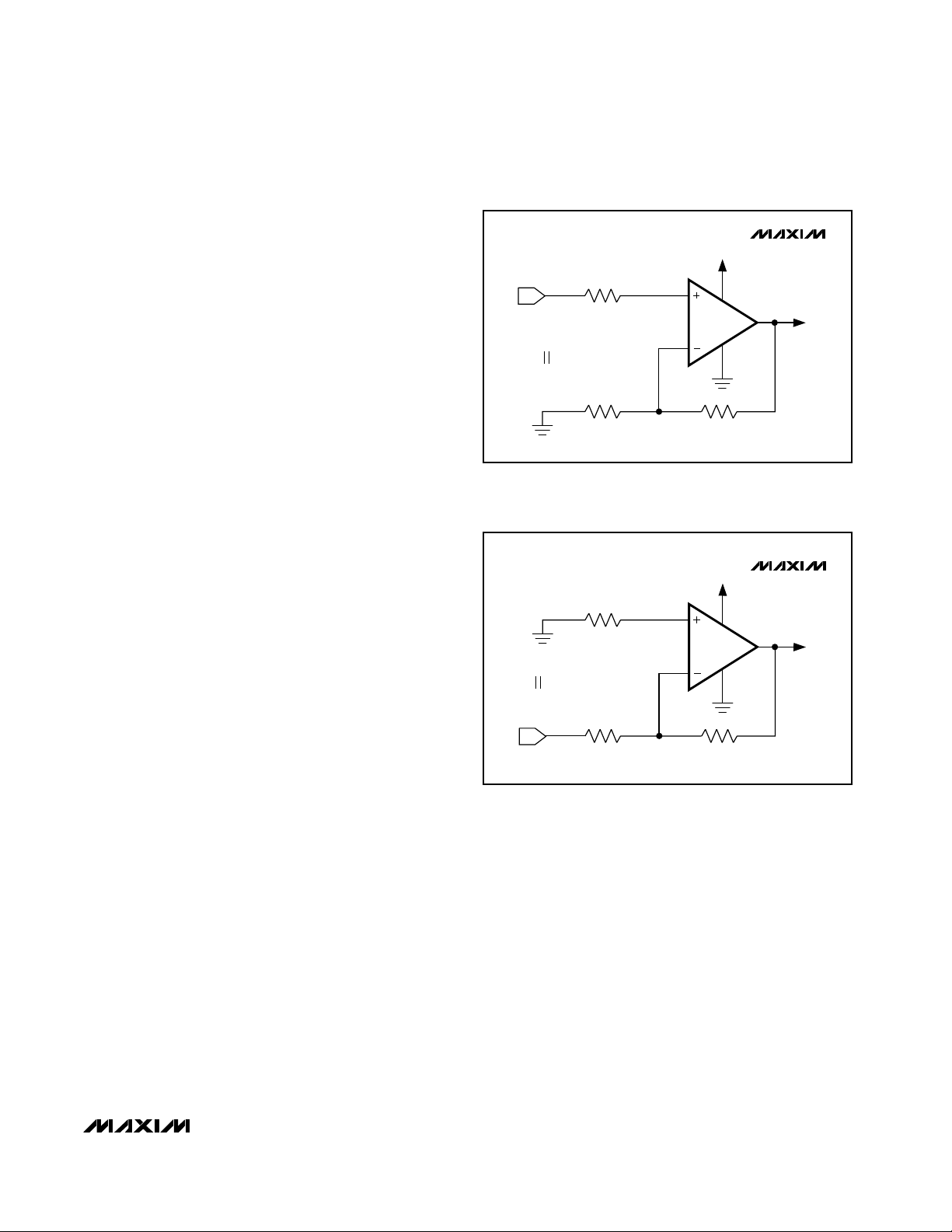
the effective impedance seen by each input to reduce the
offset error caused by input bias currents flowing through
external source impedances (Figures 3 and 5).
High source impedances, together with input capacitance, can create a parasitic pole that produces an
underdamped signal response. Reducing the input
impedance or placing a small (2pF to 10pF) capacitor
across the feedback resistor improves response.
The MAX4335–MAX4338’s inputs are protected from large
differential input voltages by 1kΩ series resistors and
back-to-back double diodes across the inputs (Figure 5).
For differential voltages less than 1.2V, input resistance is
typically 500kΩ. For differential input voltages greater
than 1.2V, input resistance is approximately 8.4kΩ. The
input bias current is given by the following equation:
I
BIAS
= (V
DIFF
- 1.2V) / 8.4kΩ
Rail-to-Rail Output Stage
The minimum output is within millivolts of ground for
single-supply operation, where the load is referenced
to ground (GND). Figure 6 shows the input voltage
range and the output voltage swing of a MAX4335 connected as a voltage follower. The maximum output voltage swing is load dependent; however, it is guaranteed
to be within 400mV of the positive rail (VCC= 2.7V)
even with maximum load (32Ω to VCC/2).
Driving Capacitive Loads
The MAX4335–MAX4338 have a high tolerance for
capacitive loads. They are stable with capacitive loads
up to 200pF. Figure 7 is a graph of the stable operating
region for various capacitive loads vs. resistive loads.
Figure 3. Reducing Offset Error Due to Bias Current
(Noninverting)
Figure 4. Reducing Offset Error Due to Bias Current (Inverting)
MAX4335–MAX4338
R3
R3 = R1 R2
R1 R2
MAX4335–MAX4338
R3
R3 = R1 R2
R1 R2
Page 12

MAX4335–MAX4338
SC70/SOT23-8, 50mA I
OUT
, Rail-to-Rail I/O
Op Amps with Shutdown/Mute
12 ______________________________________________________________________________________
Figures 8 and 9 show the transient response with
excessive capacitive loads (330pF), with and without
the addition of an isolation resistor in series with the
output. Figure 10 shows a typical noninverting capacitive-load-driving circuit in the unity-gain configuration.
The resistor improves the circuit’s phase margin by isolating the load capacitor from the op amp’s output.
Power-Up and Shutdown/Mute Modes
The MAX4336/MAX4338 have a shutdown option.
When the shutdown pin (SHDN) is pulled low, supply
current drops to 0.04µA per amplifier (VCC= 5V), the
amplifiers are disabled, and their outputs are placed in
a high-impedance state. Pulling SHDN high enables
the amplifier. In the dual MAX4338, the two amplifiers
shut down independently. Figure 11 shows the
MAX4336’s output voltage response to a shutdown
pulse. The MAX4335–MAX4338 typically settle within
5µs after power-up (Figure 12).
Power Supplies and Layout
The MAX4335–MAX4338 can operate from a single
2.7V to 5.5V supply. Bypass the power supply with a
0.1µF ceramic capacitor in parallel with at least 1µF.
Good layout improves performance by decreasing the
amount of stray capacitance at the op amps’ inputs
and outputs. Decrease stray capacitance by placing
external components close to the op amps’ input/output
pins, minimizing trace and lead lengths.
Thermal Overload Protection
The MAX4335–MAX4338 includes thermal overload
protection circuitry. When the junction temperature of
the device exceeds +140°C, the supply current drops
to 120µA per amplifier (VCC= 5V) and the outputs are
placed in a high-impedance state. The device returns
to normal operation when the junction temperature falls
to below +120°C.
Short-Circuit Current Protection
The MAX4335–MAX4338 incorporate a smart short-circuit protection feature. Figure 7 shows the output voltage region where the protection circuitry is active. A
fault condition occurs when I
OUT
> 110mA and V
OUT
>
1V (sinking current) or when I
OUT
> 110mA and (VCC-
V
OUT
) > 1V (sourcing current). When a fault is detected, the short-circuit protection circuitry is activated and
the output current is limited to 110mA, protecting the
device and the application circuitry. When the smart
short circuit is not active, the output current can safely
exceed 110mA (see the Output Current vs. Output
Voltage Graph in the Typical Operating Characteristics).
Figure 5. Input Protection Circuit
4.2kΩ
4.2kΩ
Page 13

MAX4335–MAX4338
SC70/SOT23-8, 50mA I
OUT
, Rail-to-Rail I/O
Op Amps with Shutdown/Mute
______________________________________________________________________________________ 13
(1V/div)
Figure 6. Rail-to-Rail Input/Output Range
Figure 7. Short-Circuit Protection
Figure 8. Capacitive-Load Stability
Figure 9. Small-Signal Transient Response with Excessive
Capacitive Load
OUT
(1V/div)
IN
V
OUT
V
CC
IN SOURCE MODE, SHORT-CIRCUIT PROTECTION CIRCUITRY IS NOT
ACTIVATED FOR (V
V
EXCEED 110mA.
- 1V
CC
1V
IN SINK MODE, SHORT-CIRCUIT PROTECTION CIRCUITRY IS NOT
ACTIVATED FOR V
EXCEED 110mA.
0
- V
) < 1V. OUTPUT CURRENT CAN SAFELY
CC
OUT
SHORT-CIRCUIT PROTECTION CIRCUITRY
LIMITS OUTPUT CURRENT TO 110mA
< 1V. OUTPUT CURRENT CAN SAFELY
OUT
1300
1200
1100
1000
900
800
700
600
500
400
CAPACITIVE LOAD (pF)
300
200
100
= 5.0V
V
CC
to VCC/2
R
L
UNSTABLE REGION
STABLE REGION
0
10 100k
100 1k 10k
RESISTIVE LOAD (Ω)
MAX4335-fig07
VCC = 3.0V, CL = 330pF
(20mV/div)
OUT
(20mV/div)
IN
= 100kΩ, R
R
L
= 0
ISO
1µs/div
MAX4335-fig08
Page 14

MAX4335–MAX4338
SC70/SOT23-8, 50mA I
OUT
, Rail-to-Rail I/O
Op Amps with Shutdown/Mute
14 ______________________________________________________________________________________
Figure 12. Shutdown Output Voltage Enable/Disable
Figure 13. Power-Up/Down Output Voltage
Figure 10. Small-Signal Transient Response with Excessive
Capacitive Load with Isolation Resistor
Figure 11. Capacitive-Load-Driving Circuit
VCC = 3.0V, CL = 330pF
= 100kΩ, R
R
L
ISO
= 39Ω
IN
(20mV/div)
OUT
(20mV/div)
1µs/div
MAX4335-fig11
SHDN
1V/div
R
MAX4336
V
CC
1V/div
ISO
C
L
MAX4335-fig12
OUT
1V/div
5µs/div
OUT
2V/div
5µs/div
Page 15

MAX4335–MAX4338
SC70/SOT23-8, 50mA I
OUT
, Rail-to-Rail I/O
Op Amps with Shutdown/Mute
______________________________________________________________________________________ 15
___________________Chip Information
MAX4335 TRANSISTOR COUNT: 1200
MAX4336 TRANSISTOR COUNT: 1200
MAX4337 TRANSISTOR COUNT: 2400
MAX4338 TRANSISTOR COUNT: 2400
PROCESS: BiCMOS
Pin Configurations
TOP VIEW
( ) MAX4335 ONLY
+
IN
16V
GND
MAX4335
2
MAX4336
-
34
SC70
CC
5 SHDN (N.C.)
OUTIN
OUT1
IN1-
IN1+
GND
1
2
3
4
MAX4337
SOT23/µMAX
87V
6
5
CC
OUT2
IN2-
IN2+
OUT1
IN1-
IN1+
GND
1
2
MAX4338
3
4
5
µMAX
10
V
CC
9
OUT2
IN2-
8
7
IN2+
6
SHDN2SHDN1
Page 16

MAX4335–MAX4338
SC70/SOT23-8, 50mA I
OUT
, Rail-to-Rail I/O
Op Amps with Shutdown/Mute
16 ______________________________________________________________________________________
Package Information
(The package drawing(s) in this data sheet may not reflect the most current specifications. For the latest package outline information,
go to www.maxim-ic.com/packages.)
0.6±0.1
0.6±0.1
8
1
TOP VIEW
ÿ 0.50±0.1
D
4X S
E H
BOTTOM VIEW
8
1
DIM
A
A1
A2
b
c
D
e
E
H
L
α
S
INCHES
MIN
-
0.002
0.030
0.010
0.005
0.116
0.0256 BSC
0.116
0.188
0.016
0∞
0.0207 BSC
MAX
0.043
0.006
0.037
0.014
0.007
0.120
0.120
0.198
0.026
6∞
MILLIMETERS
MAX
MIN
- 1.10
0.05 0.15
0.950.75
0.25 0.36
0.13 0.18
2.95 3.05
0.65 BSC
2.95 3.05
4.78
5.03
0.41
0.66
0.5250 BSC
8LUMAXD.EPS
6∞0∞
A2
e
FRONT VIEW
A1
A
b
c
L
SIDE VIEW
α
PROPRIETARY INFORMATION
TITLE:
PACKAGE OUTLINE, 8L uMAX/uSOP
21-0036
REV.DOCUMENT CONTROL NO.APPROVAL
1
J
1
SOT23, 8L.EPS
Page 17

MAX4335–MAX4338
SC70/SOT23-8, 50mA I
OUT
, Rail-to-Rail I/O
Op Amps with Shutdown/Mute
Maxim cannot assume responsibility for use of any circuitry other than circuitry entirely embodied in a Maxim product. No circuit patent licenses are
implied. Maxim reserves the right to change the circuitry and specifications without notice at any time.
Maxim Integrated Products, 120 San Gabriel Drive, Sunnyvale, CA 94086 408-737-7600 ____________________ 17
© 2001 Maxim Integrated Products Printed USA is a registered trademark of Maxim Integrated Products.
Package Information (continued)
(The package drawing(s) in this data sheet may not reflect the most current specifications. For the latest package outline information,
go to www.maxim-ic.com/packages.)
0.6±0.1
e
10
ÿ 0.50±0.1
1
0.6±0.1
TOP VIEW
D2
A2
D1
FRONT VIEW
4X S
H
BOTTOM VIEW
GAGE PLANE
A
b
α
A1
10
1
E2
E1
SIDE VIEW
INCHES
MAX
MIN
DIM
A1
A2 0.030 0.037 0.75 0.95
D1
D2
E1
E2
H
L
L1
b
e
c
S
α
c
L
L1
PROPRIETARY INFORMATION
TITLE:
PACKAGE OUTLINE, 10L uMAX/uSOP
0.043
-A
0.002
0.006
0.116
0.120
0.114
0.118
0.116
0.120
0.118
0.114
0.199
0.187
0.0275
0.0157
0.037 REF
0.007
0.0106
0.0197 BSC
0.0035
0.0078
0.0196 REF
6∞
0∞ 0∞ 6∞
21-0061
MILLIMETERS
MAX
MIN
-
1.10
0.05
0.15
2.95
3.05
3.00
2.89
3.05
2.95
2.89
3.00
4.75
5.05
0.40
0.70
0.940 REF
0.177
0.270
0.500 BSC
0.090
0.200
0.498 REF
REV.DOCUMENT CONTROL NO.APPROVAL
I
1
1
10LUMAX.EPS
Page 18

 Loading...