Maxim MAX4322EUA, MAX4322ESA, MAX4329ESD, MAX4327EUB, MAX4327ESD Datasheet
...
General Description
The MAX4322/MAX4323/MAX4326/MAX4327/MAX4329
family of operational amplifiers combines wide bandwidth
and excellent DC accuracy with Rail-to-Rail
®
operation at
the inputs and outputs. These devices require only 650µA
per amplifier and operate from either a single supply
(+2.4V to +6.5V) or dual supplies (±1.2V to ±3.25V). These
unity-gain-stable amplifiers are capable of driving 250Ω
loads and have a 5MHz gain-bandwidth product. The
MAX4323 and MAX4327 feature a low-power shutdown
mode that reduces supply current to 25µA and places the
outputs in a high-impedance state.
With their rail-to-rail input common-mode range and
output swing, these amplifiers are ideal for low-voltage,
single-supply operation. In addition, low offset voltage
and high speed make them the ideal signal-conditioning stages for precision, low-voltage data-acquisition
systems. The MAX4322/MAX4323 are available in
space-saving SOT23 packages.
________________________Applications
Battery-Powered Instruments
Portable Equipment
Data-Acquisition Systems
Signal Conditioning
Low-Power, Low-Voltage Applications
____________________________Features
♦ SOT23 Packages (MAX4322/MAX4323)
♦ +2.4V to +6.5V Single-Supply Operation
♦ Rail-to-Rail Input Common-Mode Voltage Range
♦ Rail-to-Rail Output Voltage Swing
♦ 5MHz Gain-Bandwidth Product
♦ 650µA Quiescent Current per Amplifier
♦ 700µV Offset Voltage
♦ No Phase Reversal for Overdriven Inputs
♦ Drive 250Ω Loads
♦ 25µA Shutdown Mode (MAX4323/MAX4327)
♦ Unity-Gain Stable for Capacitive Loads
up to 500pF
MAX4322/MAX4323/MAX4326/MAX4327/MAX4329
Single/Dual/Quad, Low-Cost, SOT23,
Low-Power, Rail-to-Rail I/O Op Amps
________________________________________________________________ Maxim Integrated Products 1
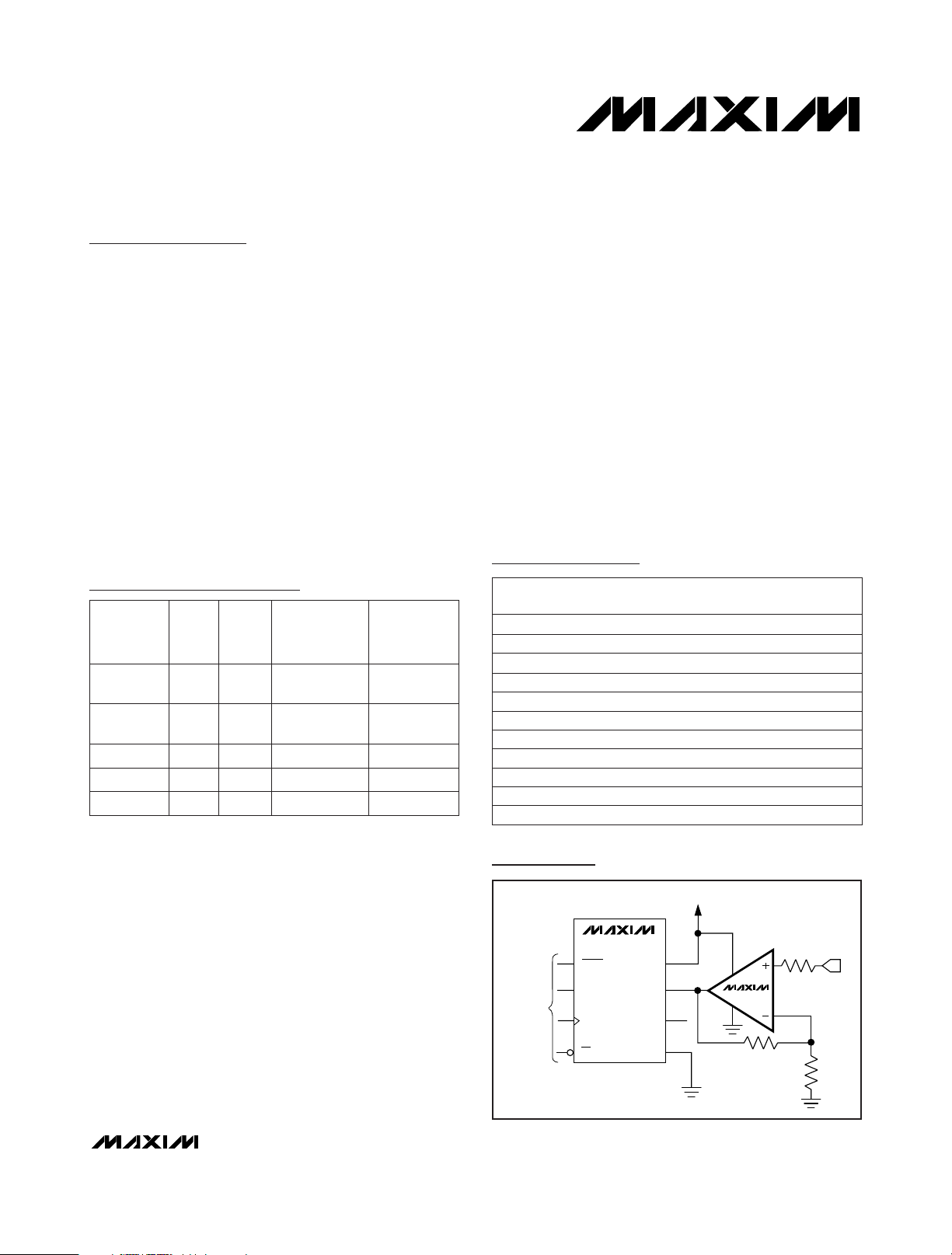
Typical Operating Circuit
19-1380; Rev 2a; 12/99
PART
MAX4322EUK-T
MAX4322ESA
-40°C to +85°C
-40°C to +85°C
TEMP. RANGE
PIN-
PACKAGE
5 SOT23-5
8 SO
Ordering Information
Pin Configurations appear at end of data sheet.
TOP
MARK
ACGE
—
BW
(MHz)
NO. OF
AMPS
MAX4322 5 1
PART
MAX4323 5 1
MAX4329 5 4
PIN-
PACKAGE
5 SOT23-5,
8 µMAX/SO
8 µMAX/SO/
6 SOT23-6
14 SO
Rail-to-Rail is a registered trademark of Nippon Motorola, Ltd.
SHUTDOWN
—
Yes
—
—MAX4326 5 2 8 µMAX/SO
YesMAX4327 5 2
10 µMAX, 14 SO
MAX4323ESA
-40°C to +85°C 8 SO —
MAX4323EUA -40°C to +85°C 8 µMAX —
MAX4322EUA -40°C to +85°C 8 µMAX —
MAX4326EUA
-40°C to +85°C 8 µMAX —
MAX4326ESA -40°C to +85°C 8 SO —
MAX4327ESD -40°C to +85°C 14 SO —
MAX4327EUB
-40°C to +85°C 10 µMAX —
MAX4329ESD
-40°C to +85°C 14 SO —
Selector Guide
MAX187
MAX4322
SHDN
3
1
2
4
5
6
8
7
V
DD
+5V
AIN
VREF
GND
DOUT
SERIAL
INTERFACE
SCLK
CS
MAX4323EUT -40°C to +85°C 6 SOT23-6 AAEC
For free samples and the latest literature, visit www.maxim-ic.com or phone 1-800-998-8800.
For small orders, phone 1-800-835-8769.

MAX4322/MAX4323/MAX4326/MAX4327/MAX4329
Single/Dual/Quad, Low-Cost, SOT23,
Low-Power, Rail-to-Rail I/O Op Amps
2 _______________________________________________________________________________________
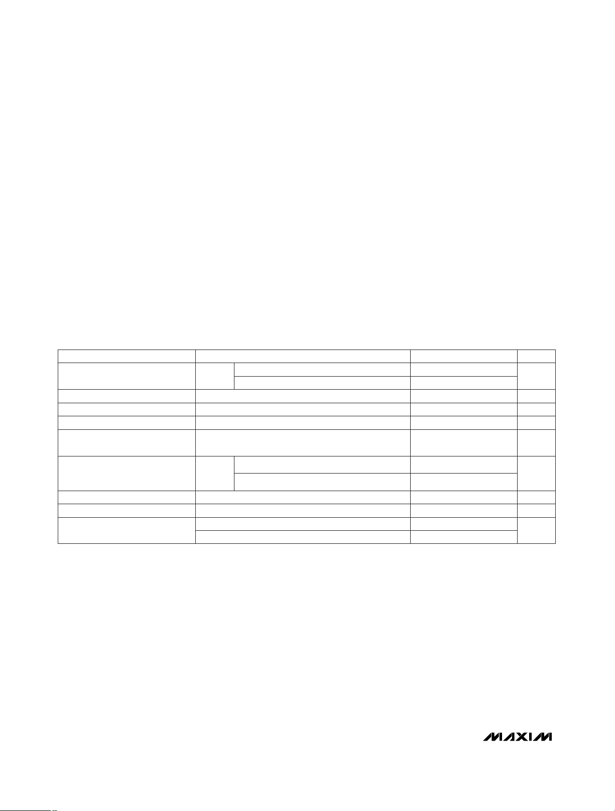
ABSOLUTE MAXIMUM RATINGS
DC ELECTRICAL CHARACTERISTICS—TA= +25°C
(VCC= +5.0V, VEE= 0, VCM= 0, V
OUT
= VCC/ 2, SHDN = V
CC,
RLtied to VCC/ 2, unless otherwise noted.)
Stresses beyond those listed under “Absolute Maximum Ratings” may cause permanent damage to the device. These are stress ratings only, and functional
operation of the device at these or any other conditions beyond those indicated in the operational sections of the specifications is not implied. Exposure to
absolute maximum rating conditions for extended periods may affect device reliability.
Supply Voltage (VCC-VEE) ..................................................+7.5V
All Other Pins ...................................(V
CC
+ 0.3V) to (VEE- 0.3V)
Output Short-Circuit Duration.....................................Continuous
(short to either supply)
Continuous Power Dissipation (T
A
= +70°C)
5-pin SOT23-5 (derate 7.1mW/°C above +70°C) .........571mW
6-pin SOT23 (derate 7.1mW/°C Above + 70°C) ...........571mW
8-pin SO (derate 5.88mW/°C above +70°C).................471mW
8-pin µMAX (derate 4.10mW/°C above +70°C) ............330mW
10-pin µMAX (derate 5.6mW/°C above +70°C) ............444mW
14-pin SO (derate 8.00mW/°C above +70°C)...............640mW
Operating Temperature Range
MAX432_E__ ....................................................-40°C to +85°C
Maximum Junction Temperature .....................................+150°C
Storage Temperature Range .............................-65°C to +160°C
Lead Temperature (soldering, 10sec) .............................+300°C
V
CM
= VEE, V
CC
CONDITIONS
nA±1 ±12Input Offset Current
nA±50 ±150Input Bias Current
Ω0.1Output Resistance
kΩ500Differential Input Resistance
dB66 100Power-Supply Rejection Ratio
UNITSMIN TYP MAXPARAMETER
V
OUT
= 0.4V to 4.6V, RL= 250Ω 70 86
VV
EE
V
CC
Common-Mode Input
Voltage Range
±1.2 ±2.50
±0.7 ±2.0
Input Offset Voltage mV
VCM= VEE, V
CC
-1.5V < V
DIFF
< 1.5V
Inferred from CMRR test
VCC= 2.4V to 6.5V
AV= +1V/V
V
EE
≤
V
CM
≤
V
CC
62 94
Common-Mode Rejection Ratio dB
V
OUT
= 0.25V to 4.75V, RL= 100kΩ 106
VCM=
VEE, V
CC
MAX432_ESA/MAX4327ESD
All other packages
MAX432_ESA/MAX4327ESD
dBLarge-Signal Voltage Gain
All other packages 60 91

MAX4322/MAX4323/MAX4326/MAX4327/MAX4329
Single/Dual/Quad, Low-Cost, SOT23,
Low-Power, Rail-to-Rail I/O Op Amps
_______________________________________________________________________________________ 3
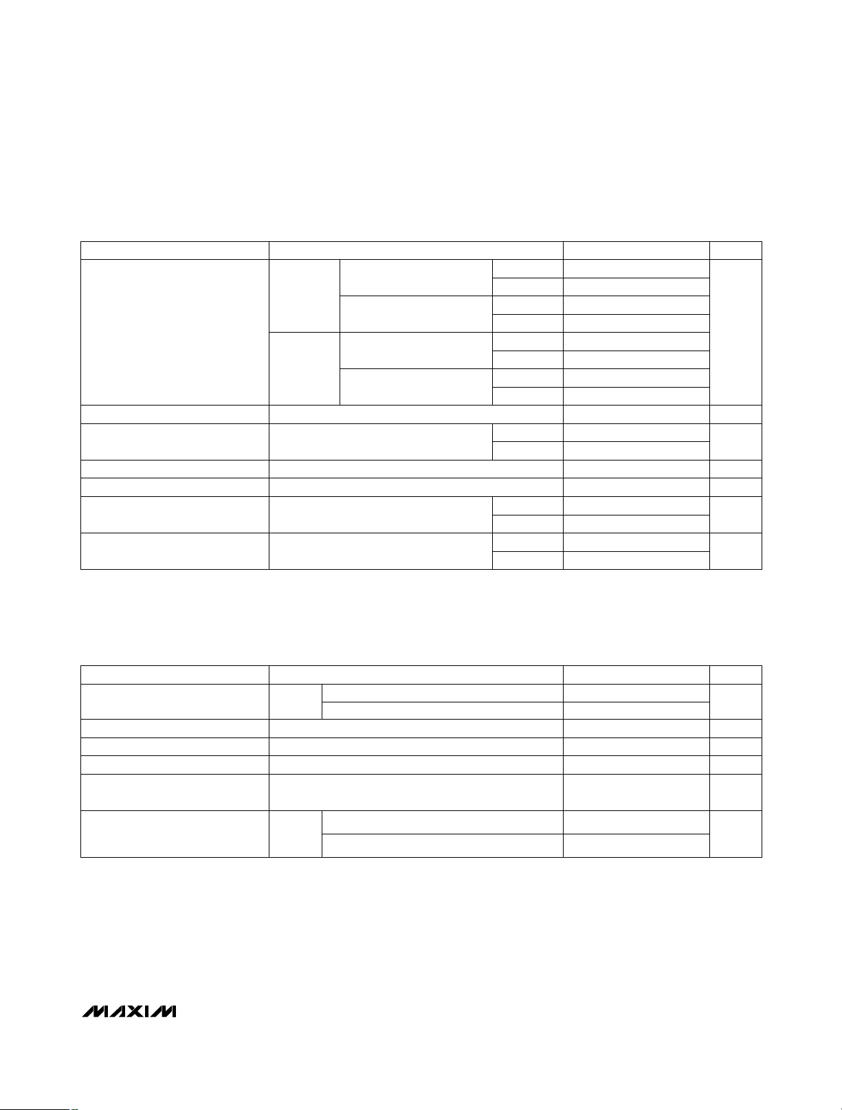
DC ELECTRICAL CHARACTERISTICS—TA= -40°C to +85°C
(VCC= +5V, VEE= 0, VCM= 0, V
OUT
= VCC/ 2, SHDN = V
CC,
RLtied to VCC/ 2, unless otherwise noted.) (Note 1)
DC ELECTRICAL CHARACTERISTICS—TA= +25°C (continued)
(VCC= +5V, VEE= 0, VCM= 0, V
OUT
= VCC/ 2, SHDN = V
CC,
RLtied to VCC/ 2, unless otherwise noted.)
RL= 100kΩ
CONDITIONS
20
V2.4 6.5Operating Supply-Voltage Range
200 300
12
VOL- V
EE
100 200
MAX4322/
MAX4323
mA50Output Short-Circuit Current
UNITSMIN TYP MAXPARAMETER
VCC- V
OH
VOL- V
EE
VCC- V
OH
RL= 250Ω
VCC- V
OH
VOL- V
EE
VCC- V
OH
RL= 250Ω
RL= 100kΩ
25
mV
220 350
15
VOL- V
EE
Output Voltage Swing
120 250
MAX4326/
MAX4327/
MAX4329
Inferred from PSRR test
VCC= 2.4V
VCM= V
OUT
= VCC/ 2 µA
650
VCC= 5V 725 1100
Supply Current per Amplifier
MAX432_ESA/MAX4327ESD
VEE≤
VCM≤
V
CC
CONDITIONS
59
VCM= VEE, V
CC
Inferred from CMRR test VV
EE
V
CC
Common-Mode Input
Voltage Range
Common-Mode Rejection Ratio
nA±20Input Offset Current
µV/°C±2
dB
All other packages
Input Offset Voltage Tempco
54
UNITSMIN TYP MAX
VCM= VEE, V
CC
nA±180Input Bias Current
mV
MAX4323/MAX4327 V
0.8
SHDN Logic Threshold
2.0
µA±1 ±4
SHDN Input Current
Low
High
MAX4323/MAX4327
VCC= 5V 40 60
Shutdown Supply Current
per Amplifier
VCC= 2.4V
SHDN > 0.8V, MAX4323/MAX4327
µA
25
PARAMETER
All other packages
VCM=
VEE, V
CC
Input Offset Voltage
±6.0
MAX432_ESA/MAX4327ESD ±3.0

MAX4322/MAX4323/MAX4326/MAX4327/MAX4329
Single/Dual/Quad, Low-Cost, SOT23,
Low-Power, Rail-to-Rail I/O Op Amps
4 _______________________________________________________________________________________
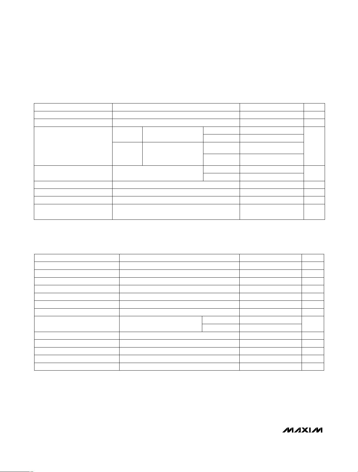
DC ELECTRICAL CHARACTERISTICS —TA= -40°C to +85°C (continued)
(VCC= +5V, VEE= 0, VCM= 0, V
OUT
= VCC/ 2, SHDN = V
CC,
RLtied to VCC/ 2, unless otherwise noted.) (Note 1)
f = 10kHz, V
OUT
= 2Vp-p, AV= +1V/V
VCC= 0 to 3V step
64 degrees
AV= +1V/V, V
OUT
= 2V step
CONDITIONS
µs
5
Phase Margin
MHzGain-Bandwidth Product
12
%0.003
dB
Total Harmonic Distortion
Gain Margin
Settling Time to 0.01% 2.0
µs1Turn-On Time
V/µsSlew Rate 2
UNITSMIN TYP MAXPARAMETER
AC ELECTRICAL CHARACTERISTICS
(VCC= +5V, VEE= 0, VCM= V
OUT
= V
CC
/ 2, SHDN = V
CC,
TA= +25°C unless otherwise noted.)
V
OUT
= 0.4V to 4.6V, RL= 250Ω
VCC= 2.4V to 6.5V
RL= 250Ω
CONDITIONS
dB66
dB62Power-Supply Rejection Ratio
Output Voltage Swing mV
350
MAX4322/
MAX4323
250
UNITSMIN TYP MAXPARAMETER
VCC- V
OH
VOL- V
EE
400
MAX4326/
MAX4327/
MAX4329
pF3Input Capacitance
f = 1kHz
nV/√Hz
22Input Noise Voltage Density
f = 1kHz pA0.4Input Noise Current Density
dB135Amp-Amp Isolation
AV= +1V/V pF250Capacitive Load Stability
Note 1: All devices are 100% tested at TA= +25°C. All temperature limits are guaranteed by design.
MAX4323/MAX4327 V
0.8
SHDN Logic Threshold
Large-Signal Voltage Gain
RL= 250Ω
VCC- V
OH
300VOL- V
EE
2.0
MAX4323/MAX4327 µA±5
SHDN Input Current
V2.4 6.5Operating Supply-Voltage Range
Low
High
VCM= VCC/ 2 mA1.2Supply Current per Amplifier
SHDN ≤ 0.8V, MAX4323/MAX4327
µA70
Shutdown Supply Current
per Amplifier
µs
1
SHDN Delay
MAX4323/MAX4327
0.2
Enable
Disable
 Loading...