Maxim MAX4305EUK-T, MAX4305ESA, MAX4304EUK-T, MAX4304ESA, MAX4105EUK-T Datasheet
...
For free samples & the latest literature: http://www.maxim-ic.com, or phone 1-800-998-8800.
For small orders, phone 1-800-835-8769.
General Description
The MAX4104/MAX4105/MAX4304/MAX4305 op amps
feature ultra-high speed, low noise, and low distortion in
a SOT23 package. The unity-gain-stable MAX4104
requires only 20mA of supply current while delivering
625MHz bandwidth and 400V/µs slew rate. The
MAX4304, compensated for gains of +2V/V or greater,
delivers a 730MHz bandwidth and a 1000V/µs slew
rate. The MAX4105 is compensated for a minimum gain
of +5V/V and delivers a 410MHz bandwidth and a
1400V/sec slew rate. The MAX4305 has +10V/V minimum gain compensation and delivers a 340MHz bandwidth and a 1400V/µs slew rate.
Low voltage noise density of 2.1nV/√Hz and -88dBc
spurious-free dynamic range make these devices ideal
for low-noise/low-distortion video and telecommunications applications. These op amps also feature a wide
output voltage swing of ±3.7V and ±70mA output currentdrive capability. For space-critical applications, they
are available in a miniature 5-pin SOT23 package.
________________________Applications
Video ADC Preamp
Pulse/RF Telecom Applications
Video Buffers and Cable Drivers
Ultrasound
Active Filters
ADC Input Buffers
Features
♦ Low 2.1nV/√Hz Voltage Noise Density
♦ Ultra-High 740MHz -3dB Bandwidth (MAX4304,
A
VCL
= 2V/V)
♦ 100MHz 0.1dB Gain Flatness (MAX4104/4105)
♦ 1400V/µs Slew Rate (MAX4105/4305)
♦ -88dBc SFDR (5MHz, R
L
= 100Ω) (MAX4104/4304)
♦ High Output Current Drive: ±70mA
♦ Low Differential Gain/Phase Error: 0.01%/0.01°
(MAX4104/4304)
♦ Low ±1mV Input Offset Voltage
♦ Available in Space-Saving 5-Pin SOT23 Package
MAX4104/MAX4105/MAX4304/MAX4305
740MHz, Low-Noise, Low-Distortion
Op Amps in SOT23-5
________________________________________________________________
Maxim Integrated Products
1
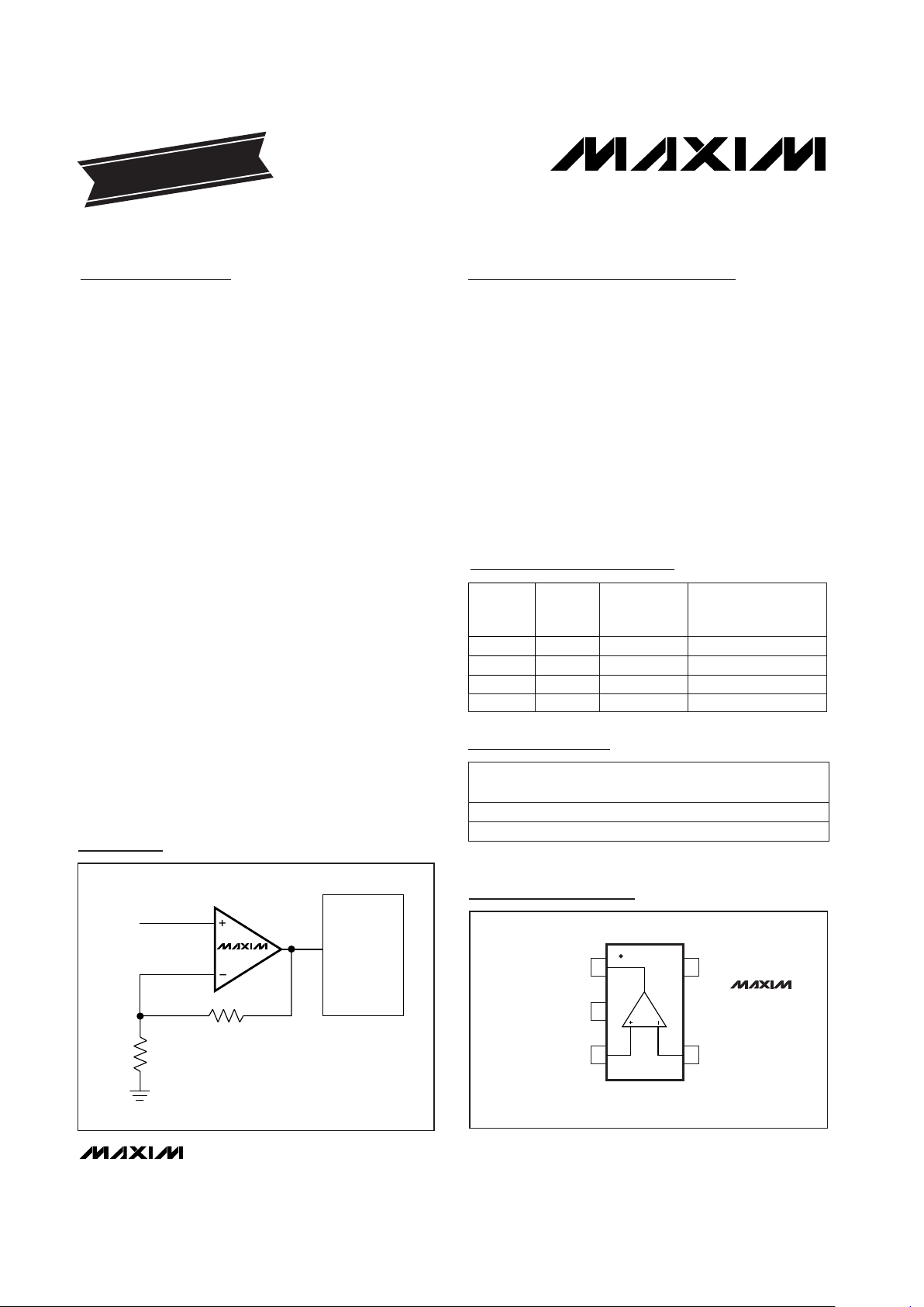
MAX4304
8 to 16-BIT
HIGH-SPEED
ADC
INPUT
330Ω
ADC BUFFER WITH GAIN (A
VCL
= 2V/V)
330Ω
Typical Application Circuit
19-4757; Rev 3; 10/98
PART
MAX4104ESA
MAX4104EUK-T -40°C to +85°C
-40°C to +85°C
TEMP. RANGE
PIN-
PACKAGE
8 SO
5 SOT23-5
EVALUATION KIT MANUAL
FOLLOWS DATA SHEET
Ordering Information
Selector Guide
SOT
TOP MARK
—
ACCO
PART
MAX4104
MAX4304
MAX4105 5
2
1
MINIMUM
STABLE
GAIN (V/V)
BANDWIDTH
(MHz)
625
740
410
MAX4305 10 340
PIN-PACKAGE
5-pin SOT23, 8-pin SO
5-pin SOT23, 8-pin SO
5-pin SOT23, 8-pin SO
5-pin SOT23, 8-pin SO
V
EE
IN-IN+
15V
CC
OUT
SOT23-5
2
34
MAX4104
MAX4105
MAX4304
MAX4305
TOP VIEW
Pin Configurations
Pin Configurations continued at end of data sheet.
Ordering Information continued at end of data sheet.

MAX4104/MAX4105/MAX4304/MAX4305
740MHz, Low-Noise, Low-Distortion
Op Amps in SOT23-5
2 _______________________________________________________________________________________
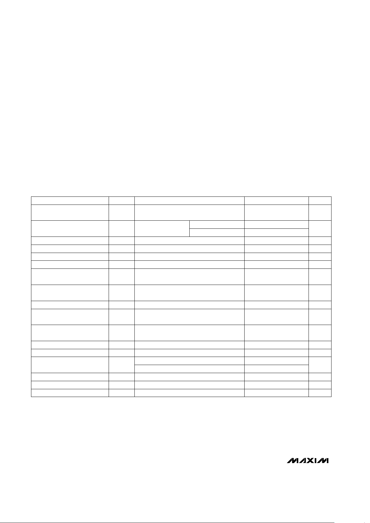
ABSOLUTE MAXIMUM RATINGS
DC ELECTRICAL CHARACTERISTICS
(VCC= +5V, VEE= -5V, VCM= 0, RL= 100kΩ, TA= T
MIN
to T
MAX
, unless otherwise noted. Typical values are at TA= +25°C.)
Stresses beyond those listed under “Absolute Maximum Ratings” may cause permanent damage to the device. These are stress ratings only, and functional
operation of the device at these or any other conditions beyond those indicated in the operational sections of the specifications is not implied. Exposure to
absolute maximum rating conditions for extended periods may affect device reliability.
Supply Voltage (VCCto VEE)................................................+12V
Voltage on Any Pin to Ground..........(V
EE
- 0.3V) to (VCC+ 0.3V)
Short-Circuit Duration (V
OUT
to GND)........................Continuous
Continuous Power Dissipation (T
A
= +70°C)
5-pin SOT23 (derate 7.1mW/°C above +70°C)...........571mW
8-pin SO (derate 5.9mW/°C above +70°C).................471mW
Operating Temperature Range ...........................-40°C to +85°C
Storage Temperature Range.............................-65°C to +150°C
Lead Temperature (soldering, 10sec).............................+300°C
V
OUT
= 0
RL= short to ground
Guaranteed by PSRR test
RL= 30Ω
RL= 100kΩ
VCC= 3.5V to 5.5V
-2.8V ≤ VCM≤ 4.1V
-2.8V ≤ V
OUT
≤ 2.8V, RL= 100Ω
V
OUT
= 0
Guaranteed by CMRR test
Either input
-0.8V ≤ VIN≤ 0.8V
VEE= -3.5V to -5.5V
CONDITIONS
Ω9Z
OUT
Open-Loop Output Impedance
mA80I
SC
Short-Circuit Output Current
mA±53 ±70I
OUT
Output Current Drive
±3.0 -3.5 to +3.4
V
±3.5 -3.7 to +3.8
V
OUT
Output Voltage Swing
dB55 65A
VOL
Open-Loop Gain
mA20 27I
S
Quiescent Supply Current
dB55 65PSRR-
Negative Power-Supply
Rejection Ratio
mV
1 6
V
OS
V±3.5 ±5 ±5.5VCC/V
EE
Operating Supply Voltage
Range
dB75 85PSSR+
Positive Power-Supply Rejection
Ratio
dB80 95CMRRCommon-Mode Rejection Ratio
V-2.8 +4.1V
CM
Input Common-Mode Voltage
Range
MΩ1.5R
IN
Common-Mode Input
Resistance
1 8
µV/°CTCV
OS
Input Offset-Voltage Drift
µA32 70I
B
kΩ6R
IN
Differential Input Resistance
UNITSMIN TYP MAXSYMBOLPARAMETER
Input Offset Voltage
Input Bias Current
MAX4_0_EUK
2.5
MAX4_0_ESA
Input Offset Current µA0.5 5.0I
OS
RL= 100Ω

MAX4104/MAX4105/MAX4304/MAX4305
740MHz, Low-Noise, Low-Distortion
Op Amps in SOT23-5
_______________________________________________________________________________________ 3
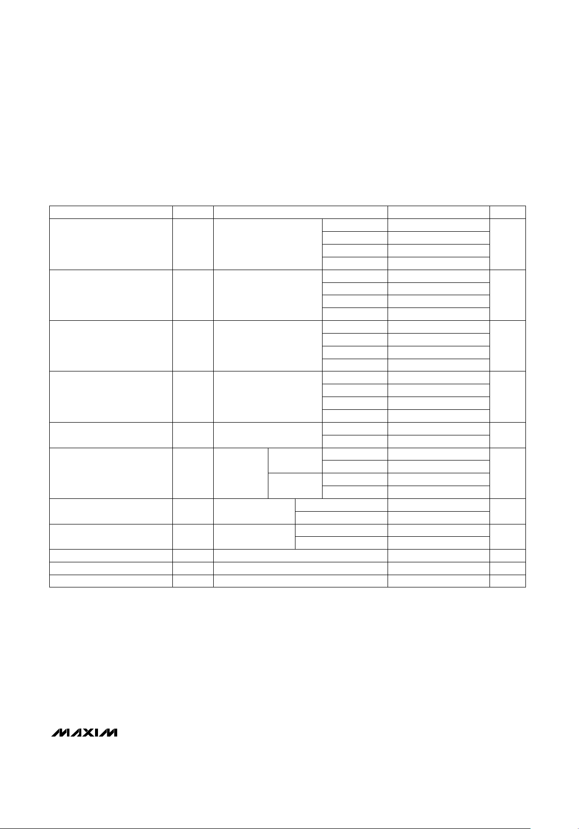
AC ELECTRICAL CHARACTERISTICS
(VCC= +5V, VEE= -5V, VCM= 0, RL= 100Ω; AV= +1V/V for MAX4104, +2V/V for MAX4304, +5V/V for MAX4105, +10V/V for MAX4305;
T
A
= +25°C; unless otherwise noted.)
CONDITIONS
MHz
625
BW
(-3dB)
-3dB Bandwidth
UNITSMIN TYP MAXSYMBOLPARAMETER
20
V
OUT
= 2Vp-p
f = 1MHz
f = 10MHz
f = 1MHz
Ω1Z
OUT
Output Impedance
pA/√Hz
3.1i
n
Input Current Noise Density
nV/√Hz
2.1e
n
Input Voltage Noise Density
nst
S
Settling Time to 0.1%
%
0.01
DGDifferential Gain Error
V
OUT
= 100mVp-p
MAX4104
MAX4304
MAX4105
MAX4305 340
410
740
MAX4305
MHz
100
BW
(0.1)
0.1dB Bandwidth
MAX4104
V
OUT
= 100mVp-p
MAX4304
MAX4105
70
80
60
MAX4305
MHz
115
FPBWFull-Power Bandwidth
MAX4104
V
OUT
= 2Vp-p
MAX4304
MAX4105
320
370
285
MAX4305
V/µs
400
SRSlew Rate
MAX4104
V
OUT
= 2Vp-p
MAX4304
MAX4105
1400
1400
1000
to 0.1%
25to 0.01%
-88
V
OUT
=2Vp-p
fC = 5MHz
-67fC = 20MHz
dBcSFDR
Spurious-Free
Dynamic Range
-74fC = 5MHz
-61fC = 20MHz
MAX4104/
MAX4304
MAX4105/
MAX4305
MAX4104/MAX4304
NTSC, RL= 150Ω
MAX4105/MAX4305 0.02
MAX4105/MAX4305
MAX4104/MAX4304
NTSC, RL= 150Ω degrees
0.02
0.01
DPDifferential Phase Error

MAX4104/MAX4105/MAX4304/MAX4305
740MHz, Low-Noise, Low-Distortion
Op Amps in SOT23-5
4 _______________________________________________________________________________________
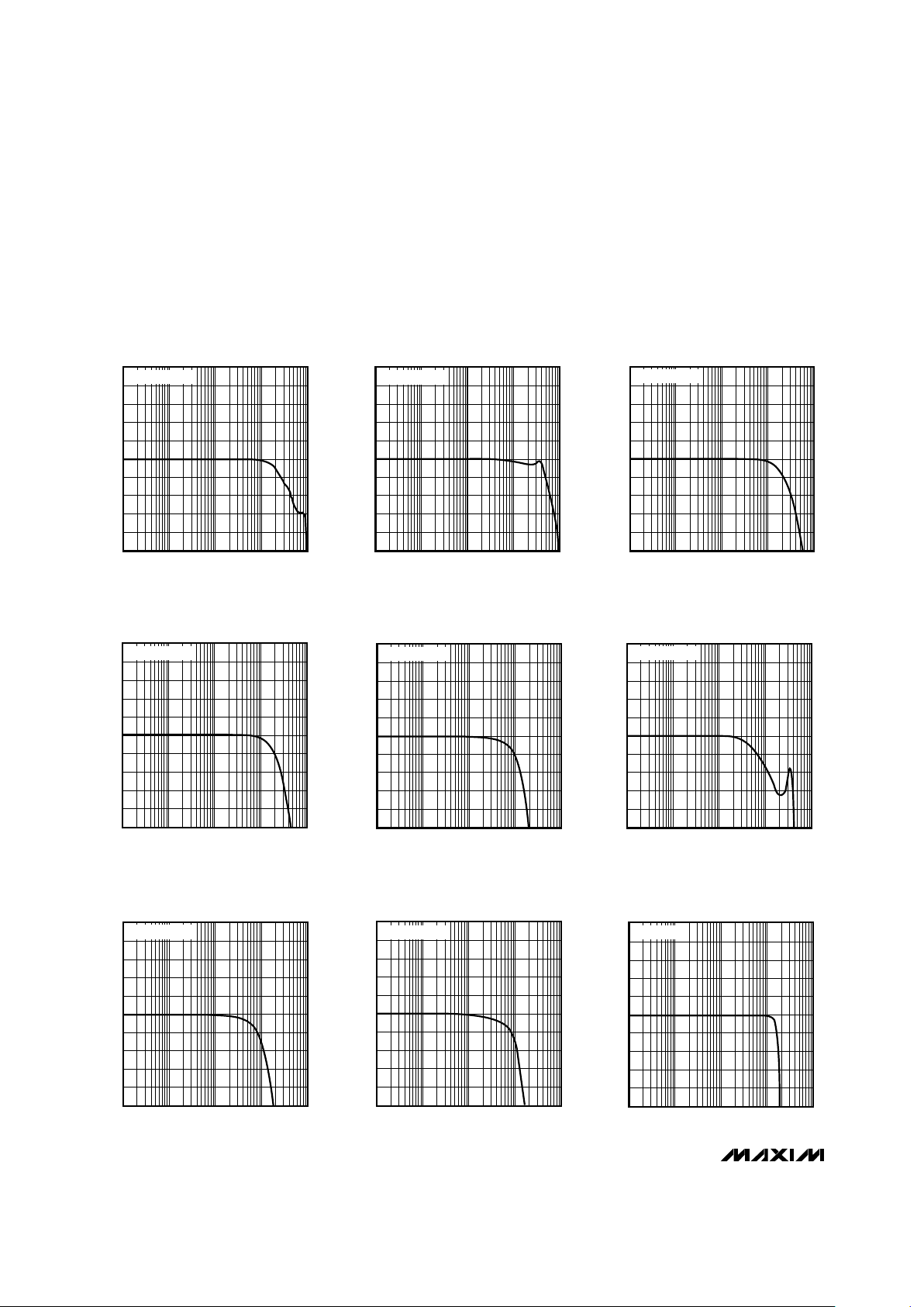
__________________________________________Typical Operating Characteristics
(VCC= +5V, V
EE
= -5V, RF= 330Ω, RL= 100Ω, TA= +25°C, unless otherwise noted.)
5
4
-5
100k 1M 10M 100M 1G
MAX4104
SMALL-SIGNAL GAIN
vs. FREQUENCY (A
VCL
= +1)
-3
-4
FREQUENCY (Hz)
GAIN (dB)
-1
-2
1
0
3
2
MAX4104 TOC01
V
OUT
= 100mVp-p
5
4
-5
100k 1M 10M 100M 1G
MAX4304
SMALL-SIGNAL GAIN
vs. FREQUENCY (A
VCL
= +2)
-3
-4
FREQUENCY (Hz)
NORMALIZED GAIN (dB)
-1
-2
1
0
3
2
MAX4104 TOC 2
V
OUT
= 100mVp-p
5
4
-5
100k 1M 10M 100M 1G
MAX4105
SMALL-SIGNAL GAIN
vs. FREQUENCY (A
VCL
= +5)
-3
-4
FREQUENCY (Hz)
NORMALIZED GAIN (dB)
-1
-2
1
0
3
2
MAX4104 TOC 3
V
OUT
= 100mVp-p
5
4
-5
100k 1M 10M 100M 1G
MAX4305
SMALL-SIGNAL GAIN
vs. FREQUENCY (A
VCL
= +10)
-3
-4
FREQUENCY (Hz)
NORMALIZED GAIN (dB)
-1
-2
1
0
3
2
MAX4104 TOC 4
V
OUT
= 100mVp-p
0.5
0.4
-0.5
100k 1M 10M 100M 1G
MAX4105
GAIN FLATNESS
vs. FREQUENCY (A
VCL
= +5)
-0.3
-0.4
FREQUENCY (Hz)
NORMALIZED GAIN (dB)
-0.1
-0.2
0.1
0
0.3
0.2
MAX4104 TOC 7
V
OUT
= 100mVp-p
0.5
0.4
-0.5
100k 1M 10M 100M 1G
MAX4104
GAIN FLATNESS
vs. FREQUENCY (A
VCL
= +1)
-0.3
-0.4
FREQUENCY (Hz)
GAIN (dB)
-0.1
-0.2
0.1
0
0.3
0.2
MAX4104 TOC 5
V
OUT
= 100mVp-p
0.5
0.4
-0.5
100k 1M 10M 100M 1G
MAX4304
GAIN FLATNESS
vs. FREQUENCY (A
VCL
= +2)
-0.3
-0.4
FREQUENCY (Hz)
NORMALIZED GAIN (dB)
-0.1
-0.2
0.1
0
0.3
0.2
MAX4104 TOC 6
V
OUT
= 100mVp-p
0.5
0.4
-0.5
100k 1M 10M 100M 1G
MAX4305
GAIN FLATNESS
vs. FREQUENCY (A
VCL
= +10)
-0.3
-0.4
FREQUENCY (Hz)
NORMALIZED GAIN (dB)
-0.1
-0.2
0.1
0
0.3
0.2
MAX4104 TOC 8
V
OUT
= 100mVp-p
5
4
-5
100k 1M 10M 100M 1G
MAX4104
LARGE-SIGNAL GAIN
vs. FREQUENCY (A
VCL
= +1)
-3
-4
FREQUENCY (Hz)
GAIN (dB)
-1
-2
1
0
3
2
MAX4104 TOC9
V
OUT
= 2Vp-p
 Loading...