

Page 1
General Description
The MAX4289 micropower, operational amplifier is optimized for ultra-low supply voltage operation. The amplifier consumes only 9µA of quiescent supply current and
is fully specified for operation from a single 1.0V to 5.5V
power supply. This ultra-low voltage operation together
with the low quiescent current consumption make the
MAX4289 ideal for use in battery-powered systems
operated from as little as a single alkaline cell. The
MAX4289 also features a wide input common-mode
range that includes the ground, and an output voltage
swing that is virtually Rail-to-Rail®, allowing almost all of
the power supply to be used for signal voltage.
The low input offset voltage and low input bias current
specifications along with the high open-loop gain make
the MAX4289 well-suited to applications requiring a
high degree of precision.
The MAX4289 is available in a tiny 6-pin SOT23 package. All specifications are guaranteed over the extended temperature range of -40°C to +85°C.
Applications
Features
♦ Ultra-Low Voltage Operation: Guaranteed
Specifications from 1.0V to 5.5V
♦ Input Common-Mode Range: 0 to (VCC- 0.2V)
♦ Ultra-Low Power Consumption: 9µA Supply
Current (typ)
♦ Optimized for Operation from Single-Cell
Battery-Powered Systems
♦ Compatible with 3.0V and 5.0V Single-Supply
Systems
♦ Low Offset Voltage: 0.2mV
♦ Low Input Bias Current: 5nA
♦ High Open-Loop Voltage Gain: 90dB
♦ Rail-to-Rail Output Stage Drives 5kΩ Load
♦ No Output Phase Reversal for Overdriven Inputs
♦ Available in a Tiny 6-Pin SOT23 (3mm
✕
3mm)
MAX4289
1.0V Micropower, SOT23, Operational Amplifier
________________________________________________________________ Maxim Integrated Products 1
Pin Configurations
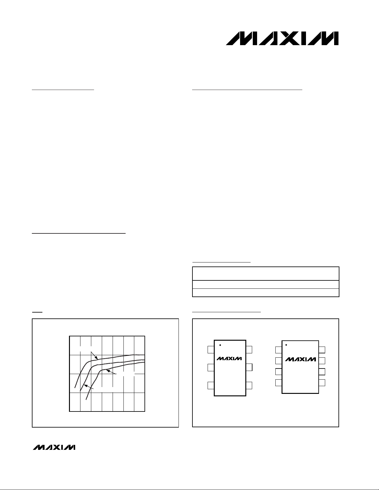
Typical Operating Characteristic
Ordering Information
19-2023; Rev 0; 1/02
For pricing, delivery, and ordering information, please contact Maxim/Dallas Direct! at
1-888-629-4642, or visit Maxim’s website at www.maxim-ic.com.
Single-Cell Systems
Portable Electronic
Equipment
Battery-Powered
Instrumentation
Hearing Aids Using Zinc
Air Battery
Strain Gauges
Cellular Phones
Notebook Computers
Sensor Amplifiers
Portable Communication
Devices
Rail-to-Rail is a registered trademark of Nippon Motorola, Ltd.
PART TEMP RANGE
MAX4289EUT-T -40°C to +85°C 6 SOT23-6 AARX
MAX4289ESA -40°C to +85°C 8 SO —
PINPACKAGE
TOP
MARK
POWER-SUPPLY REJECTION RATIO
90
80
70
PSRR (dB)
60
50
0.8 1.1 1.20.9 1.0 1.3 1.4 1.5
vs. SUPPLY VOLTAGE
TA = +85°C
TA = -40°C
TA = +25°C
SUPPLY VOLTAGE (V)
TOP VIEW
16V
OUT
MAX4289
2
GND
34
SOT23-6
1
N.C.
CC
2
IN-
N.C.
5
IN+
IN-IN+
MAX4289
3
4
SO-8
87N.C.
V
OUT
6
N.C.GND
5
CC
Page 2
MAX4289
1.0V Micropower, SOT23, Operational Amplifier
2 _______________________________________________________________________________________
ABSOLUTE MAXIMUM RATINGS
ELECTRICAL CHARACTERISTICS
(VCC= 3V, VCM= 0, V
OUT
= VCC/2, RLtied to VCC/2, TA= T
MIN
to T
MAX
, unless otherwise noted. Typical values are at TA = +25°C.)
(Note 1)
Stresses beyond those listed under “Absolute Maximum Ratings” may cause permanent damage to the device. These are stress ratings only, and functional
operation of the device at these or any other conditions beyond those indicated in the operational sections of the specifications is not implied. Exposure to
absolute maximum rating conditions for extended periods may affect device reliability.
Power-Supply Voltage (VCCto GND).......................................6V
Input Voltage (IN+ or IN-)...........................(V
CC
+ 0.3V) to -0.3V
Input Current (IN+ or IN-)....................................................20mA
Output Short-Circuit Duration to V
CC
or GND............Continuous
Continuous Power Dissipation (T
A
= +70°C)
6-Pin SOT23 (derate 8.7mW/°C above +70°C).............696mW
8-Pin SO (derate 5.88mW/°C above +70°C).................471mW
Operating Temperature Range ...........................-40°C to +85°C
Junction Temperature......................................................+150°C
Storage Temperature Range .............................-65°C to +150°C
Lead Temperature (soldering, 10s) .................................+300°C
PARAMETER SYMBOL CONDITIONS MIN TYP MAX UNITS
Supply Voltage Range V
Quiescent Supply Current I
Input Offset Voltage V
Input Bias Current I
Input Offset Current I
Differential Input Resistance R
Input Common-Mode Voltage
Range
Power-Supply Rejection Ratio PSRR
Large-Signal Voltage Gain A
Output Voltage Swing High V
Output Voltage Swing Low V
CC
Inferred from the
PSRR tests
V
CC
V
V
OS
OS
V
CM
TA = +25°C ±0.2 ±2.0
TA = T
B
IN
Inferred from
CMRR test
VCC = 1.2V, 0 ≤ VCC - 0.2V 57
VCC = 1.2V, 0 ≤ VCM ≤ VCC - 0.8V 57 85Common-Mode Rejection Ratio CMRR
V
1.0V ≤ VCC ≤ 5.5V, T
1.2V ≤ V
VOL
OH
OL
R
R
Specified as
|V
Specified as V
= 1.0V, T
CC
= 3.0V 12 25
CC
= 5.5V 18 40
CC
to T
MIN
= 3.0V, 0 ≤ VCM ≤ VCC - 0.8V 57 110
CC
≤ 5.5V, T
CC
= 100kΩ (50mV ≤ V
L
= 5kΩ (100mV ≤ V
L
- VOH|
CC
T
= +25°C 1.0 5.5
A
T
= -40°C to +85°C 1.2 5.5
A
= +25°C914
A
MAX
±6.0
±5 ±15 nA
±0.5 ±2.0 nA
50 MΩ
VCC = 1.2V 0 VCC - 0.2
= 3.0V 0 VCC - 0.8
V
CC
= +25°C5475
A
= -40°C to +85°C5875
A
≤ V
OUT
OUT
≤ V
- 50mV) 110
CC
- 100mV) 80 90
CC
RL = 100kΩ 0.2 10
R
= 5kΩ 740
L
OL
RL = 100kΩ 0.4 10
RL = 5kΩ 740
V
µA
mV
V
dB
dB
dB
mV
mV
Page 3
MAX4289
1.0V Micropower, SOT23, Operational Amplifier
_______________________________________________________________________________________ 3
ELECTRICAL CHARACTERISTICS (continued)
(VCC= 3V, VCM= 0, V
OUT
= VCC/2, RLtied to VCC/2, TA= T
MIN
to T
MAX
, unless otherwise noted. Typical values are at TA = +25°C.)
(Note 1)
Note 1: All specifications are 100% production tested at TA= +25°C. Temperature specification limits are guaranteed by design.
Typical Operating Characteristics
(VCC= 3V, VCM= 0, RLto VCC/2, TA= +25°C, unless otherwise noted.)
SUPPLY CURRENT vs. TEMPERATURE
MAX4289 toc01
0
2
6
4
12
14
10
8
16
SUPPLY CURRENT (µA)
-40 0 20-20
40
60 80 100
TEMPERATURE (°C)
VCC = 3V
VCC = 1V
-0.8
-0.6
-0.4
-0.2
0
0.2
0.4
0.6
0.8
0 1.00.5 1.5 2.0 2.5 3.0
INPUT OFFSET VOLTAGE
vs. INPUT COMMON-MODE VOLTAGE
MAX4289 toc02
INPUT COMMON-MODE VOLTAGE (V)
INPUT OFFSET VOLTAGE (mV)
INPUT OFFSET VOLTAGE
vs. TEMPERATURE
MAX4289 toc03
-0.8
-0.6
-0.2
-0.4
0.4
0.6
0.2
0
0.8
INPUT OFFSET VOLTAGE (mV)
-40 0 20-20
40
60 80 100
TEMPERATURE (°C)
PARAMETER SYMBOL CONDITIONS MIN TYP MAX UNITS
Output Short-Circuit Current I
Power-Up Time t
Input Capacitance C
Gain-Bandwidth Product GBW 17 kHz
Phase Margin θM80d egr ees
Gain Margin GM 10 dB
Slew Rate SR 6 V/ms
Capacitive-Load Stability A
Settling Time to 0.1% t
IN
S
Sourcing/sinking
current
A
OUT
PU
VCC = 1.0V 0.6
= 3.0V 19
V
CC
300 µs
3.0 pF
= +1V/V, no sustained oscillations 200 pF
VCL
= +1V/V, no sustained oscillations 75 µs
VCL
mA
Page 4

MAX4289
1.0V Micropower, SOT23, Operational Amplifier
4 _______________________________________________________________________________________
Typical Operating Characteristics (continued)
(VCC= 3V, VCM= 0, RLto VCC/2, TA= +25°C, unless otherwise noted.)
4
6
5
8
7
9
10
-40 20 40-20 0 60 80 100
INPUT BIAS CURENT
vs. TEMPERATURE
MAX4289 toc04
TEMPERATURE (°C)
INPUT BIAS CURRENT (nA)
30
20
10
0
-10
0 1.50.5 1.0 2.0 2.5 3.0
INPUT BIAS CURRENT
vs. INPUT COMMON-MODE VOLTAGE
MAX4289 toc05
INPUT COMMON-MODE VOLTAGE (V)
INPUT BIAS CURRENT (nA)
0
6
4
2
10
8
18
16
14
12
20
-40 -20 0 20 40 60 80 100
OUTPUT SWING HIGH
vs. TEMPERATURE
MAX4289 toc06
TEMPERATURE (°C)
V
OH
(mV)
RL CONNECTED TO GND
RL = 5kΩ
RL = 100kΩ
0
6
4
2
10
8
18
16
14
12
20
-40 -20 0 20 40 60 80 100
OUTPUT SWING LOW
vs. TEMPERATURE
MAX4289 toc07
TEMPERATURE (°C)
V
OL
(mV)
RL CONNECTED TO V
CC
RL = 5kΩ
RL = 100kΩ
30
50
90
70
110
130
0 10050 150 200 250 300
OPEN-LOOP GAIN
vs. OUTPUT SWING LOW
MAX4289 toc08
V
OUT
FROM GND (mV)
GAIN (dB)
RL = 5kΩ
RL = 100kΩ
30
50
90
70
110
130
0 10050 150 200 250 300
OPEN-LOOP GAIN
vs. OUTPUT SWING HIGH
MAX4289 toc09
V
OUT
FROM VCC (mV)
GAIN (dB)
RL = 5kΩ
RL = 100kΩ
60
80
70
100
90
110
120
-40 20 40-20 0 60 80 100
OPEN-LOOP GAIN vs. TEMPERATURE
MAX4289 toc10
TEMPERATURE (°C)
GAIN (dB)
RL = 5kΩ
RL = 100kΩ
RL CONNECTED TO GND
60
80
70
100
90
110
120
-40 20 40-20 0 60 80 100
OPEN-LOOP GAIN vs. TEMPERATURE
MAX4289 toc11
TEMPERATURE (°C)
GAIN (dB)
RL = 5kΩ
RL = 100kΩ
RL CONNECTED TO V
CC
80
-20
0.01 0.1 1 10 100
GAIN AND PHASE vs. FREQUENCY
(C
L
= 0)
0
MAX4289 toc12
FREQUENCY (kHz)
GAIN (dB)
20
40
60
50
30
10
-10
70
180
-20
20
60
100
140
120
80
40
0
160
PHASE (DEGREES)
GAIN
PHASE
Page 5

MAX4289
1.0V Micropower, SOT23, Operational Amplifier
_______________________________________________________________________________________ 5
Typical Operating Characteristics (continued)
(VCC= 3V, VCM= 0, RLto VCC/2, TA= +25°C, unless otherwise noted.)
SMALL-SIGNAL TRANSIENT RESPONSE
IN
50mV/div
OUT
50mV/div
10µs/div
OUTPUT SINKING CURRENT
1.5
VCC = 1V
SINKING CURRENT
1.2
0.9
MAX4289 toc13
vs. OUTPUT VOLTAGE
LARGE-SIGNAL TRANSIENT RESPONSE
IN
1V/div
OUT
1V/div
200µs/div
MAX4289 toc16
MAX4289 toc14
25
20
15
MINIMUM-OPERATING VOLTAGE
vs. TEMPERATURE
1.2
PSRR > 70dB
1.1
(V)
1.0
CC
V
0.9
0.8
-40 20 40-20 0 60 80 100
TEMPERATURE (°C)
OUTPUT SINKING CURRENT
vs. OUTPUT VOLTAGE
VCC = 3V
SINKING CURRENT
MAX4289 toc15
MAX4289 toc17
0.6
OUTPUT CURRENT (mA)
0.3
0
0 0.40.2 0.6 0.8 1.0
OUTPUT VOLTAGE (V)
OUTPUT SOURCING CURRENT
vs. OUTPUT VOLTAGE
1.0
VCC = 1V
SOURCING CURRENT
0.8
0.6
0.4
OUTPUT CURRENT (mA)
0.2
0
0 0.40.2 0.6 0.8 1.0
OUTPUT VOLTAGE (V)
MAX4289 toc18
10
OUTPUT CURRENT (mA)
5
0
0 1.00.5 1.5 2.0 2.5 3.0
OUTPUT VOLTAGE (V)
OUTPUT SOURCING CURRENT
vs. OUTPUT VOLTAGE
25
VCC = 3V
SOURCING CURRENT
20
15
10
OUTPUT CURRENT (mA)
5
0
0 1.00.5 1.5 2.0 2.5 3.0
OUTPUT VOLTAGE (V)
MAX4289 toc19
Page 6

MAX4289
Detailed Description
The MAX4289 consumes ultra-low power (9µA supply
current typically) and has a rail-to-rail output stage that
is specifically designed for low-voltage operation. The
input common-mode voltage range extends from VCC-
0.2V to ground, although full rail-to-rail input range is
possible with degraded performance. The input offset
voltage is typically 200µV. Low-operating supply voltage, low supply current, and rail-to-rail outputs make
this operational amplifier an excellent choice for precision or general-purpose, low-voltage, battery-powered
systems.
Rail-to-Rail Output Stage
The MAX4289 output stage can drive a 5kΩ load and
still swing to within 7mV of the rails. Figure 1 shows the
output voltage swing of the MAX4289 configured as a
unity-gain buffer, powered from a single 2V supply voltage. The output for this setup typically swings from
+0.4mV to (VCC- 0.2mV) with a 100kΩ load.
Applications Information
Power-Supply Considerations
The MAX4289 operates from a single 1.0V to 5.5V supply
and consumes only 9µA of supply current. A high powersupply rejection ratio of 75dB allows the amplifier to be
powered directly off a decaying battery voltage, simplifying design and extending battery life. The MAX4289 is
ideally suited for single-cell battery-powered systems.
Figures 2 and 3 show the supply current and PSRR as a
function of supply voltage and temperature.
1.0V Micropower, SOT23, Operational Amplifier
6 _______________________________________________________________________________________
Pin Description
Figure 1. Rail-to-Rail Input/Output Voltage Range
Figure 2. ICCvs. VCCOver the Temperature Range
SO SOT23
1, 5, 8 5 N.C. No Connection. Not internally connected.
2 4 IN- Inverting Input
3 3 IN+ Noninverting Input
4 2 GND Ground
6 1 OUT Amplifier Output
76V
PIN
NAME FUNCTION
CC
Positive Supply. Bypass with a 0.1µF capacitor to GND.
IN
500mV/div
OUT
VIN = 2.0V
= 1kHz
f
IN
= 100kΩ
R
L
200µs/div
SUPPLY CURRENT
vs. SUPPLY VOLTAGE
25
500mV/div
20
15
TA = +25°C
10
SUPPLY CURRENT (µA)
5
TA = +85°C
TA = -40°C
0
021 3456
SUPPLY VOLTAGE (V)
Page 7

Power-Up Settling Time
The MAX4289 typically requires 300µs to power-up
after VCCis stable. During this startup time, the output
is indeterminate. The application circuit should allow for
this initial delay.
Driving Capacitive Loads
The MAX4289 is unity-gain stable for loads up to
200pF. Applications that require greater capacitivedrive capability should use an isolation resistor
between the output and the capacitive load (Figure 4).
Note that this solution results in a loss of gain accuracy
because R
ISO
forms a voltage-divider with the load
resistor.
Using the MAX4289 as a Comparator
Although optimized for use as an operational amplifier,
the MAX4289 can also be used as a rail-to-rail I/O comparator (Figure 5). External hysteresis can be used to
minimize the risk of output oscillation. The positive feedback circuit, shown in Figure 5, causes the input threshold to change when the output voltage changes state.
Power Supplies and Layout
The MAX4289 operates from a single 1V to 5.5V power
supply. Bypass the power with a 0.1µF capacitor to
ground.
Good layout techniques optimize performance by
decreasing the amount of stray capacitance at the op
amp’s inputs and outputs. To decrease stray capacitance, minimize trace lengths by placing external components close to the op amp’s pins.
MAX4289
1.0V Micropower, SOT23, Operational Amplifier
_______________________________________________________________________________________ 7
Figure 3. PSRR vs. VCCOver the Temperature Range
Figure 4. Using a Resistor to Isolate a Capacitive Load from
the Op Amp
POWER-SUPPLY REJECTION RATIO
vs. SUPPLY VOLTAGE
90
TA = +85°C
80
70
PSRR (dB)
60
50
0.8 1.1 1.20.9 1.0 1.3 1.4 1.5
TA = +25°C
SUPPLY VOLTAGE (V)
TA = -40°C
MAX4289
R
ISO
R
R
R
C
L
+ R
L
ISO
L
AV = ≈ 1
L
Page 8

MAX4289
1.0V Micropower, SOT23, Operational Amplifier
8 _______________________________________________________________________________________
Chip Information
TRANSISTOR COUNT: 557
Figure 5. Hysteresis Comparator Circuit
INPUT
V
OH
OUTPUT
V
HI
V
LO
V
IN
R1
R2
V
EE
R
HYST
V
MAX4289
V
CC
EE
HYSTERESIS
V
OH
V
OL
V
OUT
Page 9

MAX4289
1.0V Micropower, SOT23, Operational Amplifier
Maxim cannot assume responsibility for use of any circuitry other than circuitry entirely embodied in a Maxim product. No circuit patent licenses are
implied. Maxim reserves the right to change the circuitry and specifications without notice at any time.
Maxim Integrated Products, 120 San Gabriel Drive, Sunnyvale, CA 94086 408-737-7600 _____________________ 9
© 2002 Maxim Integrated Products Printed USA is a registered trademark of Maxim Integrated Products.
Package Information
6LSOT.EPS
SOICN.EPS
 Loading...