Maxim MAX4278MJA, MAX4278EUA, MAX4278ESA, MAX4278EPA, MAX4178EUA Datasheet
...
_______________General Description
The MAX4178/MAX4278 are ±5V, wide-bandwidth, fastsettling, closed-loop buffers featuring high slew rate, high
precision, high output current, low noise, and low differential gain and phase errors. The MAX4178, with a -3dB
bandwidth of 330MHz, is preset for unity voltage gain
(0dB). The MAX4278 is preset for a voltage gain of +2
(6dB) and has a 310MHz -3dB bandwidth.
The MAX4178/MAX4278 feature the high slew rate and
low power that are characteristic of current-mode feedback amplifiers. However, unlike conventional currentmode feedback amplifiers, these devices have a
unique input stage that combines the benefits of current-feedback topology with those of the traditional voltage-feedback topology. This combination results in low
input offset voltage and bias current, low noise, and
high gain precision and power-supply rejection.
The MAX4178/MAX4278 are ideally suited for driving
50Ω or 75Ω loads. They are the perfect choice for highspeed cable-driving applications, such as video routing.
The MAX4178/MAX4278 are available in DIP, SO, and
space-saving µMAX and SOT23 packages.
________________________Applications
Broadcast and High-Definition TV Systems
Video Switching and Routing
High-Speed Cable Drivers
Communications
Medical Imaging
Precision High-Speed DAC/ADC Buffers
____________________________Features
♦ High Speed:
330MHz -3dB Bandwidth (MAX4178)
310MHz -3dB Bandwidth (MAX4278)
250MHz Full-Power Bandwidth (V
OUT
= 2Vp-p)
150MHz 0.1dB Flatness Bandwidth
1300V/µs Slew Rate (MAX4178)
1600V/µs Slew Rate (MAX4278)
♦ Low Differential Phase/Gain Error: 0.01°/0.04%
♦ 8mA Supply Current
♦ 1µA Input Bias Current
♦ 0.5mV Input Offset Voltage
♦ 5nV/
√
HHzz
Input-Referred Voltage Noise
♦ 2pA/
√
HHzz
Input-Referred Current Noise
♦ 1.0% Max Gain Error with 100Ω Load
♦ Short-Circuit Protected
♦ 8000V ESD Protection
♦ Available in Space-Saving SOT23 Package
MAX4178/MAX4278
330MHz, Gain of +1/Gain of +2
Closed-Loop Buffers
________________________________________________________________
Maxim Integrated Products
1
19-0468; Rev 1; 5/97
PART
MAX4178EPA
MAX4178ESA
MAX4178EUA -40°C to +85°C
-40°C to +85°C
-40°C to +85°C
TEMP. RANGE
PINPACKAGE
8 Plastic DIP
8 SO
8 µMAX
EVALUATION KIT MANUAL
FOLLOWS DATA SHEET
______________Ordering Information
Ordering Information continued at end of data sheet.
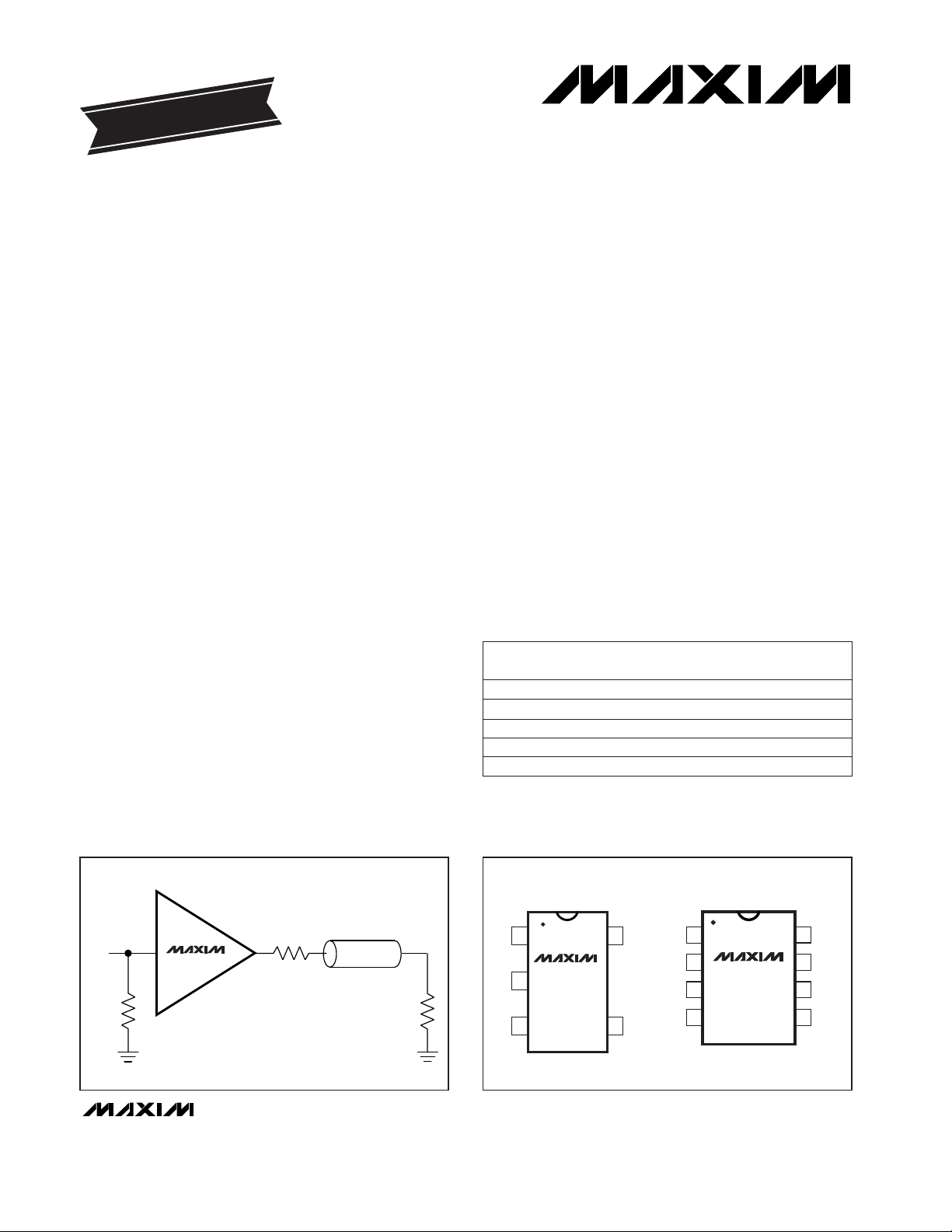
DIP/SO/µMAX
TOP VIEW
OUT
IN
N.C.
V
EE
1
2
8
7
N.C.
V
CC
GND
N.C.
MAX4178
MAX4278
3
4
6
5
V
EE
GNDIN
15V
CC
OUT
SOT23-5
2
34
MAX4178
MAX4278
MAX4278
V
IN
75Ω
75Ω
V
OUT
75Ω
VIDEO/RF CABLE DRIVER
_________________Pin Configurations
__________Typical Operating Circuit
MAX4178MJA -55°C to +125°C 8 CERDIP
MAX4178EUK-T -40°C to +85°C 5 SOT23
SOT
TOP MARK
–
–
–
–
ABYX
For free samples & the latest literature: http://www.maxim-ic.com, or phone 1-800-998-8800.
For small orders, phone 408-737-7600 ext. 3468.

MAX4178/MAX4278
330MHz, Gain of +1/Gain of +2
Closed-Loop Buffers
2 _______________________________________________________________________________________
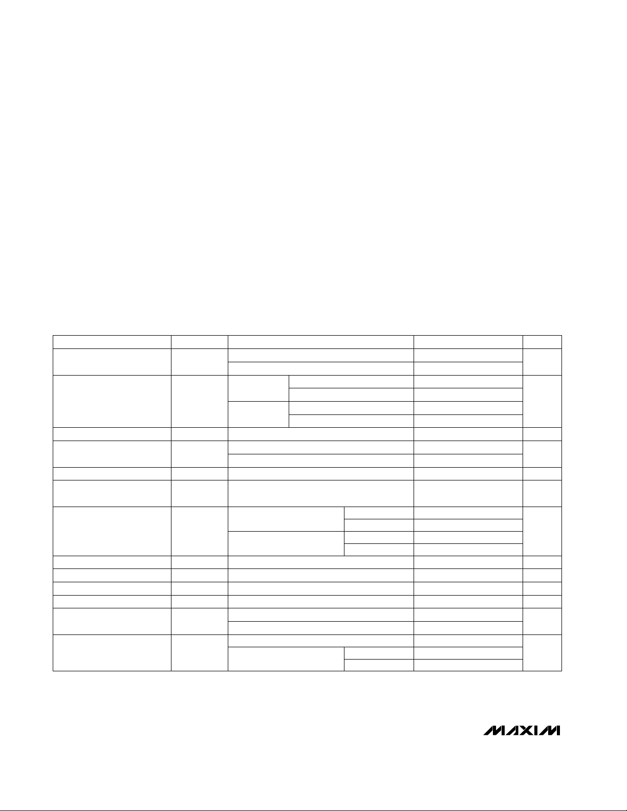
ABSOLUTE MAXIMUM RATINGS
DC ELECTRICAL CHARACTERISTICS
(VCC= +5V, VEE= -5V, V
OUT
= 0V, RL= ∞, TA= T
MIN
to T
MAX
, unless otherwise noted. Typical values are at TA= +25°C.)
Stresses beyond those listed under “Absolute Maximum Ratings” may cause permanent damage to the device. These are stress ratings only, and functional
operation of the device at these or any other conditions beyond those indicated in the operational sections of the specifications is not implied. Exposure to
absolute maximum rating conditions for extended periods may affect device reliability.
Supply Voltage (VCCto VEE)..................................................12V
Input Voltage....................................(V
CC
+ 0.3V) to (VEE- 0.3V)
Output Short-Circuit Duration (to GND) .....................Continuous
Continuous Power Dissipation (T
A
= +70°C)
Plastic DIP (derate 9.09mW/°C above +70°C) ...........727mW
SO (derate 5.88mW/°C above +70°C)........................471mW
µMAX (derate 4.10mW/°C above +70°C) ...................330mW
CERDIP (derate 8.00mW/°C above +70°C)................640mW
SOT23 (derate 7.10mW/°C above +70°C)..................571mW
Operating Temperature Ranges (Note 1)
MAX4178E_A/MAX4278E_A...........................-40°C to +85°C
MAX4178EUK/MAX4278EUK .........................-40°C to +85°C
MAX4178MJA/MAX4278MJA .......................-55°C to +125°C
Storage Temperature Range.............................-65°C to +160°C
Lead Temperature (soldering, 10sec).............................+300°C
CONDITIONS
UNITSMIN TYP MAXSYMBOLPARAMETER
MAX4178 ±2.5 ±3.0
MAX4278
V
±1.25 ±1.5
V
IN
Input Voltage Range
0.5 2.0
µV/°C2TCV
OS
Input Offset Voltage Drift
1 3
µAI
B
Input Bias Current
MΩ1R
IN
Input Resistance
VS= ±4.5V to ±5.5V dB70 90PSRR
Power-Supply Rejection
Ratio
0.990 1.000
MAX4178 (Note 2)
0.985 1.000
1.98 2.01
MAX4278 (Note 3)
V/V
1.97 2.01
A
V
Voltage Gain
V
OUT
= ±1mV to ±2V %0.01A
V(LIN)
Gain Linearity
f = DC Ω0.1R
OUT
Output Resistance
Short to GND mA150I
SC
Short-Circuit Output Current
RL= 100Ω ±2.5 ±3.0
TA = +25°C
RL= 100Ω
RL= 50Ω
RL= 100Ω
RL= 50Ω
RL= 50Ω
V
±2.0 ±2.5
V
OUT
Output Voltage Swing
TA= +25°C 8 10
12
mA
14
TA = T
MIN
to T
MAX
I
SY
Quiescent Supply Current
MAX4_78E_ _
MAX4_78MJA
TA = -40°C to +85°C mA70 100I
OUT
Minimum Output Current
3.0
TA = T
MIN
to T
MAX
5
Note 2: Voltage Gain = (V
OUT
- VOS) / VINmeasured at VIN= ±2.5V.
Note 3: Voltage Gain = (V
OUT
- VOS) / VINmeasured at VIN= ±1.25V.
TA = +25°C
0.5 3.0
TA =
T
MIN
to T
MAX
5.0
mVV
OS
Input Offset Voltage
MAX4_78ESA/EPA/EUA/MJA
MAX4_78EUK
MAX4_78ESA/EPA/EUA/MJA
MAX4_78EUK
Note 1: Specifications for the MAX4_78EUK(SOT23 packages) are 100% tested at TA= +25°C, and guaranteed by design over
temperature.

MHz
MAX4178/MAX4278
330MHz, Gain of +1/Gain of +2
Closed-Loop Buffers
_______________________________________________________________________________________ 3
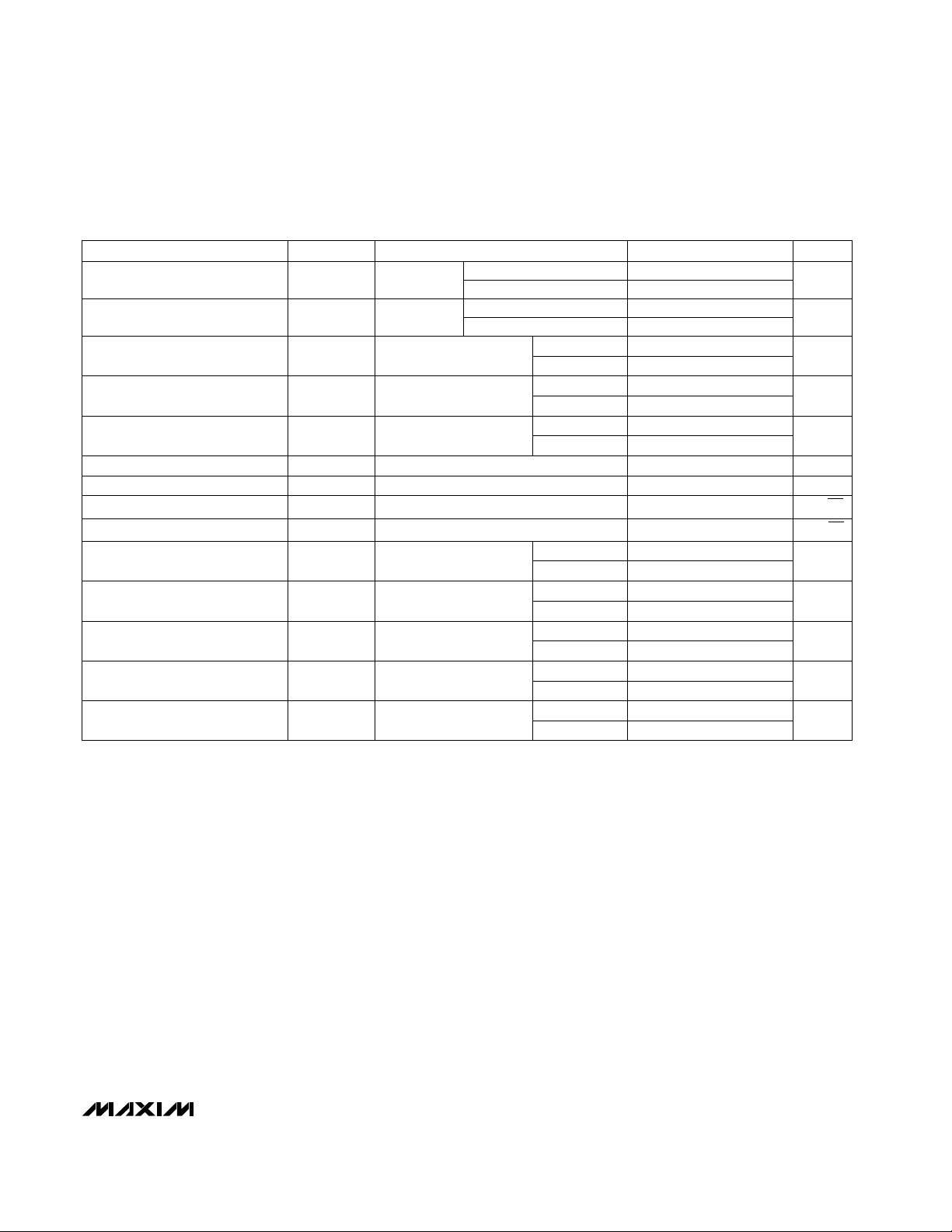
AC ELECTRICAL CHARACTERISTICS
(VCC= +5V, VEE= -5V, RL= 100Ω, TA= +25°C, unless otherwise noted.)
Note 4: Minimum AC specifications are guaranteed by sample test on the MAX4_78ESA only.
Note 5: Tested with a 3.58MHz video test signal with an amplitude of 40IRE superimposed on a linear ramp (0 to 100IRE). An IRE is
a unit of video signal amplitude developed by the Institute of Radio Engineers. 140IRE = 1V in color systems.
240 330
230 310
CONDITIONS
V
OUT
= 2V step ns2tR, t
F
Rise/Fall Times
f = 10MHz nV/√Hz5e
n
Input Voltage Noise Density
f = 10MHz pA/√Hz2i
n
Input Current Noise Density
0.04
f = 3.58MHz %
0.04
DG
Differential Gain
(Note 5)
f = 5MHz, V
OUT
= 2Vp-p dBC
-81
SFDRSpurious-Free Dynamic Range
36
fC= 10MHz,
V
OUT
= 2Vp-p
dBm
31
IP3Third-Order Intercept
UNITSMIN TYP MAXPARAMETER
MAX4278
30 150MAX4178
MAX4278
250
V
OUT
= 2Vp-p MHz
250
FPBWFull-Power Bandwidth
MAX4178
to 0.01%
10
V
OUT
= 2V step ns
12
t
S
Settling Time
to 0.1%
MAX4178
MAX4278
0.01
MAX4278
MAX4178
f = 3.58MHz degrees
0.01
DP
Differential Phase
(Note 5)
-58
MAX4278
MAX4178
fC= 10MHz,
V
OUT
= 2Vp-p
dB
-59
THDTotal Harmonic Distortion
MAX4178
MAX4278
pF1C
IN
Input Capacitance
MAX4178
MAX4278 -74
MAX4178
MAX4278
30 150
SYMBOL
800 1300MAX4178
900 1600MAX4278
V/µsV
OUT
= ±2Vp-pSR
Slew Rate
(Note 4)
MHz
V
OUT
≤
0.1Vp-p
BW
Small-Signal, -3dB Bandwidth
(Note 4)
MHz
V
OUT
≤
0.1Vp-p
BW
(0.1dB)
Small-Signal, ±0.1dB Bandwidth
(Note 4)

MAX4178/MAX4278
330MHz, Gain of +1/Gain of +2
Closed-Loop Buffers
4 _______________________________________________________________________________________
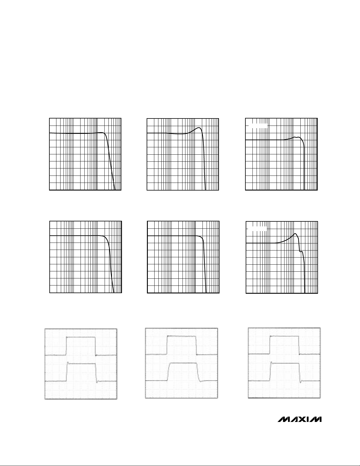
__________________________________________Typical Operating Characteristics
(VCC= +5V, VEE= -5V, RL= 100Ω, CL= 0pF, TA = +25°C, unless otherwise noted.)
2
-8
1M
10M
100M
1G
MAX4178
SMALL-SIGNAL GAIN vs. FREQUENCY
-5
-6
-7
0
-1
-2
-3
-4
1
MAX4178/4278-01
FREQUENCY (Hz)
GAIN (dB)
-0.7
1M
10M
100M
1G
MAX4178
GAIN FLATNESS vs. FREQUENCY
-0.4
-0.5
-0.6
-0.8
0.1
0
-0.1
-0.2
-0.3
0.2
MAX4178/4278-02
FREQUENCY (Hz)
GAIN (dB)
-6
1M
10M
100M
1G
MAX4178
LARGE-SIGNAL GAIN vs. FREQUENCY
-3
-4
-5
-7
2
1
0
-1
-2
3
MAX4178/4278-03
FREQUENCY (Hz)
GAIN (dB)
VO = 2Vp-p
-1
1M
10M
100M
1G
MAX4278
SMALL-SIGNAL GAIN vs. FREQUENCY
2
1
0
-2
7
6
5
4
3
8
MAX4178/4278-04
FREQUENCY (Hz)
GAIN (dB)
5.3
1M
10M
100M
1G
MAX4278
GAIN FLATNESS vs. FREQUENCY
5.6
5.5
5.4
5.2
6.1
6.0
5.9
5.8
5.7
6.2
MAX4178/4278-05
FREQUENCY (Hz)
GAIN (dB)
-6
1M
10M
100M
1G
MAX4278
LARGE-SIGNAL GAIN vs. FREQUENCY
0
-2
-4
-8
10
8
6
4
2
12
MAX4178/4278-06
FREQUENCY (Hz)
GAIN (dB)
VO = 2Vp-p
MAX4178 LARGE-SIGNAL
PULSE RESPONSE (C
L
= 0pF)
MAX4178/4278-08
TIME (10ns/div)
VOLTAGE (2V/div)
IN
OUT
GND
GND
MAX4278 SMALL-SIGNAL
PULSE RESPONSE (C
L
= 0pF)
MAX4178/4278-09
TIME (10ns/div)
VOLTAGE
IN
(50mV/
div)
OUT
(100mV/
div)
GND
GND
MAX4178 SMALL-SIGNAL
PULSE RESPONSE (C
L
= 0pF)
MAX4178/4278-07
TIME (10ns/div)
VOLTAGE (100mV/div)
IN
OUT
GND
GND
 Loading...