

For free samples & the latest literature: http://www.maxim-ic.com, or phone 1-800-998-8800.
For small orders, phone 1-800-835-8769.
General Description
The MAX4265–MAX4270 single-supply, voltage-feedback
op amps are capable of driving a 100Ω load while maintaining ultra-low distortion over a wide bandwidth. They
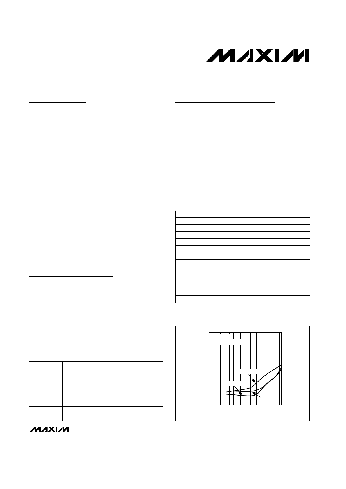
offer superior spurious-free dynamic range (SFDR) performance: -90dBc or better at frequencies below 5MHz and
-60dBc at a 100MHz frequency. Additionally, input voltage
noise density is 8nV/√Hz while operating from a single
+4.5V to +8.0V supply or from dual ±2.25V to ±4.0V supplies. These features make the MAX4265–MAX4270 ideal
for use in high-performance communications and signalprocessing applications that require low distortion and
wide bandwidth.
The MAX4265 single and MAX4268 dual unity-gain-stable
amplifiers have up to a 300MHz gain-bandwidth product.
The MAX4266 single and MAX4269 dual amplifiers have
up to a 350MHz bandwidth at a minimum stable gain of
+2V/V. The MAX4267 single and MAX4270 dual amplifiers
have a 200MHz bandwidth at a minimum stable gain of
+5V/V.
For additional power savings, these amplifiers feature a
low-power disable mode that reduces supply current to
1.6mA and places the outputs in a high-impedance state.
The MAX4265/MAX4266/MAX4267 are available in a
space-saving 8-pin µMAX package, and the MAX4268/
MAX4269/MAX4270 are available in a 16-pin QSOP package.
Applications
Base-Station Amplifiers
IF Amplifiers
High-Frequency ADC Drivers
High-Speed DAC Buffers
RF Telecom Applications
High-Frequency Signal Processing
Features
♦ +4.5V to +8.0V Single-Supply Operation
♦ Superior SFDR with 100Ω Load
-90dBc (f
C
= 5MHz )
-60dBc (f
C
= 100MHz)
♦ 35dBm IP3 (fC= 20MHz)
♦ 8nV/√Hz Voltage Noise Density
♦ 100MHz 0.1dB Gain Flatness (MAX4268)
♦ 900V/µs Slew Rate
♦ ±45mA Output Driving Capability
♦ Shutdown Mode Places Outputs in High-
Impedance State
MAX4265–MAX4270
Ultra-Low-Distortion, Single-Supply,
300MHz Op Amps with Enable
________________________________________________________________ Maxim Integrated Products 1
-20
-100
0.1M 10M 100M
-80
-90
-70
-60
-50
-40
-30
MAX4268/70 toc10
FREQUENCY (Hz)
SFDR (dBc)
1M
V
OUT
= 1Vp-p
MAX4269
MAX4270
MAX4268
RL = 100Ω to VCC/2
19-1552; Rev 0; 10/99
Selector Guide
SFDR vs. Input Frequency
Ordering Information
*Future product—contact factory for availability.
14 SO-40°C to +85°CMAX4270ESD
16 QSOP
14 SO
16 QSOP
14 SO-40°C to +85°C
-40°C to +85°C
-40°C to +85°C
-40°C to +85°C
MAX4270EEE
MAX4269ESD
MAX4269EEE
MAX4268ESD
16 QSOP
8 SO
8 µMAX
8 SO-40°C to +85°C
-40°C to +85°C
-40°C to +85°C
-40°C to +85°C
MAX4268EEE
MAX4267ESA*
MAX4267EUA*
MAX4266ESA*
8 µMAX
PIN-PACKAGETEMP. RANGE
-40°C to +85°C
MAX4266EUA*
PART
200
52MAX4270
35022MAX4269
30012MAX4268
20051MAX4267
35021MAX4266
30011MAX4265
BANDWIDTH
(MHz)
MIN GAIN
(V/V)
NO. OF
OP AMPS
PART
8 SO-40°C to +85°CMAX4265ESA*
8 µMAX-40°C to +85°C
MAX4265EUA*
Pin Configurations appear at end of data sheet.
MAX4265–MAX4270
Ultra-Low-Distortion, Single-Supply,
300MHz Op Amps with Enable
2 _______________________________________________________________________________________
ABSOLUTE MAXIMUM RATINGS
DC ELECTRICAL CHARACTERISTICS
(VCC= +5V, VEE= 0, RL= 100Ω to VCC/2, VCM= VCC/2, TA= T
MIN
to T
MAX
, typical values are at TA= +25°C, unless otherwise noted.)
Stresses beyond those listed under “Absolute Maximum Ratings” may cause permanent damage to the device. These are stress ratings only, and functional
operation of the device at these or any other conditions beyond those indicated in the operational sections of the specifications is not implied. Exposure to
absolute maximum rating conditions for extended periods may affect device reliability.
Supply Voltage (VCCto VEE)...............................................+8.5V
Voltage on Any Other Pin .................(V
EE
- 0.3V) to (VCC+ 0.3V)
Short-Circuit Duration (V
OUT
to VCCor VEE) ..............Continuous
Continuous Power Dissipation (TA= +70°C)
16-Pin QSOP (derate 8.33mW/°C above +70°C)........667mW
8-Pin µMAX (derate 4.10mW/°C above +70°C) ..........330mW
8-Pin SO (derate 5.9mW/°C above +70°C).................471mW
14-Pin SO (derate 8.33mW/°C above +70°C).............667mW
Operating Temperature Range ...........................-40°C to +85°C
Storage Temperature Range .............................-65°C to +150°C
Junction Temperature......................................................+150°C
Lead Temperature (soldering, 10s) .................................+300°C
EN_ Logic Input High Current
130
µAV
EN_
= 5V
PARAMETER SYMBOL MIN TYP MAX UNITS
Input Offset Current I
OS
0.1 5.5
µA
Input Bias Current I
B
3.5 40
µA
Input Offset Voltage Channel
Matching
1
mV
Input Offset Voltage Drift TCV
OS
1.5
µV/°C
Common-Mode Input
Resistance
R
INCM
1
MΩ
Differential Input Resistance R
INDIFF
40
kΩ
Common-Mode Rejection Ratio CMRR
60 85
dB
Power-Supply Rejection Ratio PSRR
60 85
dB
Common-Mode Input Voltage
Operating Supply Voltage
Range
V
CC
4.5 8.0
V
V
CM
VEE+ 1.6 VCC- 1.6
V
Input Offset Voltage V
OS
19
mV
Open-Loop Voltage Gain A
OL
60 95
dB
Output Current Drive I
OUT
±30 ±45
mA
Output Short-Circuit Current I
SC
100
mA
Closed-Loop Output Resistance R
OUT
0.035
Ω
Power-Up Time t
PWRUP
10
µs
Quiescent Supply Current I
S
28 32
1.6 5
Disable Output Leakage Current
0.2 5
µA
EN_ Logic Low Threshold
VCC- 3.5
V
EN_ Logic High Threshold
VCC- 1.5
V
EN_ Logic Input Low Current
5 100
µA
CONDITIONS
1.75V ≤ V
OUT
≤ 3.25V
MAX4268/MAX4269/MAX4270
Either input, (V
EE
+ 1.6) ≤ VCM≤ (VCC- 1.6)
-10mV ≤ VIN≤ 10mV
RL= 20Ω
(VEE+ 1.6V) ≤ VCM≤ (VCC- 1.6V), no load
VCC= 4.5V to 8.0V
Sinking or sourcing to VCCor V
EE
VO= 1V step, 0.1% settling time
Inferred from PSRR test
Normal mode, EN_ = 5V or floating
Inferred from CMRR test
Disable mode, EN_ = 0
V
EN_
= 0, VEE≤ V
OUT
≤ V
CC
V
EN_
= 0
Output Voltage Swing V
OUT
1.1 1.5
dBVCC- VOH, VOL- V
EE
mA
V
OUT
= 1V step
MAX4265–MAX4270
Ultra-Low-Distortion, Single-Supply,
300MHz Op Amps with Enable
_______________________________________________________________________________________ 3
AC ELECTRICAL CHARACTERISTICS
(V
CC
= +5V, VEE= 0, RL= 100Ω to VCC/2, VCM= VCC/2, MAX4265/MAX4268 AV= +1V/V, MAX4266/MAX4269 AV= +2V/V,
MAX4267/MAX4270 A
V
= +5V/V, TA= T
MIN
to T
MAX
, unless otherwise noted. Typical values are at TA= +25°C.)
fC= 100MHz 68
fC= 60MHz 72
Third Harmonic
Distortion
dBc
fC= 20MHz 86
fC= 10MHz 92
fC= 5MHz 95
fC= 1MHz 96
V
OUT
= 1Vp-p
(MAX4269)
fC= 100MHz 60
fC= 60MHz 68
Second Harmonic
Distortion
dBc
fC= 20MHz 78
fC= 10MHz 87
fC= 5MHz 90
fC= 1MHz 88
V
OUT
= 1Vp-p
(MAX4269)
Settling Time (0.1%) tS,
0.1
15 nsV
OUT
= 1V step
Rise/Fall Times tR, t
F
1 nsV
OUT
= 1V step
Slew Rate SR 900 V/µsV
OUT
= 1V step
All-Hostile Crosstalk 85 dBf = 10MHz
MAX4267/MAX4270
MAX4266/MAX4269
MAX4265/MAX4268
0.1dB Gain Flatness BW
0.1dB
100
MHz
35
35
V
OUT
= 100mVp-p
MAX4267/MAX4270
MAX4266/MAX4269
MAX4265/MAX4268
Full-Power Bandwidth FPBW
175
MHz
200
200
V
OUT
= 1Vp-p
fC= 100MHz 60
fC= 60MHz 68
fC= 20MHz 78
fC= 10MHz 87
fC= 5MHz 90
Spurious-Free Dynamic
Range SFDR dBc
fC= 1MHz 88
V
OUT
= 1Vp-p
(MAX4269)
MAX4267/MAX4270
MAX4266/MAX4269
MAX4265/MAX4268
PARAMETER SYMBOL MIN TYP MAX UNITS
Small-Signal -3dB Bandwidth BW
-3dB
300
MHz
350
200
CONDITIONS
V
OUT
= 100mVp-p
4
-6
0.1M 1M 10M 100M 1G
SMALL-SIGNAL BANDWIDTH
-4
MAX4268/70 toc01a
FREQUENCY (Hz)
GAIN (dB)
-2
0
2
1
-1
-3
-5
3
V
OUT
= 100mVp-p
MAX4270
MAX4269
MAX4268
Typical Operating Characteristics
(V
CC
= +5V, VEE= 0, EN_ = 5V, RL= 100Ω to VCC/2, MAX4268 AV= +1V/V, MAX4269 AV= +2V/V, MAX4270 AV= +5V/V, TA=+25°C,
unless otherwise noted.)
MAX4265–MAX4270
Ultra-Low-Distortion, Single-Supply,
300MHz Op Amps with Enable
4 _______________________________________________________________________________________
NTSC, f = 3.58MHz, RL= 150Ω to VCC/2
fC= 20MHz
V
OUT
= 1Vp-p, fCA= 20MHz,
f
CB
= 21.25MHz (MAX4269)
No sustained
oscillation
V
IN
= 1V
f = 10MHz
V
EN_
= 0
f = 1kHz
V
IN
= 1V
f = 1kHz
CONDITIONS
pA/√Hz
1i
n
Input Current Noise Density
nV/√Hz
8e
n
Input Voltage Noise Density
%0.015D
G
Differential Gain
dBm12
dBm35IP3
Two-Tone, Third-Order
Intercept Distortion
Input -1dB Compression Point
22
15
pF
15
Capacitive Load Stability
µs750t
DIS
Disable Time
pF2C
IN
Input Capacitance
Ω1R
OUT
Output Impedance
pF5Disabled Output Capacitance
ns100t
EN
Enable Time
UNITSMIN TYP MAXSYMBOLPARAMETER
MAX4265/MAX4268
MAX4266/MAX4269
MAX4267/MAX4270
NTSC, f = 3.58MHz, RL= 150Ω to VCC/2 degrees0.03D
P
Differential Phase
AC ELECTRICAL CHARACTERISTICS (continued)
(V
CC
= +5V, VEE= 0, RL= 100Ω to VCC/2, VCM= VCC/2, MAX4265/MAX4268 AV= +1V/V, MAX4266/MAX4269 AV= +2V/V,
MAX4267/MAX4270 A
V
= +5V/V, TA= T
MIN
to T
MAX
, unless otherwise noted. Typical values are at TA= +25°C.)
4
-6
0.1M 1M 10M 100M 1G
LARGE-SIGNAL GAIN
vs. FREQUENCY
-4
MAX4268/70 toc02a
FREQUENCY (Hz)
GAIN (dB)
-2
0
2
1
-1
-3
-5
3
V
OUT
= 1Vp-p
MAX4269
MAX4270
MAX4268
0.4
-0.6
0.1M 1M 10M 100M 1G
GAIN FLATNESS vs. FREQUENCY
-0.4
MAX4268/70 toc3
FREQUENCY (Hz)
GAIN (dB)
-0.2
0
0.2
0.1
-0.1
-0.3
-0.5
0.3
MAX4268
MAX4270
MAX4269
MAX4265–MAX4270
Ultra-Low-Distortion, Single-Supply,
300MHz Op Amps with Enable
_______________________________________________________________________________________ 5
Typical Operating Characteristics (continued)
(V
CC
= +5V, VEE= 0, EN_ = 5V, RL= 100Ω to VCC/2, MAX4268 AV= +1V/V, MAX4269 AV= +2V/V, MAX4270 AV= +5V/V, TA=+25°C,
unless otherwise noted.)
-20
-100
0.1M 10M 100M
MAX4268
DISTORTION vs. FREQUENCY
-80
-90
-70
-60
-50
-40
-30
MAX4268/70 toc04
FREQUENCY (Hz)
DISTORTION (dBc)
1M
2ND HARMONIC
3RD HARMONIC
V
OUT
= 1Vp-p
-20
-100
0.1M 10M 100M
MAX4269
DISTORTION vs. FREQUENCY
-80
-90
-70
-60
-50
-40
-30
MAX4268/70 toc05
FREQUENCY (Hz)
DISTORTION (dBc)
1M
V
OUT
= 1Vp-p
3RD HARMONIC
2ND HARMONIC
-20
-100
0.1M 10M 100M
MAX4270
DISTORTION vs. FREQUENCY
-80
-90
-70
-60
-50
-40
-30
MAX4268/70 toc06
FREQUENCY (Hz)
DISTORTION (dBc)
1M
V
OUT
= 1Vp-p
3RD HARMONIC
2ND HARMONIC
-100
-90
-80
-70
-60
-50
-40
-30
-20
0 200100 300 400 500 600
MAX4268
DISTORTION vs. LOAD
MAX4268/70 toc07
RESISTIVE LOAD (Ω)
DISTORTION (dBc)
fO = 5MHz
V
OUT
= 1Vp-p
3RD HARMONIC
2ND HARMONIC
-100
-90
-80
-70
-60
-50
-40
-30
-20
0 200100 300 400 500 600
MAX4269
DISTORTION vs. LOAD
MAX4268/70 toc08
RESISTIVE LOAD (Ω)
DISTORTION (dBc)
fO = 5MHz
V
OUT
= 1Vp-p
3RD HARMONIC
2ND HARMONIC
-100
-90
-80
-70
-60
-50
-40
-30
-20
0 200100 300 400 500 600
MAX4270
DISTORTION vs. LOAD
MAX4268/70 toc09
RESISTIVE LOAD (Ω)
DISTORTION (dBc)
fO = 5MHz
V
OUT
= 1Vp-p
3RD HARMONIC
2ND HARMONIC
-100
-80
-90
-70
-40
-30
-50
-60
-20
0 0.5 1.0 1.5 2.0 2.5
MAX4268
DISTORTION vs. VOLTAGE SWING
MAX4268/70 toc10
VOLTAGE SWING (Vp-p)
DISTORTION (dBc)
fO = 5MHz
3RD HARMONIC
2ND HARMONIC
-100
-80
-90
-70
-40
-30
-50
-60
-20
0 0.5 1.0 1.5 2.0 2.5
MAX4269
DISTORTION vs. VOLTAGE SWING
MAX4268/70 toc11
VOLTAGE SWING (Vp-p)
DISTORTION (dBc)
fO = 5MHz
3RD HARMONIC
2ND HARMONIC
-100
-80
-90
-70
-40
-30
-50
-60
-20
0 0.5 1.0 1.5 2.0 2.5
MAX4270
DISTORTION vs. VOLTAGE SWING
MAX4268/70 toc12
VOLTAGE SWING (Vp-p)
DISTORTION (dBc)
fO = 5MHz
3RD HARMONIC
2ND HARMONIC

MAX4265–MAX4270
Ultra-Low-Distortion, Single-Supply,
300MHz Op Amps with Enable
6 _______________________________________________________________________________________
Typical Operating Characteristics (continued)
(V
CC
= +5V, VEE= 0, EN_ = 5V, RL= 100Ω to VCC/2, MAX4268 AV= +1V/V, MAX4269 AV= +2V/V, MAX4270 AV= +5V/V, TA=+25°C,
unless otherwise noted.)
0.1
0.001
0.1M 10M 100M
0.01
FREQUENCY (Hz)
THD + NOISE (%)
1M
TOTAL HARMONIC DISTORTION
PLUS NOISE vs. FREQUENCY
V
OUT
= 1Vp-p
MAX4269
MAX4270
MAX4268
MAX4268/70 toc13
-20
-100
0.1M 10M 100M
SPURIOUS-FREE DYNAMIC RANGE
vs. FREQUENCY
-80
-90
-70
-60
-50
-40
-30
MAX4268/70 toc14
FREQUENCY (Hz)
SFDR (dBc)
1M
V
OUT
= 1Vp-p
MAX4269
MAX4270
MAX4268
60
20
0.1M 10M 100M
TWO-TONE THIRD-ORDER
INTERCEPT vs. FREQUENCY
30
25
35
40
45
50
55
MAX4268/70 toc15
FREQUENCY (Hz)
INTERCEPT (dBm)
1M
MAX4269
MAX4270
MAX4268
1 10k 1M100101k 100k 10M
VOLTAGE NOISE vs. FREQUENCY
MAX4268/70 toc16
FREQUENCY (Hz)
1
10
100
VOLTAGE NOISE (nV/√Hz)
1000
100
10
1
0.1
0.01
0.1M 10M 100M1M 1G
OUTPUT IMPEDANCE vs. FREQUENCY
MAX4268/70 toc17
FREQUENCY (Hz)
OUTPUT IMPEDANCE (Ω)
0
-120
0.1M 10M 100M1M 1G
MAX4268/MAX4269/MAX4290
CROSSTALK vs. FREQUENCY
MAX4268/70 toc18
FREQUENCY (Hz)
CROSSTALK (dB)
-100
-80
-60
-40
-20
0.020
0.015
0.010
0.005
0.000
-0.005
MAX4268
DIFFERENTIAL GAIN AND PHASE
MAX4268/70 toc19
DIFF PHASE (°) DIFF GAIN (%)
0.04
0.03
0.02
0.01
0.00
-0.01
IRE 10010
IRE 100
R
L
= 150Ω
10
0.020
0.010
0.000
-0.010
-0.020
-0.030
MAX4269
DIFFERENTIAL GAIN AND PHASE
MAX4268/70 toc20
DIFF PHASE (°) DIFF GAIN (%)
0.012
0.008
0.004
0.000
-0.004
-0.008
IRE 10010
IRE 100
R
L
= 150Ω
10
0.006
0.004
0.002
0.000
-0.002
-0.004
-0.006
MAX4270
DIFFERENTIAL GAIN AND PHASE
MAX4268/70 toc21
DIFF PHASE (°) DIFF GAIN (%)
0.010
0.000
-0.010
-0.020
-0.030
IRE 10010
IRE 100
R
L
= 150Ω
10

MAX4265–MAX4270
Ultra-Low-Distortion, Single-Supply,
300MHz Op Amps with Enable
_______________________________________________________________________________________ 7
Typical Operating Characteristics (continued)
(V
CC
= +5V, VEE= 0, EN_ = 5V, RL= 100Ω to VCC/2, MAX4268 AV= +1V/V, MAX4269 AV= +2V/V, MAX4270 AV= +5V/V, TA=+25°C,
unless otherwise noted.)
0
-100
0.1M 1M 10M 100M 1G
POWER-SUPPLY REJECTION RATIO
vs. FREQUENCY
-80
MAX4268/70 toc22
FREQUENCY (Hz)
PSRR (dB)
-60
-40
-20
-30
-50
-70
-90
-10
0
-90
10k 100k 1M 10M 100M 1G
COMMON-MODE REJECTION RATIO
vs. FREQUENCY
-80
-70
MAX14268/70 toc23
FREQUENCY (Hz)
CMRR (dB)
-50
-60
-20
-10
-30
-40
0
1.0
0.5
2.0
1.5
3.0
2.5
3.5
4.5
4.0
5.0
0 200 400 600 800 1000
OUTPUT VOLTAGE SWING
vs. RESISTIVE LOAD
MAX4268/70 toc24
LOAD (Ω)
OUTPUT VOLTAGE SWING (V)
V
OH
V
OL
V
CC
2.5V/div
OUTPUT
500mV/div
0V
5V
POWER-UP/POWER-DOWN RESPONSE
MAX4268/70 toc25
5µs/div
INPUT TO
SHUTDOWN
OUTPUT
500mV/div
0V
ENABLED
SHUT
DOWN
5V
SHUTDOWN/ENABLE RESPONSE
MAX4268/70 toc26
250ns/div
-1.20
-1.10
-1.15
-1.00
-1.05
-0.95
-0.90
4.5 6.0 6.55.0 5.5 7.0 7.5 8.0
INPUT OFFSET VOLTAGE
vs. SUPPLY VOLTAGE
MAX4268/70 toc27
SUPPLY VOLTAGE (V)
INPUT OFFSET VOLTAGE (mV)
-0
-1.5
-1.0
-0.5
-3.5
-3.0
-2.5
-2.0
-4.0
-4.5
-5.0
4.5 6.0 6.55.0 5.5 7.0 7.5 8.0
INPUT BIAS CURRENT
vs. SUPPLY VOLTAGE
MAX4268/70 toc28
SUPPLY VOLTAGE (V)
INPUT BIAS CURRENT (µA)

MAX4265–MAX4270
Ultra-Low-Distortion, Single-Supply,
300MHz Op Amps with Enable
8 _______________________________________________________________________________________
Typical Operating Characteristics (continued)
(V
CC
= +5V, VEE= 0, EN_ = 5V, RL= 100Ω to VCC/2, MAX4268 AV= +1V/V, MAX4269 AV= +2V/V, MAX4270 AV= +5V/V, TA=+25°C,
unless otherwise noted.)
2
1
0
3
4
5
-50 10 25-20-35 -5 40 55 70 85
INPUT BIAS CURRENT vs. TEMPERATURE
MAX4268/70 toc31
TEMPERATURE (°C)
INPUT BIAS CURRENT (µA)
-500
-200
-300
-400
200
100
0
-100
300
400
500
-50 10 25-20-35 -5 40 55 70 85
INPUT OFFSET CURRENT
vs. TEMPERATURE
MAX4268/70 toc32
TEMPERATURE (°C)
INPUT OFFSET CURRENT (nA)
25
28
27
26
32
31
30
29
33
34
35
-50 10 25-20-35 -5 40 55 70 85
SUPPLY CURRENT (PER AMPLIFIER)
vs. TEMPERATURE
MAX4268/70 toc33
TEMPERATURE (°C)
SUPPLY CURRENT (mA)
0
1
3
2
4
5
-50 10 25-20-35 -5 40 55 70 85
VOLTAGE SWING vs. TEMPERATURE
MAX4268/70 toc34
TEMPERATURE (°C)
VOLTAGE SWING (V)
V
OH
V
OL
25
28
27
26
32
31
30
29
33
34
35
4.5 6.0 6.55.0 5.5 7.0 7.5 8.0
SUPPLY CURRENT (PER AMPLIFIER)
vs. SUPPLY VOLTAGE
MAX4268/70 toc29
SUPPLY VOLTAGE (V)
SUPPLY CURRENT (mA)
-5
-2
-3
-4
2
1
0
-1
3
4
5
-50 10 25-20-35 -5 40 55 70 85
INPUT OFFSET VOLTAGE
vs. TEMPERATURE
MAX4268/70 toc30
TEMPERATURE (°C)
INPUT OFFSET VOLTAGE (mV)

Typical Operating Characteristics (continued)
(V
CC
= +5V, VEE= 0, EN_ = 5V, RL= 100Ω to VCC/2, MAX4268 AV= +1V/V, MAX4269 AV= +2V/V, MAX4270 AV= +5V/V, TA=+25°C,
unless otherwise noted.)
MAX4265–MAX4270
Ultra-Low-Distortion, Single-Supply,
300MHz Op Amps with Enable
_______________________________________________________________________________________ 9
INPUT
50mV/div
OUTPUT
50mV/div
MAX4268
SMALL-SIGNAL PULSE RESPONSE
MAX4268/70 toc35
5ns/div
INPUT
25mV/div
OUTPUT
50mV/div
MAX4269
SMALL-SIGNAL PULSE RESPONSE
MAX4268/70 toc36
5ns/div
INPUT
10mV/div
OUTPUT
50mV/div
MAX4270
SMALL-SIGNAL PULSE RESPONSE
MAX4268/70 toc37
5ns/div
INPUT
500mV/div
OUTPUT
500mV/div
MAX4268
LARGE-SIGNAL PULSE RESPONSE
MAX4268/70 toc38
5ns/div
INPUT
250mV/div
OUTPUT
500mV/div
MAX4269
LARGE-SIGNAL PULSE RESPONSE
MAX4268/70 toc39
5ns/div
INPUT
100mV/div
OUTPUT
500mV/div
MAX4270
LARGE-SIGNAL PULSE RESPONSE
MAX4268/70 toc40
5ns/div

FUNCTION
MAX4265–MAX4270
Ultra-Low-Distortion, Single-Supply,
300MHz Op Amps with Enable
10 ______________________________________________________________________________________
14 SO
1 — EN
— 4, 5 ENA, ENB
8 µMAX/SO
2 — IN-
— 2, 9 INA-, INB-
6 — OUT
4, 5 6, 7 V
EE
— 3, 10 INA+, INB+
3 — IN+
— 11, 12 N.C.
7, 8 13, 14 V
CC
— 1, 8 OUTA, OUTB
Pin Description
16 QSOP
—
4, 5
—
2, 11
—
6, 7
3, 12
—
8, 9, 13, 14
15, 16
1, 10
No Connection. Not internally connected.
Positive Power Supply. Connect to a +4.5V to +8.0V supply and
bypass with a 0.1µF capacitor for single-supply operation.
Amplifier Output
Amplifier Output
Negative Power Supply
Noninverting Input
Noninverting Input
Inverting Input
Inverting Input
Enable Input. Active high. Connect to VCCfor normal operation.
Enable Input. Active high. Connect to VCCfor normal operation.
MAX4268
MAX4269
MAX4270
NAME
MAX4265
MAX4266
MAX4267
PIN
FUNCTION
_______________Detailed Description
The MAX4265–MAX4270 single-supply operational
amplifiers feature ultra-low distortion and wide bandwidth. Their low distortion and low noise make them
ideal for driving high-speed analog-to-digital converters
(ADCs) up to 16 bits in telecommunications applications and high-performance signal processing.
These devices can drive loads as low as 100Ω and
deliver 45mA while maintaining DC accuracy and AC
performance. The input common-mode voltage ranges
from (VEE+ 1.6V) to (VCC- 1.6V), while the output
swings to within 1.1V of the rails.
Low Distortion
The MAX4265–MAX4270 use proprietary bipolar technology to achieve minimum distortion in single-supply
systems—a feature typically available only in dual-supply op amps.
Several factors can affect the noise and distortion that a
device contributes to the input signal. The following
guidelines explain how various design choices impact
the total harmonic distortion (THD).
• Choose the proper feedback-resistor and gain-resistor values for the application. In general, the smaller
the closed-loop gain, the smaller the THD generated—especially when driving heavy resistive loads.
Large-value feedback resistors can significantly
improve distortion. The MAX4265–MAX4270’s THD
normally increases at approximately 20dB per
decade at frequencies above 1MHz; this is a lower
rate than that of comparable dual-supply op amps.
• Operating the device near or above the full-power
bandwidth significantly degrades distortion (see the
Total Harmonic Distortion vs. Frequency graph in the
Typical Operating Characteristics).
• The decompensated devices (MAX4266/MAX4267/
MAX4269/MAX4270) deliver the best distortion performance since they have a slightly higher slew rate
and provide a higher amount of loop gain for a given
closed-loop gain setting.

Choosing Resistor Values
Unity-Gain Configurations
The MAX4265 and MAX4268 are internally compensated for unity gain. When configured for unity gain, they
require a small resistor (RF) in series with the feedback
path (Figure 1). This resistor improves AC response by
reducing the Q of the tank circuit, which is formed by
parasitic feedback inductance and capacitance.
Inverting and Noninverting Configurations
The values of the gain-setting feedback and input resistors are important design considerations. Large resistor
values will increase voltage noise and interact with the
amplifier’s input and PC board capacitance to generate
undesirable poles and zeros, which can decrease
bandwidth or cause oscillations. For example, a noninverting gain of +2V/V (Figure 1) using R
F
= RG= 1kΩ
combined with 2pF of input capacitance and 0.5pF of
board capacitance will cause a feedback pole at
128MHz. If this pole is within the anticipated amplifier
bandwidth, it will jeopardize stability. Reducing the 1kΩ
resistors to 100Ω extends the pole frequency to
1.28GHz, but could limit output swing by adding 200Ω
in parallel with the amplifier’s load. Clearly, the selection of resistor values must be tailored to the specific
application.
Distortion Considerations
The MAX4265–MAX4270 are ultra-low-distortion, highbandwidth op amps. Output distortion will degrade as
the total load resistance seen by the amplifier decreases. To minimize distortion, keep the input and gain-setting resistor values relatively large. A 500Ω feedback
resistor combined with an appropriate input resistor to
set the gain will provide excellent AC performance without significantly increasing distortion.
Noise Considerations
The amplifier’s input-referred noise-voltage density is
dominated by flicker noise at lower frequencies and by
thermal noise at higher frequencies. Because the thermal noise contribution is affected by the parallel combination of the feedback resistive network, those resistor
values should be reduced in cases where the system
bandwidth is large and thermal noise is dominant. This
noise-contribution factor decreases, however, with
increasing gain settings. For example, the input noise
voltage density at the op amp input with a gain of
+10V/V using RF= 100kΩ and RG= 11kΩ is en=
18nV/√Hz. The input noise can be reduced to 8nV/√Hz
by choosing RF= 1kΩ, RG= 110Ω.
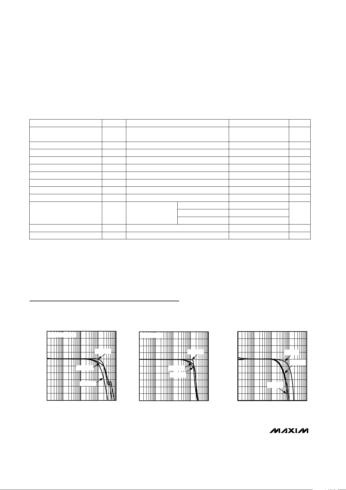
Driving Capacitive Loads
The MAX4265–MAX4270 are not designed to drive
highly reactive loads; stability is maintained with loads
up to 15pF with less than 2dB peaking in the frequency
response. To drive higher capacitive loads, place a
small isolation resistor in series between the amplifier’s
output and the capacitive load (Figure 1). This resistor
improves the amplifier’s phase margin by isolating the
capacitor from the op amp’s output.
To ensure a load capacitance that limits peaking to less
than 2dB, select a resistance value from Figure 2. For
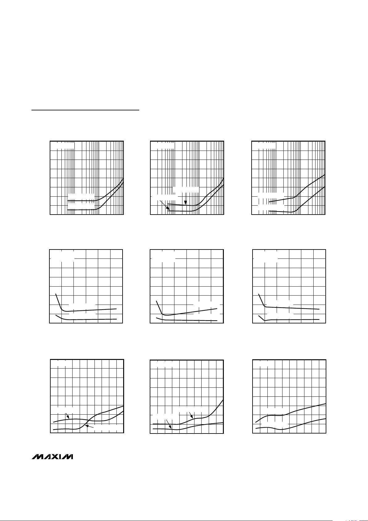
example, if the capacitive load is 100pF, the corresponding isolation resistor is 6Ω (MAX4269). Figures 3
and 4 show the peaking that occurs in the frequency
response with and without an isolation resistor.
Coaxial cable and other transmission lines are easily
driven when terminated at both ends with their characteristic impedance. When driving back-terminated
transmission lines, the capacitive load of the transmission line is essentially eliminated.
ADC Input Buffer
Input buffer amplifiers can be a source of significant
errors in high-speed ADC applications. The input buffer
is usually required to rapidly charge and discharge the
ADC’s input, which is often capacitive (see Driving
Capacitive Loads). In addition, since a high-speed
ADC’s input impedance often changes very rapidly during the conversion cycle, measurement accuracy must
MAX4265–MAX4270
Ultra-Low-Distortion, Single-Supply,
300MHz Op Amps with Enable
______________________________________________________________________________________ 11
R
F
R
G
R
S
*
C
L
V
IN
PART
MAX4265
MAX4266
MAX4267
RF (Ω)
24
500
500
RG (Ω)
∞
500
125
GAIN (V/V)
1
2
5
R
L
*OPTIONAL, USED TO MINIMIZE PEAKING FOR CL > 15pF.
MAX4265
MAX4266
MAX4267
Figure 1. Noninverting Configuration

MAX4265–MAX4270
Ultra-Low-Distortion, Single-Supply,
300MHz Op Amps with Enable
12 ______________________________________________________________________________________
5
-5
0.1M 1M 10M 100M 1G
-3
FREQUENCY (Hz)
GAIN (dB)
-1
1
3
2
0
-2
-4
4
CL = 2.2pF
CL = 5.1pF
CL = 7.3pF
Figure 3a. MAX4268 Small-Signal Gain vs. Frequency
Without Isolation Resistor
5
-5
0.1M 1M 10M 100M 1G
-3
FREQUENCY (Hz)
GAIN (dB)
-1
1
3
2
0
-2
-4
4
CL = 2.2pF
CL = 5.1pF
CL = 7.3pF
Figure 3b. MAX4269 Small-Signal Gain vs. Frequency
Without Isolation Resistor
4
-6
0.1M 1M 10M 100M 1G
-4
FREQUENCY (Hz)
GAIN (dB)
-2
0
2
1
-1
-3
-5
3
CL = 10pF
CL = 15pF
CL = 7.3pF
Figure 3c. MAX4270 Small-Signal Gain vs. Frequency
Without Isolation Resistor
5
-5
0.1M 1M 10M 100M 1G
-3
FREQUENCY (Hz)
GAIN (dB)
-1
1
3
2
0
-2
-4
4
CL = 10pF
R
ISO
= 12Ω
CL = 10pF
R
ISO
= 15Ω
CL = 10pF
R
ISO
= 18Ω
Figure 4a. MAX4268 Small-Signal Gain vs. Frequency
With Isolation Resistor
be maintained using an amplifier with very low output
impedance at high frequencies. The combination of
high speed, fast slew rate, low noise, and a low and
stable distortion over load makes the MAX4265–
MAX4270 ideally suited for use as buffer amplifiers in
high-speed ADC applications.
Low-Power Disable Mode
The MAX4265–MAX4270 feature an active-high enable
pin that can be used to save power and place the outputs in a high-impedance state. Drive EN_ with logic
levels or connect EN_ to VCCfor normal operation. In
the dual versions (MAX4268/MAX4269/MAX4270),
each individual op amp is enabled separately, allowing
the devices to be used in a multiplex configuration. The
supply current in low-power mode is reduced to 1.6mA
per device. Enable time is typically 100ns, and disable
time is typically 750µs.
20
15
10
5
0
06020 40 80 100 120
C
LOAD
(pF)
R
ISO
(Ω)
MAX4268
MAX4269
MAX4270
Figure 2. MAX4268/MAX4269/MAX4270 Isolation Resistance
vs. Capacitive Load

MAX4265–MAX4270
Ultra-Low-Distortion, Single-Supply,
300MHz Op Amps with Enable
______________________________________________________________________________________ 13
5
-5
0.1M 1M 10M 100M 1G
-3
FREQUENCY (Hz)
GAIN (dB)
-1
1
3
2
0
-2
-4
4
CL = 10pF
R
ISO
= 12Ω
CL = 10pF
R
ISO
= 15Ω
CL = 10pF
R
ISO
= 18Ω
Figure 4b. MAX4269 Small-Signal Gain vs. Frequency With
Isolation Resistor
4
-6
0.1M 1M 10M 100M 1G
-4
FREQUENCY (Hz)
GAIN (dB)
-2
0
2
1
-1
-3
-5
3
CL = 22pF
R
ISO
= 22Ω
CL = 22pF
R
ISO
= 3.9Ω
CL = 22pF
R
ISO
= 6Ω
Figure 4c. MAX4270 Small-Signal Gain vs. Frequency With
Isolation Resistor
Power Supplies and Layout
The MAX4265–MAX4270 operate from a single +4.5V
to +8.0V power supply or from dual ±2.25V to ±4.0V
supplies. For single-supply operation, bypass each
power-supply input with a 0.1µF ceramic capacitor
placed close to the VCCpins, and an additional 10µF to
VEE. When operating from dual supplies, bypass each
supply to ground.
Good layout improves performance by decreasing the
amount of stray capacitance and noise at the op amp’s
inputs and output. To decrease stray capacitance, minimize PC board trace lengths and resistor leads, and
place external components close to the op amp’s pins.
Chip Information
TRANSISTOR COUNT: MAX4265/66/67: 132
MAX4268/69/70: 285

MAX4265–MAX4270
Ultra-Low-Distortion, Single-Supply,
300MHz Op Amps with Enable
14 ______________________________________________________________________________________
Pin Configurations
OUT
V
EE
V
EE
1
2
87V
CC
V
CC
IN-
IN+
EN
µMAX/SO
3
4
6
5
MAX4265
MAX4266
MAX4267
14
13
12
11
10
9
8
1
2
3
4
5
6
7
V
CC
V
CC
N.C.
N.C.ENA
INA+
INA-
OUTA
TOP VIEW
MAX4268
MAX4269
MAX4270
INB+
INB-
OUTBV
EE
V
EE
ENB
SO
16
15
14
13
12
11
10
9
1
2
3
4
5
6
7
8
OUTA V
CC
V
CC
N.C.
N.C.
INB+
INB-
OUTB
N.C.
MAX4268
MAX4269
MAX4270
QSOP
INA-
INA+
V
EE
ENA
ENB
V
EE
N.C.

MAX4265–MAX4270
Ultra-Low-Distortion, Single-Supply,
300MHz Op Amps with Enable
______________________________________________________________________________________ 15
SOICN.EPS
Package Information
8LUMAXD.EPS

MAX4265–MAX4270
Ultra-Low-Distortion, Single-Supply,
300MHz Op Amps with Enable
Maxim cannot assume responsibility for use of any circuitry other than circuitry entirely embodied in a Maxim product. No circuit patent licenses are
implied. Maxim reserves the right to change the circuitry and specifications without notice at any time.
16 ____________________Maxim Integrated Products, 120 San Gabriel Drive, Sunnyvale, CA 94086 408-737-7600
© 1999 Maxim Integrated Products Printed USA is a registered trademark of Maxim Integrated Products.
Package Information (continued)
QSOP.EPS
 Loading...