Maxim MAX4266ESA, MAX4265EUA, MAX4265ESA, MAX4270EEE, MAX4269ESD Datasheet
...
For free samples & the latest literature: http://www.maxim-ic.com, or phone 1-800-998-8800.
For small orders, phone 1-800-835-8769.
General Description
The MAX4265–MAX4270 single-supply, voltage-feedback
op amps are capable of driving a 100Ω load while maintaining ultra-low distortion over a wide bandwidth. They
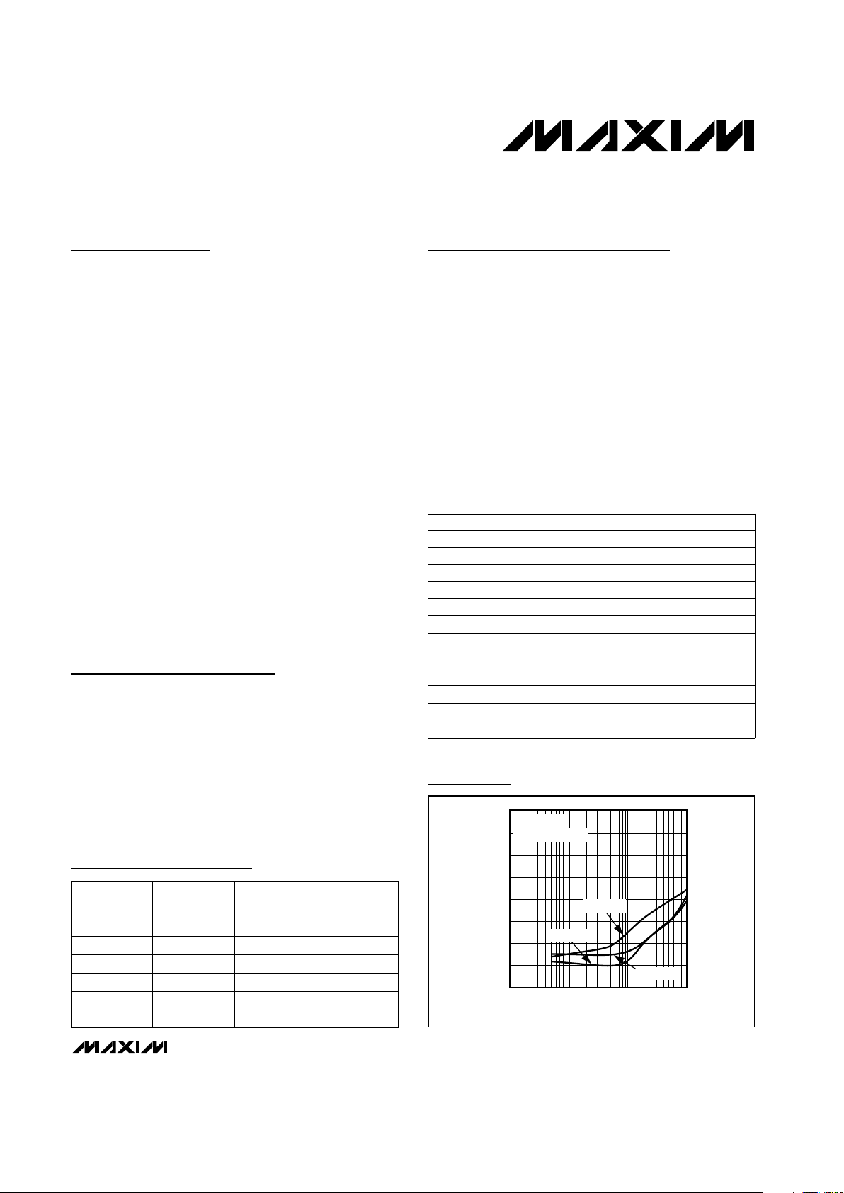
offer superior spurious-free dynamic range (SFDR) performance: -90dBc or better at frequencies below 5MHz and
-60dBc at a 100MHz frequency. Additionally, input voltage
noise density is 8nV/√Hz while operating from a single
+4.5V to +8.0V supply or from dual ±2.25V to ±4.0V supplies. These features make the MAX4265–MAX4270 ideal
for use in high-performance communications and signalprocessing applications that require low distortion and
wide bandwidth.
The MAX4265 single and MAX4268 dual unity-gain-stable
amplifiers have up to a 300MHz gain-bandwidth product.
The MAX4266 single and MAX4269 dual amplifiers have
up to a 350MHz bandwidth at a minimum stable gain of
+2V/V. The MAX4267 single and MAX4270 dual amplifiers
have a 200MHz bandwidth at a minimum stable gain of
+5V/V.
For additional power savings, these amplifiers feature a
low-power disable mode that reduces supply current to
1.6mA and places the outputs in a high-impedance state.
The MAX4265/MAX4266/MAX4267 are available in a
space-saving 8-pin µMAX package, and the MAX4268/
MAX4269/MAX4270 are available in a 16-pin QSOP package.
Applications
Base-Station Amplifiers
IF Amplifiers
High-Frequency ADC Drivers
High-Speed DAC Buffers
RF Telecom Applications
High-Frequency Signal Processing
Features
♦ +4.5V to +8.0V Single-Supply Operation
♦ Superior SFDR with 100Ω Load
-90dBc (f
C
= 5MHz )
-60dBc (f
C
= 100MHz)
♦ 35dBm IP3 (fC= 20MHz)
♦ 8nV/√Hz Voltage Noise Density
♦ 100MHz 0.1dB Gain Flatness (MAX4268)
♦ 900V/µs Slew Rate
♦ ±45mA Output Driving Capability
♦ Shutdown Mode Places Outputs in High-
Impedance State
MAX4265–MAX4270
Ultra-Low-Distortion, Single-Supply,
300MHz Op Amps with Enable
________________________________________________________________ Maxim Integrated Products 1
-20
-100
0.1M 10M 100M
-80
-90
-70
-60
-50
-40
-30
MAX4268/70 toc10
FREQUENCY (Hz)
SFDR (dBc)
1M
V
OUT
= 1Vp-p
MAX4269
MAX4270
MAX4268
RL = 100Ω to VCC/2
19-1552; Rev 0; 10/99
Selector Guide
SFDR vs. Input Frequency
Ordering Information
*Future product—contact factory for availability.
14 SO-40°C to +85°CMAX4270ESD
16 QSOP
14 SO
16 QSOP
14 SO-40°C to +85°C
-40°C to +85°C
-40°C to +85°C
-40°C to +85°C
MAX4270EEE
MAX4269ESD
MAX4269EEE
MAX4268ESD
16 QSOP
8 SO
8 µMAX
8 SO-40°C to +85°C
-40°C to +85°C
-40°C to +85°C
-40°C to +85°C
MAX4268EEE
MAX4267ESA*
MAX4267EUA*
MAX4266ESA*
8 µMAX
PIN-PACKAGETEMP. RANGE
-40°C to +85°C
MAX4266EUA*
PART
200
52MAX4270
35022MAX4269
30012MAX4268
20051MAX4267
35021MAX4266
30011MAX4265
BANDWIDTH
(MHz)
MIN GAIN
(V/V)
NO. OF
OP AMPS
PART
8 SO-40°C to +85°CMAX4265ESA*
8 µMAX-40°C to +85°C
MAX4265EUA*
Pin Configurations appear at end of data sheet.
MAX4265–MAX4270
Ultra-Low-Distortion, Single-Supply,
300MHz Op Amps with Enable
2 _______________________________________________________________________________________
ABSOLUTE MAXIMUM RATINGS
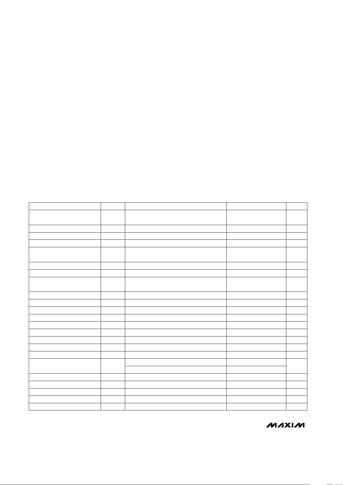
DC ELECTRICAL CHARACTERISTICS
(VCC= +5V, VEE= 0, RL= 100Ω to VCC/2, VCM= VCC/2, TA= T
MIN
to T
MAX
, typical values are at TA= +25°C, unless otherwise noted.)
Stresses beyond those listed under “Absolute Maximum Ratings” may cause permanent damage to the device. These are stress ratings only, and functional
operation of the device at these or any other conditions beyond those indicated in the operational sections of the specifications is not implied. Exposure to
absolute maximum rating conditions for extended periods may affect device reliability.
Supply Voltage (VCCto VEE)...............................................+8.5V
Voltage on Any Other Pin .................(V
EE
- 0.3V) to (VCC+ 0.3V)
Short-Circuit Duration (V
OUT
to VCCor VEE) ..............Continuous
Continuous Power Dissipation (TA= +70°C)
16-Pin QSOP (derate 8.33mW/°C above +70°C)........667mW
8-Pin µMAX (derate 4.10mW/°C above +70°C) ..........330mW
8-Pin SO (derate 5.9mW/°C above +70°C).................471mW
14-Pin SO (derate 8.33mW/°C above +70°C).............667mW
Operating Temperature Range ...........................-40°C to +85°C
Storage Temperature Range .............................-65°C to +150°C
Junction Temperature......................................................+150°C
Lead Temperature (soldering, 10s) .................................+300°C
EN_ Logic Input High Current
130
µAV
EN_
= 5V
PARAMETER SYMBOL MIN TYP MAX UNITS
Input Offset Current I
OS
0.1 5.5
µA
Input Bias Current I
B
3.5 40
µA
Input Offset Voltage Channel
Matching
1
mV
Input Offset Voltage Drift TCV
OS
1.5
µV/°C
Common-Mode Input
Resistance
R
INCM
1
MΩ
Differential Input Resistance R
INDIFF
40
kΩ
Common-Mode Rejection Ratio CMRR
60 85
dB
Power-Supply Rejection Ratio PSRR
60 85
dB
Common-Mode Input Voltage
Operating Supply Voltage
Range
V
CC
4.5 8.0
V
V
CM
VEE+ 1.6 VCC- 1.6
V
Input Offset Voltage V
OS
19
mV
Open-Loop Voltage Gain A
OL
60 95
dB
Output Current Drive I
OUT
±30 ±45
mA
Output Short-Circuit Current I
SC
100
mA
Closed-Loop Output Resistance R
OUT
0.035
Ω
Power-Up Time t
PWRUP
10
µs
Quiescent Supply Current I
S
28 32
1.6 5
Disable Output Leakage Current
0.2 5
µA
EN_ Logic Low Threshold
VCC- 3.5
V
EN_ Logic High Threshold
VCC- 1.5
V
EN_ Logic Input Low Current
5 100
µA
CONDITIONS
1.75V ≤ V
OUT
≤ 3.25V
MAX4268/MAX4269/MAX4270
Either input, (V
EE
+ 1.6) ≤ VCM≤ (VCC- 1.6)
-10mV ≤ VIN≤ 10mV
RL= 20Ω
(VEE+ 1.6V) ≤ VCM≤ (VCC- 1.6V), no load
VCC= 4.5V to 8.0V
Sinking or sourcing to VCCor V
EE
VO= 1V step, 0.1% settling time
Inferred from PSRR test
Normal mode, EN_ = 5V or floating
Inferred from CMRR test
Disable mode, EN_ = 0
V
EN_
= 0, VEE≤ V
OUT
≤ V
CC
V
EN_
= 0
Output Voltage Swing V
OUT
1.1 1.5
dBVCC- VOH, VOL- V
EE
mA
V
OUT
= 1V step
MAX4265–MAX4270
Ultra-Low-Distortion, Single-Supply,
300MHz Op Amps with Enable
_______________________________________________________________________________________ 3
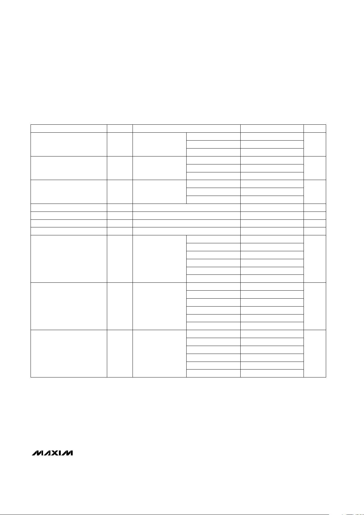
AC ELECTRICAL CHARACTERISTICS
(V
CC
= +5V, VEE= 0, RL= 100Ω to VCC/2, VCM= VCC/2, MAX4265/MAX4268 AV= +1V/V, MAX4266/MAX4269 AV= +2V/V,
MAX4267/MAX4270 A
V
= +5V/V, TA= T
MIN
to T
MAX
, unless otherwise noted. Typical values are at TA= +25°C.)
fC= 100MHz 68
fC= 60MHz 72
Third Harmonic
Distortion
dBc
fC= 20MHz 86
fC= 10MHz 92
fC= 5MHz 95
fC= 1MHz 96
V
OUT
= 1Vp-p
(MAX4269)
fC= 100MHz 60
fC= 60MHz 68
Second Harmonic
Distortion
dBc
fC= 20MHz 78
fC= 10MHz 87
fC= 5MHz 90
fC= 1MHz 88
V
OUT
= 1Vp-p
(MAX4269)
Settling Time (0.1%) tS,
0.1
15 nsV
OUT
= 1V step
Rise/Fall Times tR, t
F
1 nsV
OUT
= 1V step
Slew Rate SR 900 V/µsV
OUT
= 1V step
All-Hostile Crosstalk 85 dBf = 10MHz
MAX4267/MAX4270
MAX4266/MAX4269
MAX4265/MAX4268
0.1dB Gain Flatness BW
0.1dB
100
MHz
35
35
V
OUT
= 100mVp-p
MAX4267/MAX4270
MAX4266/MAX4269
MAX4265/MAX4268
Full-Power Bandwidth FPBW
175
MHz
200
200
V
OUT
= 1Vp-p
fC= 100MHz 60
fC= 60MHz 68
fC= 20MHz 78
fC= 10MHz 87
fC= 5MHz 90
Spurious-Free Dynamic
Range SFDR dBc
fC= 1MHz 88
V
OUT
= 1Vp-p
(MAX4269)
MAX4267/MAX4270
MAX4266/MAX4269
MAX4265/MAX4268
PARAMETER SYMBOL MIN TYP MAX UNITS
Small-Signal -3dB Bandwidth BW
-3dB
300
MHz
350
200
CONDITIONS
V
OUT
= 100mVp-p
4
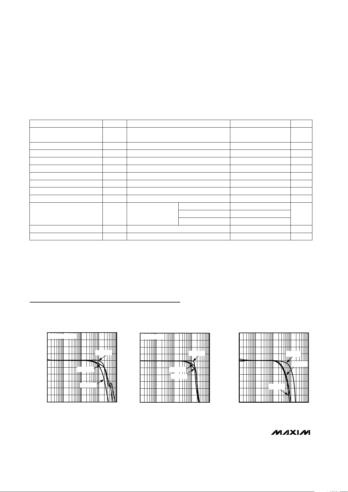
-6
0.1M 1M 10M 100M 1G
SMALL-SIGNAL BANDWIDTH
-4
MAX4268/70 toc01a
FREQUENCY (Hz)
GAIN (dB)
-2
0
2
1
-1
-3
-5
3
V
OUT
= 100mVp-p
MAX4270
MAX4269
MAX4268
Typical Operating Characteristics
(V
CC
= +5V, VEE= 0, EN_ = 5V, RL= 100Ω to VCC/2, MAX4268 AV= +1V/V, MAX4269 AV= +2V/V, MAX4270 AV= +5V/V, TA=+25°C,
unless otherwise noted.)
MAX4265–MAX4270
Ultra-Low-Distortion, Single-Supply,
300MHz Op Amps with Enable
4 _______________________________________________________________________________________
NTSC, f = 3.58MHz, RL= 150Ω to VCC/2
fC= 20MHz
V
OUT
= 1Vp-p, fCA= 20MHz,
f
CB
= 21.25MHz (MAX4269)
No sustained
oscillation
V
IN
= 1V
f = 10MHz
V
EN_
= 0
f = 1kHz
V
IN
= 1V
f = 1kHz
CONDITIONS
pA/√Hz
1i
n
Input Current Noise Density
nV/√Hz
8e
n
Input Voltage Noise Density
%0.015D
G
Differential Gain
dBm12
dBm35IP3
Two-Tone, Third-Order
Intercept Distortion
Input -1dB Compression Point
22
15
pF
15
Capacitive Load Stability
µs750t
DIS
Disable Time
pF2C
IN
Input Capacitance
Ω1R
OUT
Output Impedance
pF5Disabled Output Capacitance
ns100t
EN
Enable Time
UNITSMIN TYP MAXSYMBOLPARAMETER
MAX4265/MAX4268
MAX4266/MAX4269
MAX4267/MAX4270
NTSC, f = 3.58MHz, RL= 150Ω to VCC/2 degrees0.03D
P
Differential Phase
AC ELECTRICAL CHARACTERISTICS (continued)
(V
CC
= +5V, VEE= 0, RL= 100Ω to VCC/2, VCM= VCC/2, MAX4265/MAX4268 AV= +1V/V, MAX4266/MAX4269 AV= +2V/V,
MAX4267/MAX4270 A
V
= +5V/V, TA= T
MIN
to T
MAX
, unless otherwise noted. Typical values are at TA= +25°C.)
4
-6
0.1M 1M 10M 100M 1G
LARGE-SIGNAL GAIN
vs. FREQUENCY
-4
MAX4268/70 toc02a
FREQUENCY (Hz)
GAIN (dB)
-2
0
2
1
-1
-3
-5
3
V
OUT
= 1Vp-p
MAX4269
MAX4270
MAX4268
0.4
-0.6
0.1M 1M 10M 100M 1G
GAIN FLATNESS vs. FREQUENCY
-0.4
MAX4268/70 toc3
FREQUENCY (Hz)
GAIN (dB)
-0.2
0
0.2
0.1
-0.1
-0.3
-0.5
0.3
MAX4268
MAX4270
MAX4269
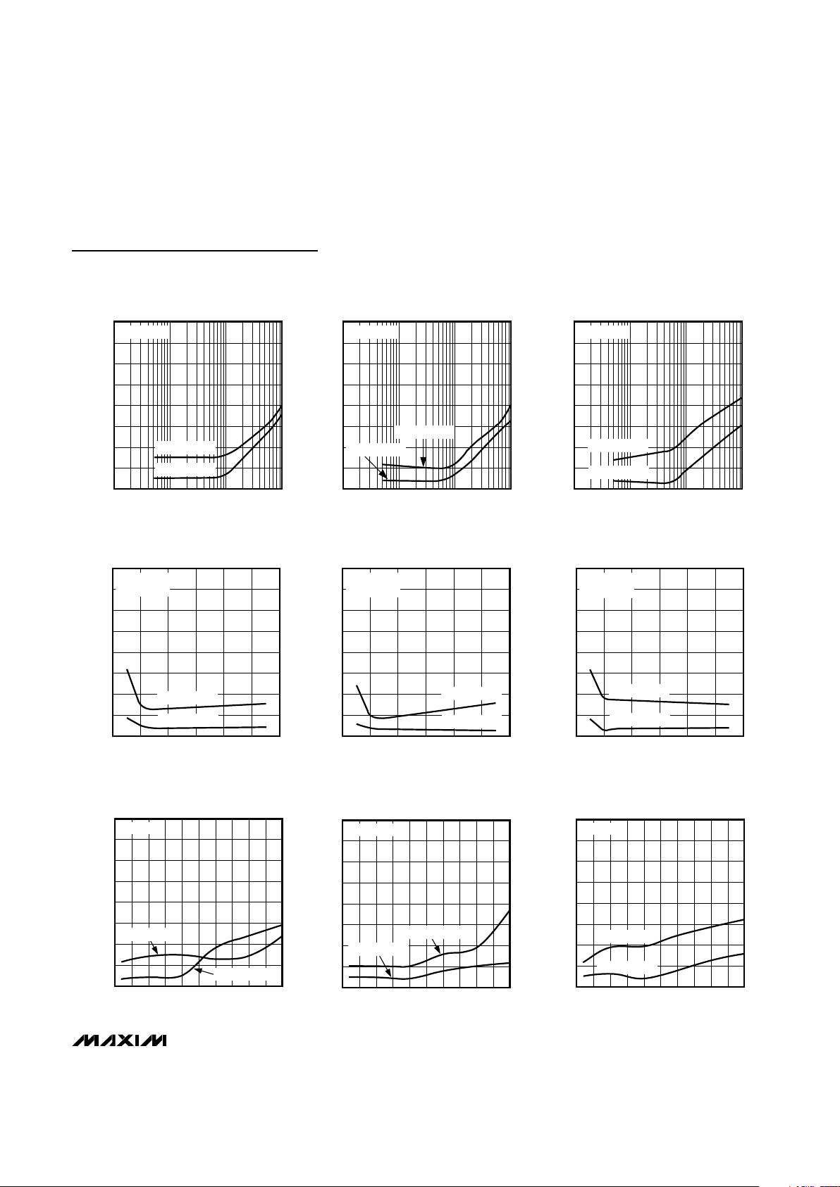
MAX4265–MAX4270
Ultra-Low-Distortion, Single-Supply,
300MHz Op Amps with Enable
_______________________________________________________________________________________ 5
Typical Operating Characteristics (continued)
(V
CC
= +5V, VEE= 0, EN_ = 5V, RL= 100Ω to VCC/2, MAX4268 AV= +1V/V, MAX4269 AV= +2V/V, MAX4270 AV= +5V/V, TA=+25°C,
unless otherwise noted.)
-20
-100
0.1M 10M 100M
MAX4268
DISTORTION vs. FREQUENCY
-80
-90
-70
-60
-50
-40
-30
MAX4268/70 toc04
FREQUENCY (Hz)
DISTORTION (dBc)
1M
2ND HARMONIC
3RD HARMONIC
V
OUT
= 1Vp-p
-20
-100
0.1M 10M 100M
MAX4269
DISTORTION vs. FREQUENCY
-80
-90
-70
-60
-50
-40
-30
MAX4268/70 toc05
FREQUENCY (Hz)
DISTORTION (dBc)
1M
V
OUT
= 1Vp-p
3RD HARMONIC
2ND HARMONIC
-20
-100
0.1M 10M 100M
MAX4270
DISTORTION vs. FREQUENCY
-80
-90
-70
-60
-50
-40
-30
MAX4268/70 toc06
FREQUENCY (Hz)
DISTORTION (dBc)
1M
V
OUT
= 1Vp-p
3RD HARMONIC
2ND HARMONIC
-100
-90
-80
-70
-60
-50
-40
-30
-20
0 200100 300 400 500 600
MAX4268
DISTORTION vs. LOAD
MAX4268/70 toc07
RESISTIVE LOAD (Ω)
DISTORTION (dBc)
fO = 5MHz
V
OUT
= 1Vp-p
3RD HARMONIC
2ND HARMONIC
-100
-90
-80
-70
-60
-50
-40
-30
-20
0 200100 300 400 500 600
MAX4269
DISTORTION vs. LOAD
MAX4268/70 toc08
RESISTIVE LOAD (Ω)
DISTORTION (dBc)
fO = 5MHz
V
OUT
= 1Vp-p
3RD HARMONIC
2ND HARMONIC
-100
-90
-80
-70
-60
-50
-40
-30
-20
0 200100 300 400 500 600
MAX4270
DISTORTION vs. LOAD
MAX4268/70 toc09
RESISTIVE LOAD (Ω)
DISTORTION (dBc)
fO = 5MHz
V
OUT
= 1Vp-p
3RD HARMONIC
2ND HARMONIC
-100
-80
-90
-70
-40
-30
-50
-60
-20
0 0.5 1.0 1.5 2.0 2.5
MAX4268
DISTORTION vs. VOLTAGE SWING
MAX4268/70 toc10
VOLTAGE SWING (Vp-p)
DISTORTION (dBc)
fO = 5MHz
3RD HARMONIC
2ND HARMONIC
-100
-80
-90
-70
-40
-30
-50
-60
-20
0 0.5 1.0 1.5 2.0 2.5
MAX4269
DISTORTION vs. VOLTAGE SWING
MAX4268/70 toc11
VOLTAGE SWING (Vp-p)
DISTORTION (dBc)
fO = 5MHz
3RD HARMONIC
2ND HARMONIC
-100
-80
-90
-70
-40
-30
-50
-60
-20
0 0.5 1.0 1.5 2.0 2.5
MAX4270
DISTORTION vs. VOLTAGE SWING
MAX4268/70 toc12
VOLTAGE SWING (Vp-p)
DISTORTION (dBc)
fO = 5MHz
3RD HARMONIC
2ND HARMONIC
 Loading...